
11
Molecular Beam Epitaxial Growth of Terahertz Quantum Cascade Lasers
Harvey E. Beere and David A. Ritchie
Department of Physics, Cavendish Laboratory, University of Cambridge, Cambridge, CB3 0HE, UK
11.1 Introduction
The terahertz (THz) frequency region of the electromagnetic spectrum (1–10 THz; ∼300–30 µm; 4–40 meV) has many important potential applications such as imaging, chemical spectroscopy and telecommunications [1]. This is a combination of the unique properties associated with this frequency regime. The penetration depth of THz waves through many materials in ordinary use, such as plastic and cloth, increases substantially with decreasing frequency. The vibrational modes of large molecules are in this frequency range, lending it to both chemical and biomedical sensing and imaging. In space, most molecules emit their rotational spectra in the THz, allowing processes in star formation and interstellar medium (gas clouds) to be observed. Communications over this frequency band are currently unallocated and have the potential for fast, terabit‐per‐second data link capacities.
Consequently, there has been a strong drive to develop compact, low‐cost, efficient THz sources. Although semiconductor devices traditionally account for a large share of the sources of electromagnetic waves, the THz range has remained substantially uncovered. The demonstration of the THz quantum cascade laser (QCL) in 2002 provided a potential solid‐state solution [2]. Significant progress has been made in subsequent years, offering frequencies from 1.2 to 5 THz [3], maximum operating temperatures approaching 200 K [4], peak output powers >2 W [5] and an ultra‐broadband (>1 THz) operating frequency range from a single laser [6].
Any THz QCL needs to surmount two fundamental problems. The first is how to achieve large carrier population inversions below the longitudinal optical (LO) phonon energy (34–36 meV; 8–9 THz), since direct electron‐LO phonon scattering processes are traditionally used in mid‐infrared QCL designs [7]. The second challenge is to develop a suitable waveguide with low free‐carrier absorption losses that can confine the long‐wavelength light to an epilayer that is compatible with epitaxial growth techniques.
QCLs are unipolar devices that are based on inter‐subband transitions of electrons in the conduction band of a specifically engineered semiconductor heterostructure. This is in contrast to a conventional solid‐state semiconductor laser that relies on the radiative recombination of conduction band electrons with valence band holes across the band gap of the active semiconductor material. Since the energy and envelope functions of the subbands in a QCL structure can be controlled by the thickness of the individual layers and by the applied bias, the band gap of the semiconductor is, for the most part, irrelevant. Consequently, mature material systems such as GaAs/AlGaAs [ 4– 6], InGaAs/InAlAs [8] and InGaAs/GaAsSb [9] have been utilised to produce THz QCLs.
To this end, an active ‘gain’ region typically hosts three levels, of which the upper two (levels 1 and 2) form the laser transition, and the third efficiently extracts electrons from the lower laser state to maintain population inversion. These active regions are connected by injector/extraction structures that collect electrons from the previous active region, cool down the carrier distribution and inject them again into the upper laser level of the following active region. Injector/collector regions and active regions constitute a building block (so‐called ‘period’) that can be repeated many times, typically 100–200. Under appropriate bias, all periods line up to form the potential ‘cascade’, the active core of the laser, in which the electrons travel downstream, emitting ideally one photon at each step of the cascade.
Figure 11.1 shows the conduction band profiles for two different THz QCL active region designs under optimal lasing bias. Figure 11.1(a) shows a bound‐to‐continuum design comprising 18 individual layers, nine GaAs quantum wells and nine Al0.15Ga0.85As barriers, which in a full laser design will be repeated 90 times [10]. The lasing transition was designed to be 11 meV or 2.66 THz under an applied electric field of 2.1 kV cm−1. Figure 11.1(b) shows a short bound‐to‐continuum design with a single quantum well phonon extraction/injection stage comprising eight individual layers, four GaAs quantum wells and four Al0.15Ga0.85As barriers, which in a full laser design will be repeated 160–180 times [12]. The lasing transition was designed to be 12 meV or 2.90 THz under an applied electric field of 7.6 kV cm−1. Doping in the injection structures for both designs is required to ensure, during operation, that there are enough carriers to avoid depletion and space‐charge formation, whilst keeping free carrier absorption to a minimum.
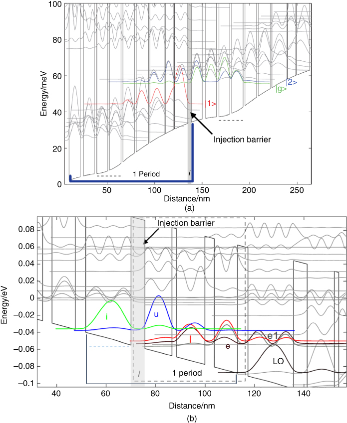
Figure 11.1 Self‐consistent calculation of portions of the conduction band diagram under optimal lasing bias for (a) 2.7 THz bound‐to‐continuum design with miniband extraction [10] under applied electric field of 2.1 kV cm−1 (Source: Reproduced from [11]) and (b) 3 THz bound‐to‐continuum with a phonon extraction/injection design [12] under applied electric field of 7.6 kV cm−1 (Source: Reproduced from [13]). Labelled states are upper laser (|2> or u), lower laser (|1> or l) and injector (|g> or i), respectively.
Another significant challenge in the production of a solid‐state THz laser was the development of a suitable waveguide to confine the long‐wavelength light to an epilayer compatible with epitaxial technologies without imposing high absorption losses onto the laser mode. Two classic waveguiding approaches have been adopted, the single plasmon waveguide [2] and the metal–metal waveguide [14]. However, the recent development of the hybrid plasmonic waveguide offers an interesting approach that combines the advantages of both waveguide designs [15]. For further reading in the differences in active region design and the classes of THz QCL waveguide, excellent reviews are given in Refs [16,17]. The complete THz QCL structure comprises many repeats of this active region, typically 10 µm thick, embedded between top and bottom heavily doped layers, that not only facilitate waveguiding but also provide electrical contacts. The epitaxial wafer is then processed into a laser device using conventional semiconductor processing, and mounted onto the cold head of a cryostat, as described in Ref. [18]. Consequently, the epitaxial growth for any THz QCL, irrespective of active region design, comprises 1200–1600 individual layers.
Figure 11.2(a) shows the current versus voltage (I–V) and current–light (I–L) characteristics of a bound‐to‐continuum QCL design shown in Figure 11.1(a), driven in pulsed mode. In order to avoid atmospheric‐water absorption, the emitted light was collected with the whole optical path under a vacuum. The threshold current density, Jth, at 4 K is 104 A cm−2, achieving a peak power of 77 mW (assuming an estimated collection efficiency of 30%, as described in Ref. [10]) at 207 A cm−2 (Jmax). Raising the device temperature results in an increase of the threshold current density, up to 225 A cm−2 at the maximum operating temperature of this device. This can be interpreted as activated LO‐phonon depopulation of the upper state. Emission spectra are shown in Figure 11.2(b) for different drive currents measured at 4 K using a Fourier transform infrared spectrometer (7.5 GHz resolution). Up to 1.2 A (160 A cm−2), the laser emits in a single frequency mode at 2.66 THz (10.99 meV), which is in excellent agreement with the design. Pronounced multimode frequency emission is then observed for higher drive currents, in the range 2.61–2.72 THz, showing equally spaced longitudinal Fabry–Pérot cavity modes with a spacing of 12.75 GHz. The missing mode at 2.68 THz is due to an atmospheric H2O absorption line.
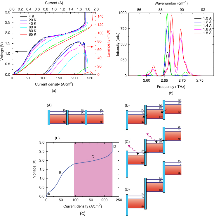
Figure 11.2 (a) Voltage and emitted light power as a function of current density at different heat sink temperatures, for a 3 mm long, 250 µm wide laser ridge, for the 2.7 THz bound‐to‐continuum QCL design with single plasmon waveguide [10]. The laser was driven in pulsed mode, with a 20 kHz repetition rate and a 0.5% duty cycle. (b) Frequency spectra measured at 4 K for different laser currents. (c) Schematic diagram of QCL operation at different biases. Laser emission occurs in region (C)
(Source: Reproduced from [19]).
Figure 11.2(c) illustrates in a simplified form the stages of laser operation with respect to the alignment of the active region band diagram. The upper laser state, lower laser state and injector ground state are indicated by |2>, |1>, and |g>, respectively. The lower extraction/injection miniband for the bound‐to‐continuum design is illustrated by the horizontal red band, the injection barrier by the vertical blue bar. There are four regions marked on the I–V diagram: (A), (B), (C) and (D). Region (A) corresponds to zero bias, where there is no current flowing. Region (B) corresponds to the device under low applied bias and the structure has yet to become aligned. Lasing cannot take place, but a small leakage path between the extraction/injection states to the next period is present (arrows). Region (C) shows the active region periods under alignment bias, when the laser gain overcomes device loss at current threshold Jth. It is in this aligned bias regime that lasing can occur, when the active region is incorporated into an appropriately designed waveguide. Eventually the structure misaligns, region (D), where states |g> and |2> anti‐cross, which is the region where laser action ceases as current flow through the structure breaks down. This is observed as a rapid decrease in the differential resistance of the device, and is mainly due to the loss of photo‐induced current. The photo‐assisted current is highly visible at the threshold as a discontinuous drop in the differential resistance. The magnitude of this discontinuity has been associated with the ratio of upper state to lower state lifetime [20] and is an indication of active region performance.
11.2 Epitaxial Challenges
The growth of THz QCLs is extremely challenging, owing to the stringent demands for precise control of individual layer thicknesses and alloy compositions, which must be maintained over the entire active region, typically 10 µm. Using typical molecular beam epitaxy (MBE) growth rates for the GaAs/AlGaAs material system, namely 1.00 µm h−1 for GaAs and 0.10–0.25 µm h−1 for AlAs (∼10–20% aluminium barrier composition), the growth time for any laser is in excess of 12 hours. This places tight tolerances on the accuracy, stability and uniformity of the MBE growth.
11.2.1 Growth Rate Calibration
The operation of a THz QCL is strongly dependent on the repeatable production of the correct thicknesses of wells and barriers throughout the growth of the active region stack. Figure 11.3 shows the theoretical emission frequency (photon transition energy) as a function of global active region thickness for two different active region designs, a 2.7 THz bound‐to‐continuum design [10] and a 3 THz bound‐to‐continuum with phonon extraction/injection design [12]. Each simulation point (open circles) represents a self‐consistent calculation for commensurate percentage changes in global well and barrier thickness for the two designs. The alignment condition was taken as the field at which anti‐crossing between the upper and injector states occurs, as this resonance characterises a maximum in device conduction. Both designs show that the thickness of each active region should be within ±1% of the design to achieve emission within ±0.05 THz (approx. ±0.25 meV). As the composition of most THz QCL designs comprises >95% GaAs, this is the dominant growth rate to calibrate and monitor. Analysis of the first THz QCL design [18] indicated that the growth rate calibration of the barrier composition alloy, AlAs, affects the optical transition energy less, with a 5–10% calibration window. For barrier layers containing low percentage alloy compositions this is not surprising, however, due to the tunnelling transport nature of the carrier injector scheme in this type of device, this value will be tighter to achieve optimal laser performance [21].

Figure 11.3 Emission frequency against measured active region period thickness for QCL wafers growths on a Veeco modGENII MBE system for (a) 2.7 THz bound‐to‐continuum design [10] and (b) 3.0 THz bound‐to‐continuum with phonon extraction/injection design [12]. The connected (blue) points are the predicted emission frequencies from self‐consistent band structure calculations.
Looking in closer detail at the simulated theoretical variation in design lasing frequency as a function of active region period thickness for the two designs, there are a number of similarities but also differences. Firstly, there is a trend, with active regions thicker than the nominal design to red shift. However, for active regions thinner than the nominal design, the bound‐to‐continuum blue shifts whereas the bound‐to‐continuum with phonon extraction appears to plateau. For the bound‐to‐continuum design there is an approximate linear variation over a 10% change of active region thickness, such that the frequency of the design can be tuned over ∼440 GHz, shifting by ∼44 GHz per percentage change in layer thickness. For the bound‐to‐continuum with phonon extraction design, this linear blue shift is only observed when increasing the layers above their nominal design, again producing ∼40 GHz per percentage change in active region thickness.
Also plotted in Figure 11.3 are twelve and six QCL wafer growths of the two active region designs, respectively (black squares), performed on a Veeco modGenII MBE chamber that includes a set of deliberate variations in global thickness to verify the simulations. The period length of each QCL wafer was determined by high‐resolution X‐ray diffraction, fitting the spacing of the satellite peaks around the [004] lattice reflection with an accuracy of 0.5% [22]. Each wafer was processed into 250 µm wide by 3 mm long ridges using a single plasmon waveguide architecture from the centre location of the grown wafer. The frequency plotted for each wafer is the centre frequency at maximum laser power, measured using a Fourier transform infrared spectrometer with 7.5 GHz resolution. This is when the structure is fully aligned and maximum current is being passed (Jmax). Clearly, there is very good agreement between the data from the wafers and the simulations for both the THz QCL designs [23]. A similar tuning trend has also been observed in Ref. [24] for the 2.7 THz bound‐to‐continuum design, demonstrating a 160 GHz reduction in frequency for a +4% increase in Ga growth rate. A similar 110 GHz decrease in frequency shift was observed for a 3% thickness increase for a 2.0 THz bound‐to‐continuum active region design, showing the robustness of this active region design [25].
We have seen the effect systematic scaling of the active region has on the emission frequency of a 2.7 THz bound‐to‐continuum design. This leads us to question what effect this engineering will have on the electrical properties of the laser. Simulations of the electrical properties were modelled [11], suggesting that a thicker structure should have lower alignment fields and a smaller splitting between the injector and upper states. The reduction in both alignment field and magnitude of the anti‐crossing with increased thickness should be observed as a decrease in bias at Jmax. The anti‐crossing between the injector and the upper state is related to Jmax, because the bottleneck for electron transport is the thickest barrier, known as the injection barrier.
Figure 11.4 shows the experimental results for a series of QCL device growths to test this prediction. A reference wafer (V433) was grown to the published design [10], except that there were only 45 repeats of the active region. Two further wafers were grown with all the wells and barriers 5% thinner (V431) and 5% thicker (V434); the wafer designs were the same as the reference in all other respects. From the electrical data in Figure 11.4(a) we can see that the experimental results are in good agreement with the predictions from the simulations. The thicker structure (V434) reaches maximum power at a lower field and has a lower current at maximum power. We see that the opposite is true for the thinner structure (V431), which has a higher Jmax and higher bias at maximum power than the reference (V433). The period lengths for the wafers were obtained by X‐ray diffraction, with this trend being clearly shown in Figure 11.4(c). The frequencies of each design also agree with the simulation data presented in Figure 11.3(a), showing that these devices cover an ∼300 GHz range. Clearly the performance of the laser structures has been affected dramatically by varying the global thicknesses of the layers, suggesting that optimal laser performance is achieved only around the nominal design, reinforcing the stringent growth accuracy required for each layer thickness.
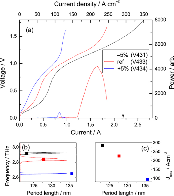
Figure 11.4 (a) Voltage and emitted light power as a function of current density at 4 K for three QCL wafers based on the 2.7 THz bound‐to‐continuum design [10], intentionally grown nominally 5% thinner (V431) than the original design (V433) and nominally 5% thicker (V434). All devices are single plasmon waveguides, 3 mm × 250 µm. The lasers were driven in pulsed mode, with a 10 kHz repetition rate and a 1% duty cycle. The device from V432 lased weakly and the maximum power is indicated by the arrow. (b) Frequency as a function of measured period length and pulsed spectra from the devices. (c) The current at maximum laser power, Jmax, as a function of period length.
(Source: Reproduced from [11]).
However, this global approach has some merit as a starting methodology to modify a known QCL design in a simple and predictable way to tailor the frequency emission. A similar experimental study was undertaken in Ref. [11] by investigating the effect of globally scaling only the well thicknesses. Scaling by ±5% the wells of the 2.7 THz bound‐to‐continuum design resulted in a commensurate frequency tuning response; a longer structure having larger wells having a lower frequency, achieving again a frequency span of ∼400 GHz. This should not be surprising considering that the majority of the active region thickness in a bound‐to‐continuum design is made up of wells. The effect on transport was as predicted, but not as extreme. Whilst the trend in Jmax was consistent, the absolute difference between the three wafers in Figure 11.4(a) was significantly reduced. Again, this should not be too surprising as the absolute barrier thickness of these devices has not changed and one naively expects that the barriers will have more effect on the transport characteristics. The thinner structure still showed very poor lasing performance, however the thicker structure outperformed the original design in both higher light output power, maximum temperature of operation and a lower threshold current.
This methodology was used to produce a series of THz QCL designs between 2.6 and 3.0 THz, operating with the same alignment electric field and matched maximum operating current (i.e. maximum light output); this was done by scaling the wells of the QCL design in Ref. [10] to achieve the desired emission frequency and then modifying the thickness of the barrier layers to harmonise the maximum operating current [11]. Two matched designs were then incorporated into a single broad gain heterogeneous structure [26]. The dual stack heterogeneous QCL wafer demonstrated in a single plasmon waveguide simultaneously two frequency emissions at 2.6 and 2.9 THz and in a metal–metal waveguide continuous lasing over a ∼400 GHz bandwidth [27]. An alternative heterogeneous scheme incorporated 23 laser stacks of the 2.7 THz bound‐to‐continuum QCL that stepwise reduced the Ga growth rate from +6 to −4% of the nominal growth rate for the design. This produced electrically tunable frequency emission over a 330 GHz bandwidth [28].
A similar approach modifying the thickness of the optical transition wells in the short bound‐to‐continuum design with a single quantum well phonon extraction/injection stage [12] achieved QCLs spanning 2.3–3.1 THz, although they operated with different alignment fields and operating current ranges [29]. Three active regions were incorporated into a five‐stack heterogeneous design using a metal–metal waveguide, producing the >1 THz continuous emission from a single device [ 6,30] that is the basis for THz frequency comb lasers [31].
Conventionally, MBE material deposition rates are calibrated in one of two ways, either (i) by ex‐situ measurements of the thickness of calibration layers or (ii) by using in‐situ reflection high‐energy electron diffraction (RHEED) oscillations. To calibrate for the extremely long growth durations needed for THz QCL growth (>12 hours), RHEED is not appropriate as it, (a) cannot measure beyond a few tens of nanometers of layer growth, which can include any initial cell flux transients, and (b) is usually restricted to non‐rotating substrates, so that it may not reflect the true steady‐state growth rates. For THz QCL growth, two calibration approaches have been reported. The first uses the ex‐situ X‐ray diffraction of a simple periodic calibration structure. The respective binary epitaxial layers of the QCL structure are incorporated into a short superlattice (e.g. GaAs/AlAs), which can determine the thicknesses of the individual layers, and hence the respective growth rates. This approach has been used successfully to calibrate both the GaAs/AlGaAs and InGaAs/InAlAs material systems before THz QCL growth [32]. The second calibration approach uses an in‐situ optical measurement, which is desirable as it is a real‐time measurement that is relatively insensitive to any rotation, vibration, wobbling or misalignment of the wafer. Optical thickness measurements [33,34] using a single colour pyrometer (0.94 µm) were used to grow the first THz QCLs and were shown to have a measurement accuracy better than 1% [18]. This has been extended over a wider range of frequencies using pyrometric spectroscopy, which not only facilitates the pre‐growth optical growth rate calibrations, but also allows in‐situ monitoring during the QCL growth [35]. Both growth rate calibration techniques have demonstrated the ±1% accuracy in growth rate needed to ensure optimal growth of the intended design.
11.2.2 Growth Rate Stability
Owing to the extremely long growth durations associated with THz QCL growth, another potential error associated with the epitaxy is any drift from the matrix elements effusion cells (i.e. material depletion and movement). In Section 11.2.1 it was shown that an epitaxial window of ±1% is required to achieve accurate growth of most laser designs. Table 11.1 shows the measured GaAs and AlAs growth rates using single colour optical pyrometry, taken directly before and then after several standard THz QCL growths (∼12–13 µm total thickness), corresponding to an approximate 15‐hour time interval between measurements, for a number of different effusion cells on two different manufacturer's MBE systems. The data is representative of numerous measurements taken from these cells over multiple growth campaigns using a minimum of three optical thickness oscillations for the GaAs and two oscillations for the AlAs calibration layers.
Table 11.1 GaAs and AlAs growth rates measured by optical pyrometry directly before and after two ∼15‐hour QCL sample growths undertaken on a VG Semicon V80H MBE system and a Veeco modGENII MBE system for a number of different effusion cell designs. Estimated measurement accuracy is <1% [18]
| Before (µm h−1) | After (µm h−1) | Drift (%) | Before (µm h−1) | After (µm h−1) | Drift (%) |
| VG Semicon V80H Ga | EPI‐Veeco 85cc dual filament cell | VG Semicon V80H Al | VG 40cc conical single filament cell | ||
| 0.9946 | 0.9872 | −0.74 | 0.1764 | 0.1749 | −0.85 |
| 0.9969 | 0.9924 | −0.45 | 0.1765 | 0.1754 | −0.62 |
| Veeco modGENII Ga | Veeco 400 g SUMO dual filament cell | Veeco modGENII Al | Veeco 400 g SUMO dual filament cell | ||
| 1.004 | 1.009 | +0.50 | 0.1786 | 0.1770 | −0.90 |
| 1.008 | 0.995 | −1.29 | 0.1782 | 0.1778 | −0.22 |
| Veeco modGENII Ga | Veeco 250 g DWL SUMO dual filament cell | ||||
| 1.0062 | 1.0023 | −0.40 | |||
| 1.0028 | 0.9991 | −0.40 |
For the five effusion cells used, all the measured growth rate drifts for a standard THz QCL design growth thickness are generally within the 1% margin of accuracy desired. All the effusion cells are standard, commercially available designs for their respective MBE growth systems. The EPI‐Veeco 85 cc dual filament cell includes a low flux transient insert pointing at the centre of the wafer. It is interesting to note that although most measurements show that material depletion dominates (i.e. a negative drift), at the beginning of a growth campaign, material movement for both a fully filled Ga and Al cell can give a positive flux drift. Furthermore, at the end of a growth campaign, cell depletion during growth of a QCL can give rise to downward drifts nearer 2%, especially for the Al cells, which will affect laser performance. For longer growth durations, necessary for thicker active region designs associated with high power lasers or for cells with higher material depletion profiles, an appropriate predetermined temperature ramp can be introduced to compensate for this [35].
11.2.3 Growth Rate Uniformity
Although temporal stability of the matrix element fluxes is a key requirement for the growth of THz QCLs, uniformity of deposition across a growing wafer is equally important. Table 11.2 shows the measured radial uniformity of GaAs and AlAs growth rates using an ex‐situ X‐ray diffraction measurement of a two‐period superlattice structure [36,37], for five different effusion cells on two different manufacturer's MBE systems. The data is representative of numerous measurements taken from these cells over multiple growth campaigns.
Table 11.2 GaAs and AlAs growth rates uniformity measured by high‐resolution X‐ray diffraction from different effusion cells performed on a VG80H MBE system and a Veeco modGENII MBE system. Estimated measurement accuracy for growth rates is <1% [37]
| VG Semicon V80H Ga | EPI‐Veeco 85cc dual filament cell | VG Semicon V80H Al | VG 40cc conical single filament cell | ||
| 1″ Variation | 2″ Variation | 1″ Variation | 2″ Variation | ||
| −0.31% | −1.29% | +0.21% | −2.54% | ||
| Veeco modGENIIGa | Veeco 400 g SUMO dual filament cell | Veeco modGENII Al | Veeco 400 g SUMO dual filament cell | ||
| 1″ Variation | 2″ Variation | 3″ Variation | 1″ Variation | 2″ Variation | 3″ Variation |
| +0.06% | −1.09% | −2.46% | −0.28% | −1.07% | −2.60% |
| Veeco | Veeco 250 g DWL SUMO | ||||
| modGENII | dual filament cell | ||||
| Ga | |||||
| 1″ Variation | 2″ Variation | 3″ Variation | |||
| +0.04% | +0.02% | −1.27% | |||
For the five effusion cells measured, the radial growth rates show a large variation. For all the Ga cell designs an ∼1% variation is observed within a 2‐inch radius. For the modGENII MBE system, the 400 g SUMO® had a greater variation than the 250 g downward looking (DWL) SUMO®. This is confirmed by the 125 GHz frequency shift in the 2.7 THz bound‐to‐continuum design observed from THz QCL devices processed from the centre of the wafer and the edge grown by the 400 g SUMO Ga cell [23]. Although the VG Semicon VG80H is nominally a 3‐inch growth platform, the above data for the cells used showed that to achieve the required few percent variation window, only 2‐inch substrates could be used for epitaxy of QCLs on this particular system. A greater radial variation was observed for the Al cells, however this is unsurprising due to the tendency of molten Al to wet the pyrolytic boron nitride (PBN) crucible, resulting in a fluctuating, unstable melt front. However, for the current class of GaAs/AlGaAs THz QCLs designs, the flux window for Al is relaxed owing to the low ternary composition in the barriers.
The uniformity of deposition from any effusion cell is dependent not only on the geometry of the MBE system [38], the cell and crucible design [39], but also the evaporation ‘melt’ front of the source material. Consequently, deposition uniformity can vary over the course of an MBE growth campaign, as material depletion alters the area of this evaporating melt front [40]. Using crucible inserts not only reduces flux transients, due to the increased radiation shielding, but allows a constant melt area as seen from the substrate position, even as the melt location recedes [41]. In Ref. [42] the authors show the difference in deposition uniformity when using different effusion sources on a production VG Semicon V90 MBE system. Across a 3‐inch substrate a Ga cell using graphite inserts gave a uniformity <0.2%, whereas a Ga SUMO cell gave <1% variation. In comparison, for Al, a <0.5% variation was seen for a 30 cc conical crucible but this increased to ∼11% for an Al SUMO cell design. However, the SUMO uniformity could be improved by optimising the initial cell fill and the temperature gradient between the cold lip zone and the melt (body), to minimise material creep.
11.2.4 Doping Accuracy
For the epitaxy of III–V semiconductors and particularly the MBE growth of the GaAs and InGaAs material systems, the most common dopants are silicon (n‐type), tin (n), carbon (p‐type) and beryllium (p). Determination of the doping level can be achieved by a variety of methods, however all generally use a set of thick homogeneously doped (volumic doping) epitaxially grown calibration layers. The individual layers are doped in the range spanning 1 × 10¹⁵–5 × 1018 cm−3, with the dopant density measured by either capacitance–voltage (CV) profilometry, secondary ion mass spectrometry (SIMS) or Hall measurements [43]. By far the most reported calibration method for THz QCL growth is ex‐situ Hall measurements [ 18, 32, 35]. At the start of a typical growth campaign, a minimum of six to eight samples are grown to produce a doping calibration curve. Throughout the chamber's growth campaign, additional bulk doped samples are periodically repeated to check the calibration curve's integrity; this is critical for the injection doping levels in the 1016 cm−3 regimes.
Figure 11.5 shows the key laser operating parameters, threshold current density (Jth), maximum current density (Jmax) and maximum temperature of operation (Tmax) as a function of sheet doping concentration in the active region injector for three different classes of THz QCL design. All designs show similar characteristics; the threshold and maximum lasing currents increase linearly with active region doping and there appears an optimal doping to achieve maximum temperature of operation. These characteristics have also been observed in a 3.45 THz bound‐to‐continuum [45] and a 2.75 THz LO phonon extraction design [46]. Increasing the doping level in the injector has been exploited to produce the highest reported THz output powers [5].
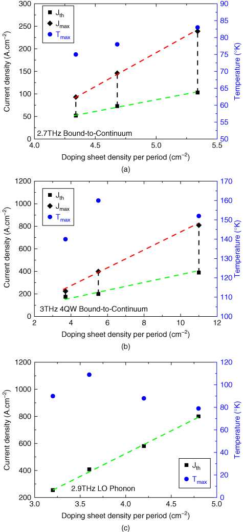
Figure 11.5 Measured laser operating performance, Jth and Jmax, at 10 K and maximum operating temperature, Tmax, as a function of normalised sheet doping concentration, for (a) 2.7 THz bound‐to‐continuum design [ 10, 21], (b) 3 THz bound‐to‐continuum with phonon extraction/injection design and (c) 2.9 THz LO phonon extraction design
(Source: Data from [44]).
(Source: Data from [12])
Reference [45] shows that the key influence on this linear increase originates from the increase in losses due to free carrier absorption in the active region. However, Ref. [46] shows that this is not the case for extremely low doped active regions and that waveguide losses become important. Interestingly, the linear relationship between doping and the lasing threshold in all these QCLs designs for any doping level shows that the background impurity level in the MBE system is not yet a limiting factor.
References
- 1 Tonouchi, M. (2007). Nat. Photonics 1 (2): 97.
- 2 Köhler, R., Tredicucci, A., Beltram, F. et al. (2002). Nature 417: 157.
- 3 Kumar, S. (2011). IEEE J. Select. Top. Quantum Electron. 17 (1): 38.
- 4 Fathololoumi, S., Dupont, E., Chan, C.W.I. et al. (2012). Opt. Express 20 (4): 3866.
- 5 Li, L.H., Chen, L., Freeman, J.R. et al. (2017). Electron. Lett 53 (12): 799.
- 6 Rösch, M., Scalari, G., Beck, M., and Faist, J. (2014). Nat. Photonics 9 (1): 42.
- 7 Faist, J., Capasso, F., Sivco, D.L. et al. (1994). Science 264: 553.
- 8 Fischer, M., Scalari, G., Celebi, K. et al. (2010). Appl. Phys. Lett. 97 (22): 221114.
- 9 Deutsch, C., Krall, M., Brandstetter, M. et al. (2012). J. Appl. Phys. Lett. 101 (21): 211117.
- 10 Barbieri, S., Alton, J., Beere, H.E. et al. (2004). Appl. Phys. Lett. 85 (10): 1674.
- 11 J. R. Freeman, PhD thesis ‘Heterogeneous terahertz quantum cascade lasers’, University of Cambridge (2009).
- 12 Amanti, M.I., Scalari, G., Terazzi, R. et al. (2009). New J. Phys. 11: 125022.
- 13 Y. D. Shah, PhD thesis ‘Novel designs and waveguides in terahertz quantum cascade lasers’, University of Cambridge (2017).
- 14 Williams, B.S., Kumar, S., Hu, Q., and Reno, J.L. (2005). Opt. Express 13 (9): 3331.
- 15 Degl'Innocenti, R., Shah, Y.D., Wallis, R. et al. (2015). Appl. Phys. Lett. 106: 082101.
- 16 Williams, B.S. (2007). Nat. Photonics 5: 17.
- 17 Faist, J. (2013). Quantum Cascade Lasers. Oxford: Oxford University Press.
- 18 Beere, H.E., Fowler, J.C., Alton, J. et al. (2005). J. Cryst. Growth 278: 756.
- 19 O. P. Marshall, PhD thesis ‘Terahertz quantum cascade lasers: Photonic crystal waveguides and high frequency bias modulations’, University of Cambridge (2009).
- 20 Sirtori, C., Capasso, F., Faist, J. et al. (1998). IEEE J. Quantum Electron. 34 (9): 1722.
- 21 Alton, J., Barbieri, S., Worrall, C. et al. (2005). Terahertz and Gigahertz Electronics and Photonics IV, SPIE Proceedings, vol. 5727. New York: SPIE.
- 22 Bowden, K. and Tanner, B.K. (1998). High Resolution X‐Ray Diffractometry and Topography. New York: Taylor & Francis.
- 23 Freeman, J.R., Worrall, C., Apostolopoulos, V. et al. (2008). IEEE Photonics Technol. Lett. 20 (4): 303.
- 24 Khannaa, S.P., Chakraborty, S., Lachab, M. et al. (2008). Physica E 40: 1859.
- 25 Beere, H.E., Worrall, C.H., Whelan, S. et al. (2007). J. Cryst. Growth 301&302: 935.
- 26 Gmachl, C., Sivco, L., Colombelli, R. et al. (2002). Nature 415: 883.
- 27 Freeman, J.R., Brewer, A., Madéo, J. et al. (2011). Appl. Phys. Lett. 99: 241108.
- 28 Khanna, S.P., Salih, M., Dean, P. et al. (2009). Appl. Phys. Lett. 95: 181101.
- 29 Turčinkova, D., Scalari, G., Amanti, M.I. et al. (2011). Novel In‐Plane Semiconductor Lasers X, SPIE Proceedings, vol. 7953. New York: SPIE.
- 30 Turčinkova, D., Scalari, G., Castellano, F. et al. (2011). Appl. Phys. Lett. 99 (19): 191104.
- 31 Faist, J., Villares, G., Scalari, G. et al. (2016). Nanophotonics 5 (2): 272.
- 32 M. Fischer, PhD thesis ‘Terahertz quantum cascade lasers based on InGaAs/InAlAs/InP semiconductors’, ETH Zürich (2011).
- 33 SpringThorpe, A.J., Humphreys, T.P., Majeed, A., and Moore, W.T. (1989). Appl. Phys. Lett. 55 (20): 2138.
- 34 Boebel, F.G., Möller, H., Hertel, B. et al. (1995). J. Cryst. Growth 150: 54.
- 35 Li, L.H., Zhu, J.X., Chen, L. et al. (2015). Opt. Express 23 (3): 2720.
- 36 J. Fowler, PhD thesis ‘A study of the performance of terahertz quantum cascade devices’, University of Cambridge (2005).
- 37 P. J. Simmonds, PhD thesis ‘Molecular beam epitaxy of InGaAs and InAlAs for low‐dimensional electrical transport’, University of Cambridge (2007).
- 38 Shiralagi, K.T., Kriman, A.M., and Maracas, G.N. (1991). J. Vac. Sci. Technol., A 9 (1): 65.
- 39 Aers, G.C. and Wasilewski, Z.R. (1992). J. Vac. Sci. Technol., B 10 (2): 815.
- 40 Herman, M.A. and Sitter, H. (1996). Molecular Beam Epitaxy: Fundamentals and Current Status. New York: Springer‐Verlag.
- 41 Maki, P.A., Palmateer, S.C., Calawa, A.R., and Lee, B.R. (1986). J. Vac. Sci. Technol., B 4 (2): 564.
- 42 Wasilewski, Z.R. (2013). MBE growth of THz quantum cascade lasers. In: Molecular Beam Epitaxy: From Research to Mass Production (ed. M. Henini). Amsterdam: Elsevier.
- 43 Schubert, E.F. (1993). Doping in III–V Semiconductors. Cambridge: Cambridge University Press.
- 44 Liu, H.C., Wächter, M., Ban, D. et al. (2005). Appl. Phys. Lett. 87: 141102.
- 45 Scalari, G., Ajili, L., Faist, J. et al. (2003). Appl. Phys. Lett. 82: 3165.
- 46 Benz, A., Fasching, G., Andrews, A.M. et al. (2007). Appl. Phys. Lett. 90: 101107.