18
III‐Nitride Dilute Magnetic Semiconductors
Yi‐Kai Zhou1,2 and Hajime Asahi2
1Key Laboratory of Optoelectronic Material and Device, Mathematics & Science College, Shanghai Normal University, Shanghai 200234, China
2The Institute of Scientific and Industrial Research, Osaka University, 8‐1, Mihogaoka, Ibaraki 567‐0047, Osaka, Japan
18.1 Introduction
Dilute magnetic semiconductors (DMSs) are of great importance from the viewpoint of spintronics to control spins, charges and photons [1,2]. Examples of the semiconductor spintronic devices are tunnel magnetoresistance (TMR) devices, circular polarized laser diodes (CP‐LDs), and spin field effect transistors (FETs). For device application, it is very important that the Curie temperature (TC) of DMSs should be higher than room temperature. It should also be based on a typical semiconductor in which the carrier control technique is well established. However, the highest Curie temperature for the established III–V‐based DMS GaMnAs was 200 K [3], far from room temperature.
A theoretical prediction was made by Dietl et al. [4] based on a mean field model. They reported that Mn‐doped GaN will exhibit TC exceeding room temperature. Another theoretical study by first principles calculation was performed by Sato and Katayama‐Yoshida [5]. This showed that V‐, Mn‐, and Cr‐doped GaN are promising candidates as room‐temperature ferromagnetic DMSs, and that Cr‐doped GaN has the most stable ferromagnetic states.
Transition‐metal (TM) and rare‐earth (RE)‐doped III‐nitride semiconductors have been studied experimentally to increase the Curie temperature by molecular beam epitaxy (MBE). Room‐temperature ferromagnetic characteristics, as well as photoluminescence (PL) emission and conducting characteristics, were observed in Cr‐, Gd‐, and Dy‐doped III‐nitride DMSs [6–8]. The TMR effect was observed at 77 K in GaCrN/AlN/GaCrN trilayer tunnel junction diodes, which is promising for the control of spins in III‐nitride‐based DMSs [9].
This chapter describes the MBE growth and characterization of TM‐ and RE‐doped GaN‐based DMSs. Examples of spintronic semiconductor devices and the present status to realize such devices are also described.
18.2 Transition‐Metal‐Doped GaN
18.2.1 GaMnN
Sonoda et al. [10] grew GaMnN on sapphire (0001) substrate with elemental sources of Ga and Mn by ammonia (NH3)‐source MBE and reported TC much higher than room temperature (TC ∼ 940 K). However, two distinct regions of magnetism (below and above 50 K) are observed in the magnetization vs. temperature (M–T) characteristics and TC in the low‐temperature region is estimated to be about 20 K.
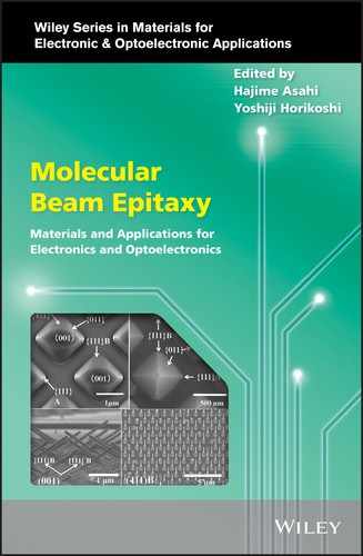
Hashimoto et al. [11] also grew both phase‐separated (sample A: Mn concentration = 12%) and non‐phase‐separated (sample B: Mn concentration = 1.4%) GaMnN layers at 750–800 °C by ammonia‐source MBE. Both samples showed small hysteresis in the magnetization vs. magnetic field (M–H) curves at 7–300 K, showing ferromagnetic characteristics. However, no saturation of the curves was observed at low temperatures, indicating paramagnetic properties. As shown in Figure 18.1, the magnetization rapidly decreases with increasing temperature from 7 to 50 K, thereafter decreasing very slowly up to 300 K. The magnetization of sample A probably originates from Mn‐based compounds or alloys, which have TC higher than room temperature, as indicated by the results of X‐ray diffraction (XRD) and Raman scattering measurements [12]. For sample B, clear paramagnetic behavior was observed below 50 K, originating from the incorporation of Mn into GaN. Therefore, the non‐phase‐separated GaMnN also has paramagnetic properties, which is consistent with GaMnN grown by radio frequency molecular beam epitaxy (RF‐MBE) [13], and the phase‐separated GaMnN exhibits ferromagnetism due to the formation of Mn‐based compounds or alloys, probably GaMn compounds (TC > 740 K). This situation seems to be the same as in Ref. 10. Dhar et al. reported detailed structural studies of GaMnN layers grown on 4H‐SiC substrates by ammonia‐source MBE [14]. Their samples are antiferromagnetic, characteristic of a spin‐glass transition below 10 K. The sample containing Mn clusters exhibits ferromagnetic properties above room temperature, which was attributed to Mn clusters in the alloy.

Figure 18.1 Temperature dependence of magnetization for samples A (phase‐separated, Mn = 12%) and B (non‐phase‐separated, Mn = 1.4%). The magnetization rapidly decreases with increasing temperature from 7 to 50 K, thereafter decreasing very slowly up to 300 K.
(Source: After [11].)
From both GaMnN samples A and B, weak PL emission was observed at around 3.35 eV from the GaMnN layer, in addition to the excitonic transition peak at 3.46–3.47 eV from the GaN buffer layer [11]. Well‐established DMSs, GaMnAs and InMnAs, are grown by low‐temperature MBE to avoid phase separation, and this causes non‐observation of PL emission. On the contrary, GaMnN layers were grown at nearly the same temperatures as GaN layers. This high‐temperature growth allows GaMnN to have both magnetic properties and light‐emitting properties.
18.2.2 GaCrN
First‐principles calculations suggested that Cr‐doped GaN exhibits stable ferromagnetism at room temperature [5]. GaCrN epitaxial layers were grown by MBE with an ion‐removal electron–cyclotron–resonance (ECR) radical cell on sapphire (0001) substrates [15]. For GaCrN with Cr concentration of 1.5%, XRD curves showed only diffraction peaks from hexagonal GaCrN (0002) and (0004), as well as sapphire (0006) and (00012), indicating that c‐axis‐oriented hexagonal GaCrN without any secondary phases was obtained. X‐ray absorption fine structure (XAFS) measurements showed that the Cr atoms substituted the Ga sites. On the other hand, for GaCrN with Cr composition of 2%, additional peaks were observed in the XRD curve, indicating that phase separation occurs in this sample.
M–H curves at 7 and 300 K are shown in Figure 18.2. Clear saturation and hysteresis are observed, indicating that the GaCrN layer is ferromagnetic at both temperatures. In contrast to GaMnN, the magnetization of GaCrN decreases only slowly with increasing temperature, as shown in Figure 18.3 [15]. The CaCrN layer grown by electron–cyclotron–resonance molecular beam epitaxy (ECR‐MBE) shows ferromagnetic behavior with Curie temperature higher than 400 K. On the other hand, single‐crystal GaCrN samples were fabricated by adding Cr to a GaN single crystal by the flux method, which showed ferromagnetic TC at 280 K [16]. Zhou et al. prepared GaCrN thin films with and without Si doping by MBE and observed the increase of TC with Si doping [17].
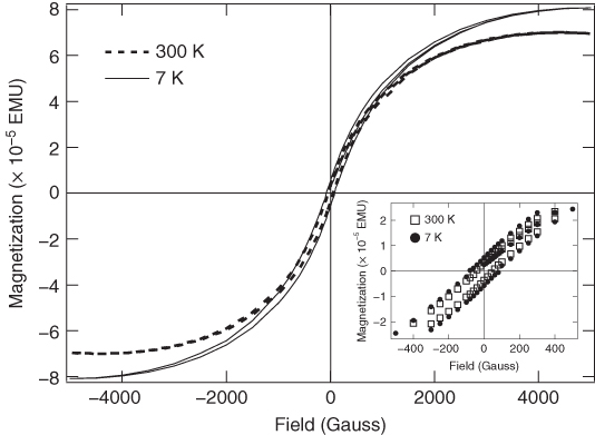
Figure 18.2 M–H curves at 7 and 300 K for the GaCrN sample (Cr concentration = 1.5%). Magnetic field is parallel to the sample plane. The signal from the sapphire (diamagnetic) substrate was extracted.
(Source: After [15].)

Figure 18.3 Temperature variation of magnetization for the GaCrN and GaMnN. Rapid drop at low temperatures, which indicates paramagnetic component, is not observed for the GaCrN.
(Source: After [15].)
PL emission was observed from the grown GaCrN samples (Figure 18.4) [18]. PL peaks were observed at 3.25, 3.27, and 3.29 eV in accordance with Cr doping levels of 0.5%, 1% and 1.5%, as well as at 3.47 eV. These PL peaks are due to free excitonic transitions in cubic GaCrN and hexagonal GaCrN, respectively. This was confirmed by high‐resolution cross‐sectional transmission electron microscopy (TEM) observations: the co‐existence of hexagonal phase and cubic phase [18]. The bandgap of cubic GaN is generally almost 190 meV lower than that of wurtzite GaN. The PL lifetimes for these two peaks were on the order of 0.1 ns. PL emission was also observed even at room temperature [15]. The observation of PL emission from GaCrN will provide novel functional devices to control charges (electrons and holes), spins, as well as photons.
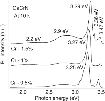
Figure 18.4 10 K PL spectra for the Cr‐doped GaCrN films with different Cr concentrations. The PL peak at 3.25–3.29 eV and that at 3.47 eV are due to the free exciton transitions in cubic GaCrN and hexagonal GaCrN, respectively.
(Source: After [18].)
Enhanced magnetic circular dichroism (MCD) spectra were observed for Si‐doped GaCrN and low‐temperature (300 °C)‐grown non‐doped GaCrN samples; that is the large magneto‐optical effect [19]. On the other hand, almost no MCD signal was observed for the GaN sample without Cr.
18.3 Rare‐Earth‐Doped III‐Nitrides
18.3.1 GaGdN and InGaGdN
18.3.1.1 Magnetic and Optical Properties
GaGdN layers were grown on the (0001) Si face of 6H‐SiC substrates by RF‐MBE [20]. The layer structure was GaGdN(250 nm)/GaN(250 nm)/AlN(20 nm)/SiC. XRD and extended X‐ray absorption fine structure (EXAFS) measurements showed no phase separation and that the Gd atoms occupy the Ga sites. GaGdN layers exhibited n‐type conduction with a relatively high carrier concentration of above 5 × 1019 cm−3 at room temperature.
The M–H curves at 7–300 K showed clear hysteresis curves (Figure 18.5), indicating ferromagnetism [7]. The saturation field was about 2 T and the coercivity Hc was about 70 Oe at 300 K. The magnetization decreased only slowly with increasing temperature and remained even at 400 K, similar to GaCrN in Figure 18.3.

Figure 18.5 M–H curves for the GaGdN sample at several temperatures. The magnetic field is parallel to the sample plane.
(Source: After [7].)
Figure 18.6 shows PL spectra of GaGdN at various temperatures from 10 to 300 K [21]. A broad peak around 500 nm originates from crystal defects. A sharp line at about 650 nm, which shows temperature independence in peak energy, originates from inter‐4f transition of RE ions. The PL decay time of this peak is about 30 μs.

Figure 18.6 PL spectra of GaGdN with a Gd concentration of 6%.
(Source: After [21].)
InGaGdN layers were also grown on metal‐organic vapor‐phase epitaxy (MOVPE)‐grown GaN (0001) template substrates at 400 °C to fabricate long‐wavelength spin‐controlled photonic devices [22]. Figure 18.7 shows room‐temperature PL spectra for InGaGdN layers with different In molar fractions. M–H curves for the InGaGdN single‐layer samples with different Gd concentrations exhibited clear hysteresis and saturation magnetization (MS) at room temperature [23]. The saturation magnetization increased with increasing Gd concentration. With the increase of magnetic Gd atoms, the ferromagnetic interaction increased.
Figure 18.7 Room‐temperature PL spectra taken from the InGaGdN layers of different InN molar fractions (InN 35%, broken line; InN 28%, solid line). Both samples contain ∼1% Gd concentration.
(Source: After [22].)
18.3.1.2 Enhanced Magnetization in LT‐Grown GaGdN
To enhance the magnetization, GaGdN layers were grown at low temperatures from 300 °C to room temperature [ 23–25]. Low‐temperature growth increases the incorporation of Gd concentration without precipitation in the GaGdN layers. The XRD curve for the GaGdN sample with Gd concentration of 12.5% showed only two diffraction peaks from sapphire (0006) and GaGdN (0002), although the peak width was relatively wide, indicating many structural and point defects in the GaGdN layer [24]. On the other hand, a diffraction peak for the GdN (111) was clearly observed from the 700 °C‐grown GaGdN (Gd: 7.8%) sample. XAFS results showed that the majority of Gd atoms substitute the Ga sites in GaN in the low‐temperature‐grown GaGdN layer [25].
Room‐temperature M–H curves for the 300 °C‐grown GaGdN layers with different Gd concentrations are shown in Figure 18.8 [24]. Compared with the 700 °C‐grown GaGdN samples [7], the low‐temperature‐grown GaGdN samples have larger magnetization per unit volume at similar Gd concentration. The magnetic moment per Gd atom of the sample (Gd: 12.5%) is about 6.4μB.
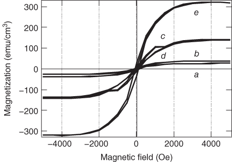
Figure 18.8 Room‐temperature M–H curves for the GaGdN layers grown at 300 °C with different Gd concentrations. Samples a–e are GaGdN with Gd concentrations of 1.8%, 3.0%, 6.5%, 8.9%, and 12.5%, and saturated magnetizations of 26, 38, 142, 138, and 642 emu cm−3, respectively.
(Source: After [24].)
Dhar et al. reported the effect of colossal magnetic moment of Gd and a ferromagnetic‐like behavior with TC above room temperature in Gd‐focused ion‐beam‐implanted GaN [26]. They found that the defects play an important role for ferromagnetism. It is possible that the carriers (electrons) coming from some types of defects, such as nitrogen vacancies, enhanced the ferromagnetism in GaGdN layers.
To study the enhancement of magnetization, Si‐doped and non‐doped GaGdN samples were grown at 300 °C with the same Gd concentration of 8.9% [24]. Clear hysteresis was observed for both samples, and the saturation magnetization of Si‐doped GaGdN is seven times as large as that of non‐doped GaGdN. The saturation magnetization of Si‐doped GaGdN is about 1046 emu cm−3. Co‐doping with Gd and Si is expected to increase the shallow donor density and to enhance the ferromagnetic interaction.
18.3.1.3 Ferromagnetism in Short‐Period SLs
The 230‐nm‐thick GaGdN single‐layer sample and GaGdN/GaN superlattice (SL) samples having nearly the same total thickness of GaGdN (Gd concentration: 1.2%) were grown on sapphire (0001) substrates [27,28]. The magnetization for the SL samples was larger than that for the single‐layer sample. Furthermore, for the SL samples with constant GaN layer thickness of 3.8 nm, the magnetic moment per Gd atom was increased with decreasing GaGdN layer thickness from 2.9 to 1.1 nm. On the contrary, for the SL samples with constant GaGdN layer thickness of 1.3 nm, the magnetic moment per Gd atom is increased with increasing GaN layer thickness from 2.2 to 10.8 nm. Electron carriers in GaN layers flow into and accumulate in the narrower‐bandgap GaGdN layers, resulting in higher electron concentration (>1018 cm−3) in the thinner GaGdN layers. The observed enhanced magnetic moment can be understood by carrier‐mediated ferromagnetism.
Similar enhanced magnetization was also observed on the InGaGdN/GaN SL samples compared with that for the InGaGdN single layer (thickness: 100 nm) [24]. The saturation magnetization was 16 and 7 emu cm−3 for the SL sample and the single‐layer sample, respectively. In the SLs, electron carriers can flow into narrow‐bandgap InGaGdN well layers from the wider‐bandgap GaN layers. These increased carrier concentrations improve the magnetization. However, in the InGaN/GaGdN SL structures the magnetization was decreased [24]. In the InGaN/GaGdN SL structure, carriers (electrons) flow out of the Gd‐containing GaGdN layers and into the narrow‐bandgap InGaN layers. So, the carrier concentrations in the GaGdN layers are decreased, resulting in suppression of the carrier‐mediated magnetization.
18.3.1.4 Large Zeeman Splitting in GaGdN/AlGaN DQW‐SLs
Spin manipulation using circular‐polarized photons and control of the polarization state of emitted light by the spin‐polarized current are based on magneto‐optic effects, including Zeeman splitting. Therefore, studying the magneto‐optic characteristics for nitride‐based DMSs is very important for future optical memories and communications [29,30].
Symmetric GaGdN/AlGaN and GaN/AlGaN double‐quantum‐well superlattices (DQW‐SLs) with Gd concentration of 2% and quantum well (QW) widths of 1 or 2 nm were grown by RF‐MBE on n‐type GaN (0001) templates [31]. Details of the DQW‐SL samples are described in Table 18.1.
Table 18.1 Details of DQW‐SL samples
Source: After Zhou et al. [31].
| Sample | Description | Periods |
| A | AlGaN(18 nm)/GaGdN(2 nm)/AlGaN(9 nm)/GaGdN(2 nm)/AlGaN(18 nm) | 15 |
| B | AlGaN(18 nm)/GaGdN(1 nm)/AlGaN(9 nm)/GaGdN(1 nm)/AlGaN(18 nm) | 10 |
| C | AlGaN(18 nm)/GaN(1 nm)/AlGaN(9 nm)/GaN(1 nm)/AlGaN(18 nm) | 10 |
PL spectra showed two peaks from GaGdN DQWs and the GaN template [31]. With increasing magnetic field from 0 to 7 T, the PL peak (3.586 eV) from the 1‐nm‐thick GaGdN DQWs (sample B) showed a clear shift of about 15 meV to the lower‐energy side, while the peak (3.475 eV) from the GaN template layer showed almost no shift (Figure 18.9). For sample A with 2‐nm‐thick GaGdN DQWs, a redshift of 11 meV was observed. On the contrary, for the GaN/AlGaN DQWs (sample C), almost no shift was observed.
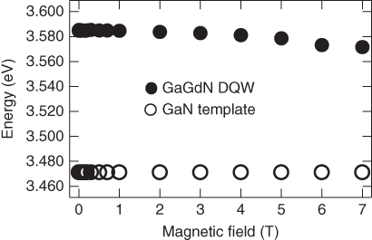
Figure 18.9 Magnetic field dependence of the PL peak energies from GaGdN/AlGaN DQWs (1 nm) and the GaN template for sample B.
(Source: After [31].)
This large redshift in the GaGdN/AlGaN DQW‐SLs indicates a strong enhancement of Zeeman splitting. The g‐factor for sample B was calculated to be about 60 from the magneto‐PL data. Compared with the GaN/AlGaN DQW‐SL sample, this value is huge.
The g‐factor of electrons in a DMS can be described as [32]:

Here, g0 is the g‐factor of the hypothetical material without magnetic ions, and α is the exchange constant for the conduction band. M and B are magnetization and magnetic flux density, respectively. Strong coupling between confined electrons and f electrons of Gd ions in the GaGdN QWs enhances the magnetization and g‐factor.
18.3.2 GaDyN
18.3.2.1 Optical and Magnetic Properties
Dy3+ ion has the largest magnetic moment among RE elements (10.6μB). It is expected that GaDyN will exhibit much larger magnetization and magneto‐optic effect.
GaDyN (210‐nm‐thick) single‐layer and GaDyN/AlGaN multiple‐quantum‐well (MQW) samples were grown on GaN templates by RF‐MBE. The PL spectrum for the GaDyN/AlGaN MQW sample exhibited band‐to‐band emission at around 342 nm from the GaDyN QWs. A sharp emission peak at 581 nm originating from the 4F9/2–6H13/2 transition of Dy3+ [33] was also observed. This sharp peak showed no shift with increasing temperature. This inner‐4f transition suggests that energy transfer from GaN to Dy ions is occurring in the GaDyN wells [34]. The 581 nm emission was also observed in the GaDyN single layer.
Clear hysteresis and saturation were observed for both samples in the magnetization vs. magnetic field curves at room temperature. The saturation magnetization per unit volume of the MQW sample is four times larger than that of the single‐layer sample. This enhancement of magnetization is understood as carrier‐mediated ferromagnetism. In the GaDyN/AlGaN MQW structure, carriers (electrons) flow into narrower‐bandgap GaDyN layers from wider‐bandgap AlDyN layers and are strongly confined in GaDyN wells.
18.3.2.2 Large Magneto‐optical Effect
MBE‐grown GaDyN exhibited significant enhancement of MCD signals compared with MBE‐grown GaN, which suggests that the ferromagnetic properties observed in GaDyN originate from the interaction between the host semiconductor GaN and the doped magnetic ions Dy [35]. The maximum MCD signal value from the GaDyN layer was nine times larger than that from GaN, and large Zeeman splitting was observed at around the bandgap energy of GaDyN. The MCD signal as a function of magnetic field for GaDyN grown at 300 °C showed clear hysteresis [35].
18.3.3 Other RE‐Doped III‐Nitrides
A Ga0.98Eu0.02N sample was grown by ammonia‐source MBE on (0001) sapphire substrate [36–38]. The PL spectra exhibited sharp luminescence due to the intra‐atomic f–f transitions at 622 nm, attributable to the 5D0–7F2 transition of Eu3+. This indicates that the majority of Eu ions take a valence state of 3+ in GaN. EXAFS measurements showed that Eu ions are surrounded by nitrogen atoms with a coordination number of approximately 4 at first‐nearest neighbor, indicating the substitution of Eu ions into Ga lattice sites [38].
The magnetic moment for Ga0.98Eu0.02N saturated at approximately 0.5 T. While at low temperatures the magnetic moment gradually saturated with increasing magnetic field, a clear hysteresis loop was observed at room temperature, indicating the coexistence of two phases: a ferromagnetic‐like phase and a paramagnetic‐like phase [38]. The Curie temperature was above room temperature. It was concluded that the observed paramagnetic and ferromagnetic behaviors are caused by the coexistence of divalent and trivalent Eu ions and the interaction between them. The coexistence of divalent and trivalent Eu ions was confirmed by the observation of the structures from the divalent and trivalent Eu ions in the X‐ray absorption near‐edge structure (XANES) spectrum for the GaEuN sample [39].
Sm‐doped GaN thin films were grown on GaN templates by plasma‐assisted MBE and their structural, optical and magnetic properties were investigated [40]. Reflection high‐energy electron diffraction (RHEED) and XRD measurements showed that the GaSmN films with SmN mole fraction of ∼8% or below have no segregation of any secondary phases. The GaSmN films displayed hysteresis loops in M–H curves at 300 K.
18.4 Device Applications
18.4.1 TMR in GaCrN‐Based Trilayer Structures
TMR device structures were fabricated using the GaCrN (30 nm thick, Cr = 1.0%)/AlN (3 nm)/GaCrN (250 nm, Cr = 2%) trilayer structures grown on MOVPE‐grown n‐GaN (0001) templates grown by RF‐MBE [9].
The magnetic field dependence of tunnel resistance measured with a current of 0.1 μA at 77 K is shown in Figure 18.10. A magnetic field from −2 to 2 kG was applied parallel to the junction plane. Red and blue curves were obtained by sweeping the field from positive to negative and negative to positive, respectively. TMR characteristics were observed. When the field was swept from positive to negative (red curve), the resistance suddenly increased at H = −0.1 kG, where the magnetization in one GaCrN layer reverses and the configuration of the magnetizations in the two GaCrN layers changes from parallel to anti‐parallel. For further decreases of the field, the resistance decreases again to the initial value at H = −0.25 kG, where the magnetization in the other GaCrN layer also reverses and the configuration of the magnetizations in the two layers becomes parallel again. The resistance is higher in the anti‐parallel magnetization regions. The magnetizations in the GaCrN layers become anti‐parallel at H = −0.1 to −0.25 kG (red curve) and H = 0.15 to 0.3 kG (blue curve). The observation of TMR characteristics at 77 K is the highest temperature ever observed for the magnetic tunnel junctions (MTJs) of fully semiconductor‐based DMS and epitaxial heterostructures. However, the TMR ratio was only 0.1%.

Figure 18.10 TMR curves at 77 K for the trilayer sample. Red and blue curves were obtained by sweeping the magnetic field from positive to negative and negative to positive, respectively. Dotted horizontal arrows show the sweep directions of the magnetic field. Horizontal arrows in the trilayer structures show the directions of spin in each magnetic field region, indicated by numbers 1–4.
(Source: After [9].)
18.4.2 Interlayer Interaction Between GaDyN Layers
The magnetization reversal using the GaMnAs‐based double‐barrier magnetic tunnel junctions (DB‐MTJs) was realized by a low current density [41]. Current‐driven magnetic orientation reversal at an extremely low threshold current density, as low as 2.0 × 10⁴ A cm−2, has been achieved in GaMnAs‐based DB‐MTJs sandwiched between top and bottom MTJs. The middle magnetic free layer thickness dependence clearly demonstrated that the low threshold current density is owing not only to the small magnetization of the magnetic free layer, but also the enhancement of the spin torque caused by a spin‐polarized current through the top and bottom MTJs [41]. RE‐doped GaN shows very high Curie temperatures above room temperature [ 7,42,43], and these materials have attracted much attention as DB‐MTJs materials.
GaDyN/GaN DB‐MTJs structures were grown on GaN templates by RF‐MBE. Figure 18.11 illustrates the saturation magnetization and the coercivity versus the middle magnetic layer thickness for the GaDyN/GaN DB‐MTJs samples, respectively. With increasing thickness of the middle magnetic layer, the in‐plane and out‐of‐plane saturation magnetization and the coercivity show opposite behavior. This phenomenon suggests that interlayer interaction exists in the GaDyN/GaN DB‐MTJs structure at room temperature.

Figure 18.11 (a) Saturation magnetization for the GaDyN/GaN DB‐MTJs samples and (b) their coercivity as a function of middle magnetic layer thickness. Circles and triangles indicate the magnetic field applied in‐plane and perpendicular to the sample surface, respectively.
18.4.3 CP‐LD and Other Spintronic Device Applications
CP‐LDs are important devices to realize optical communication systems that are resistant to wiretapping. Holub et al. [44] reported the fabrication of CP‐LD using a vertical‐cavity surface‐emitting laser (VCSEL) structure with GaMnAs DMS layer as spin‐polarized carrier (hole)‐supplying layer and the observation of circular‐polarized light at low temperature of 80 K because of the low TC of GaMnAs. To fabricate practical CP‐LDs, room‐temperature ferromagnetic DMS is a requisite.
Figure 18.12(a) shows a schematic illustration of the CP‐LDs, where the cladding layer or active layer of the LD is replaced with the DMS layer. As shown in Figure 18.12(b), when the spin‐polarized electrons are recombined with holes, circular‐polarized light is emitted and circular‐polarized laser operation is realized. Figure 18.13 shows a schematic illustration of the TMR device consisting of DMS layers and a tunnel barrier layer. This device acts as a circular‐polarized light‐controlled TMR device. When the circular‐polarized light is incident, the spin direction of the DMS layer is changed according to the direction of the circular‐polarized light. This process is the inverse of that in Figure 18.12(b). The combination of these two devices acts as an information processing system.

Figure 18.12 (a) Schematic illustration of the circular‐polarized laser diode. (b) Recombination process of the spin‐polarized carriers leading to circular‐polarized light emission.

Figure 18.13 Schematic illustration of the circular‐polarized light‐controlled TMR device.
CP‐LED (spin LED) was fabricated using MOVPE‐grown Gd‐doped GaN [45]. The InGaN/GaN MQW active layer was sandwiched with Si‐doped n‐type and Mg‐doped p‐type GaGdN cladding layers. The fabricated LED exhibited room‐temperature spin‐polarized electroluminescence, controllable through an applied magnetic field in the Faraday configuration. Additionally, polarization hysteresis was observed, with the spin‐LED retaining 9.3% spin polarization at zero applied field after being exposed to a magnetic field of 5 kG.
Spin injection was also demonstrated from GaCrN in the MBE‐grown GaN‐based spin‐LED [46]. The remanent in‐plane magnetization of the thin‐film semiconducting ferromagnet was used to introduce spin‐polarized electrons into the InGaN quantum well. A saturation circular polarization of ∼2.5% was obtained at 200 K.
18.5 Summary
In this chapter, the MBE growth and characterization of TM‐ and RE‐doped GaN‐based magnetic semiconductors were described. Substitutional incorporation of TM and RE atoms and no phase separation were confirmed by XRD and XAFS measurements. Clear hysteresis and saturation were observed in the magnetization vs. magnetic field curves at room temperature. PL emission was observed from III‐nitride DMSs. Sharp PL emission related to inner‐4f transition was observed from RE‐doped GaN. Carrier‐mediated ferromagnetism was observed in Si co‐doping of GaGdN, and also in GaGdN/AlGaN, InGaGdN/GaN SL, and GaDyN/AlGaN MQW structures. Enhancement of Zeeman splitting was observed in GaGdN/AlGaN DQW‐SL samples. Interlayer interaction was confirmed between the GaDyN thin layers in the GaDyN/GaN DB‐MTJ samples. Finally, examples of spintronic semiconductor devices, where the relation between the spin‐polarized carriers and the circular‐polarized light is used, and the present status to realize such devices were described.
References
- 1 Koshihara, S., Oiwa, T., Hirasawa, M. et al. (1997). Phys. Rev. Lett. 78: 4617.
- 2 Ohno, H., Chiba, D., Matsukura, F. et al. (2000). Nature 408: 944.
- 3 Chen, L., Yang, X., Yang, F. et al. (2011). Nano Lett. 11: 2584.
- 4 Dietl, T., Ohno, H., Matsukura, F. et al. (2000). Science 287: 1019.
- 5 Sato, K. and Katayama‐Yoshida, H. (2001). Jpn. J. Appl. Phys. 40: L485.
- 6 Hashimoto, M., Zhou, Y.K., Kanamura, M., and Asahi, H. (2002). Solid State Commun. 122: 37.
- 7 Teraguchi, N., Suzuki, A., Nanishi, Y. et al. (2002). Solid State Commun. 122: 651.
- 8 Li, X.J., Zhou, Y.K., Kim, M. et al. (2005). Chin. Phys. Lett. 22: 463.
- 9 Kim, M.S., Zhou, Y.K., Funakoshi, M. et al. (2006). Appl. Phys. Lett. 89: 232511.
- 10 Sonoda, S., Shimizu, S., Sasaki, T. et al. (2002). J. Cryst. Growth 237–239: 1358.
- 11 Hashimoto, M., Zhou, Y.K., Tampo, H. et al. (2003). J. Cryst. Growth 252: 499.
- 12 Hasuike, N., Fakamura, H., Harima, H. et al. (2004). J. Phys. Condens. Matter 16: S5811.
- 13 Kondo, T., Kuwabara, S., Oiwa, H., and Munekata, H. (2002). J. Cryst. Growth 237: 1353.
- 14 Dhar, S., Brandt, O., Trampert, A. et al. (2003). Appl. Phys. Lett. 82: 2077.
- 15 Hashimoto, M., Tanaka, H., Emura, S. et al. (2004). J. Cryst. Growth 273: 149.
- 16 Park, S.E., Lee, H.J., Cho, Y.C. et al. (2002). Appl. Phys. Lett. 80: 4187.
- 17 Zhou, Z.P., Yang, Z.X., and Liu, C. (2015). J. Magn. Magn. Mater. 374: 564.
- 18 Shanthi, S., Hashimoto, M., Zhou, Y.K. et al. (2005). J. Appl. Phys. 98: 013526.
- 19 Zhou, Y.K., Fan, P.H., Emura, S. et al. (2012). Phys. Status Solidi C 9: 719.
- 20 Teraguchi, N., Suzuki, A., Saito, Y. et al. (2001). J. Cryst. Growth 230: 392.
- 21 Zhou, Y.K., Kim, M.S., Li, X.J. et al. (2004). J. Phys. Condens. Matter 16 (48): S5743.
- 22 Asahi, H., Hasegawa, S., Zhou, Y.K., and Emura, S. (2012). J. Lumin. 132: 3136.
- 23 Tawil, S.N.M., Krishnamurthy, D., Kakimi, R. et al. (2011). J. Cryst. Growth 323: 351.
- 24 Zhou, Y.K., Choi, S.W., Emura, S. et al. (2008). Appl. Phys. Lett. 92: 062505.
- 25 Zhou, Y.K., Choi, S.W., Kimura, S. et al. (2007). J. Supercond. Novel Magn. 20 (6): 429.
- 26 Dhar, S., Kammermeier, T., Ney, A. et al. (2006). Appl. Phys. Lett. 89: 062503.
- 27 Choi, S.W., Zhou, Y.K., Kim, M.S. et al. (2006). Phys. Status Solidi A 203: 2774.
- 28 Zhou, Y.K., Choi, S.W., Kimura, S. et al. (2010). Thin Solid Films 518: 5659.
- 29 Basu, D., Saha, D., Wu, C.C. et al. (2008). Appl. Phys. Lett. 92: 091119.
- 30 Akinaga, H., Miyanishi, S., Tanaka, K. et al. (2000). Appl. Phys. Lett. 76: 97.
- 31 Zhou, Y.K., Almokhtar, M., Kubo, H. et al. (2012). Solid State Commun. 152: 1270.
- 32 Winter, A., Pascher, H., Hofmaye, M. et al. (2009). Rev. Adv. Mater. Sci. 20: 92.
- 33 Lozykowski, H.J., Jadwisienczak, W.M., and Brown, I. (1999). Appl. Phys. Lett. 74: 1129.
- 34 Kawasaki, T., Nishikawa, A., Furukawa, N. et al. (2010). Phys. Status Solidi C 7: 2040.
- 35 Zhou, Y.K., Emura, S., Hasegawa, S., and Asahi, H. (2011). Phys. Status Solidi C 8: 2173.
- 36 Morishima, S., Maruyama, T., and Akimoto, K. (2000). J. Cryst. Growth 209: 378.
- 37 Morishima, S., Maruyama, T., Tanaka, M. et al. (1999). Phys. Status Solidi A 176: 113.
- 38 Bang, H., Morishima, S., Li, Z. et al. (2002). J. Cryst. Growth 237–239: 1027.
- 39 Tanaka, H., Hashimoto, M., Emura, S. et al. (2003). Phys. Status Solidi C 0: 2864.
- 40 Dehara, K., Miyazaki, Y., and Hasegawa, S. (2016). Jpn. J. Appl. Phys. 55: 5S.
- 41 Watanabe, M., Okabayashi, J., Toyao, H. et al. (2008). Appl. Phys. Lett. 92: 082506.
- 42 Hite, J.K., Thaler, G.T., Khanna, R. et al. (2006). Appl. Phys. Lett. 89: 132119.
- 43 Zavada, J.M., Nepal, N., Ugolini, C. et al. (2007). Appl. Phys. Lett. 91: 054106.
- 44 Holub, M., Shin, J., Chakrabarti, S., and Bhattacharya, P. (2005). Appl. Phys. Lett. 87: 091108.
- 45 A.G. Melton, T. Zaidi, M. Jamil, T. Xu, and I. T. Ferguson, Abstracts of the 9th International Conference on Nitride Semiconductors, #E4‐3 (Glasgow, UK, 2011).
- 46 Banerjee, D., Adari, R., Sankaranarayan, S. et al. (2013). Appl. Phys. Lett. 103: 242408.