26
Molecular Beam Epitaxy for Oxide Electronics
Abhinav Prakash and Bharat Jalan
Department of Chemical Engineering and Materials Science, University of Minnesota – Twin Cities, Minneapolis, MN 55455, USA
26.1 Introduction
Metal oxides are the most abundant of all compounds found on Earth, many of which serve as ores for the extraction of pure elements. Initially thought to be passive, oxides are now ubiquitous, finding applications in numerous hand‐held electronic devices – either in the form of display screens or gate dielectrics in transistors. These oxides can be binary (AmOx), ternary (AmBnOx), or quaternary. Some of the commonly used binary oxides include silicon dioxide (SiO2) in field‐effect devices [1] and indium–tin oxide (ITO) as transparent conductors [2]. Over the years, beta‐gallium oxide (β‐Ga2O3) has also become popular, owing to its wide bandgap, high room‐temperature electron mobility, and high breakdown voltage [3,4]. Ternary oxides, on the other hand, like barium titanate or lead–zirconium titanate, find applications in transducers due to their piezoelectric properties [5,6]. Recently, alkaline earth stannates have garnered much interest due to their optical transparency, wide bandgap, and high conductivity at room temperature [7–9].
26.2 Structure–Property Relationship in Perovskite Oxides
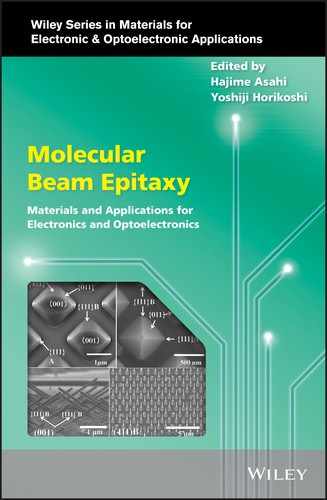
Among various oxides, one class of materials that has emerged as being of great importance is perovskite oxides. These compounds have a general chemical formula of ABO3, where the A‐site is usually occupied by alkaline‐earth (Ca, Sr, Ba, etc.) or rare‐earth elements (La, Gd, Nd, etc.) and the B‐site by transition metals (Ti, Mn, Ru, etc.) or some of the p‐block elements (Al, Sn, Ga, etc.). They have a simple crystal structure, wherein the A‐site refers to the corners of a unit cell and the B‐site refers to the body‐centered position. Six oxygen ions that sit at the face centers form a three‐dimensional network of BO6 octahedra, as illustrated in Figure 26.1. The stability of the crystal is given by Goldschmidt's tolerance factor [10]:

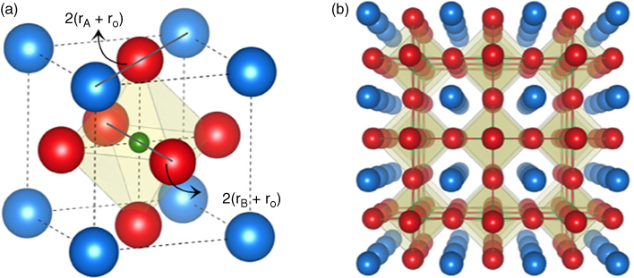
Figure 26.1 (a) A perovskite unit cell, where A atoms (blue) are present at the corners, B (green) at the body center, and O (red) at face centers; (b) perovskite oxides seen as a three‐dimensional network of BO6 octahedra.
where rA, rB, and rO are ionic radii of elements A, B, and oxygen. For the perovskite structure to be stable, t should typically lie between 0.8 and 1.1. A broad range of acceptable tolerance factors that hold the atomic arrangement suggests that the BO6 octahedra can withstand a large amount of strain. The crystal prefers to be cubic if the tolerance factor is close to 1 [11,12]. Deviations in t can occur due to differences in ionic radii of various cations that can be accommodated in the perovskite structure [13]. As t starts to deviate from 1, the structure undergoes symmetry‐lowering changes and no longer remains cubic. These structural changes can exist in the form of octahedral tilts, or distortions, or both [14]. Octahedral tilts and distortions lead to changes in the bond lengths and the B–O–B bond angle, which in turn affects the orbital overlap and hence the bandwidth. Bandwidth W, being coupled with the electronic structure, has a strong influence on the properties of perovskite oxides. In addition to the flexibility provided by the crystal structure, there are several other degrees of freedom that can be exploited to engineer the physical properties of the system.
26.2.1 Lattice Degrees of Freedom
26.2.1.1 Point Defects
Due to their flexible structure, perovskite oxides can adapt to a combination of cation oxidation states if the charge‐neutrality condition is satisfied (sum of the oxidation states for cations = 6). Further modifications to the crystal and electronic structures of perovskite oxides can be achieved by alloying or doping at the A or B‐sites. Structural changes are discernible in oxides when they are alloyed above a certain limit due to changes in the tolerance factor. Lattice parameters of the alloyed compound can vary linearly between the two parent compounds following Vegard's Law. However, Vegard's Law is not strictly followed, with deviations observed in alloyed compounds such as Sn‐alloyed SrTiO3 [15] or Sr‐alloyed BaSnO3 [16]. Doping concentrations, on the other hand, are usually smaller to cause global structural changes. But, aliovalent substitutional doping introduces extra electrons or holes in the lattice, resulting in discernable changes to the electronic structure. Depending on whether the dopant acts as an acceptor or donor, p‐type (hole) or n‐type (electron) carrier transport can be observed, respectively. For instance, in SrTiO3, p‐type conduction is observed if it is doped with Sc on the B‐site, whereas La doping at the A‐site results in electronic transport [17,18]. Some of the oxides can also withstand oxygen vacancies to a certain extent, which provides another route to alter the electronic properties. This is one of the simplest ways of making a film conducting, as creating oxygen vacancies only requires heating the material to high temperatures in moderate vacuum. At such temperatures, oxygen diffuses out of the lattice and leaves as molecular oxygen. It can be visualized from a simple defect reaction, which also shows that oxygen vacancies can dope the material with electrons [19]:
The ability to create oxygen vacancies in a perovskite structure depends on the activation energy associated with the formation of oxygen vacancies and the oxygen diffusion coefficient [20]. For instance, in BaSnO3, although the enthalpy of vacancy formation is low [21], the oxygen diffusion coefficient is known to be orders of magnitude smaller than other perovskite oxides such as SrTiO3 [22], which makes the creation of oxygen vacancies in BaSnO3 relatively difficult. In many oxides, mainly those having high oxygen diffusivity, oxygen vacancies can be suppressed by annealing in oxygen atmosphere at high temperatures [23,24].
26.2.1.2 Strain
When perovskite oxides exist in the form of thin films, strain provides another tuning knob for controlling their properties. The availability of commercial substrates with lattice parameters close to many of the perovskite oxides makes the growth of single‐crystalline, epitaxial thin films possible. Below a critical thickness, films can grow commensurately (completely strained), taking the in‐plane lattice parameter of the underlying substrate. The constraint induced by the substrate can play important roles and can affect the structural, electronic, and magnetic properties significantly. Structurally, substrate‐induced strain and coupling effects have been observed to affect the octahedral tilts in perovskite oxides such as LaNiO3 [25], for instance. In the case of SrTiO3, which is an incipient ferroelectric, tensile strain can stabilize the ferroelectric phase even at room temperature [26].
26.2.1.3 d‐Orbital Splitting
Many of the perovskite oxides are transition‐metal oxides (TMOs), where the B‐site is occupied by transition metals. The physical and electronic properties in TMOs are mostly governed by the electrons in the d‐orbitals. Due to the directional nature of d‐orbitals and the system's propensity to minimize the total energy, several other effects have been observed that are unique to TMOs. Therefore, it is important to review some of the factors relevant to TMOs, such as crystal field splitting, Hund's coupling, and Jahn–Teller distortion. Crystal field splitting in TMOs refers to the splitting of the otherwise degenerate d‐orbitals into different energy levels in the presence of the crystal's static electric field, as shown in Figure 26.2. In the octahedral coordination geometry of the perovskite structure, ![]() and
and ![]() orbitals (called eg orbitals) are directed toward the oxygen ions and therefore electrons in these orbitals experience greater coulombic repulsion. This increases their energies relative to the other three dxy, dyz, and dxz orbitals (called t2g orbitals). The energy difference between the eg and t2g orbitals is called the crystal field splitting parameter (Δo). When filling these orbitals, electrons first occupy the lower‐energy t2g orbitals. Once all three orbitals are filled with one electron each, Δo prevents the occupancy of higher‐energy eg orbitals and favors pairing of electrons with opposite spins. The overall spin angular momentum is therefore reduced in such a configuration. This is known as the low‐spin state. However, when electrons with opposite spins are paired, there exists an energy penalty called the Hund's rule coupling energy (Hex) due to electrostatic repulsion. When Hex > Δo, it is energetically favorable for the electrons to occupy eg orbitals before pairing with t2g electrons, thus maximizing the total spin angular momentum (Hund's Rule). This configuration is known as the high‐spin state. The ground state in TMOs, therefore, may result from a competition between crystal field splitting and Hund's coupling. When Hex and Δo are comparable, the electronic and magnetic properties of TMOs can be tuned by driving the system from a low‐spin ground state to a high‐spin state or vice versa.
orbitals (called eg orbitals) are directed toward the oxygen ions and therefore electrons in these orbitals experience greater coulombic repulsion. This increases their energies relative to the other three dxy, dyz, and dxz orbitals (called t2g orbitals). The energy difference between the eg and t2g orbitals is called the crystal field splitting parameter (Δo). When filling these orbitals, electrons first occupy the lower‐energy t2g orbitals. Once all three orbitals are filled with one electron each, Δo prevents the occupancy of higher‐energy eg orbitals and favors pairing of electrons with opposite spins. The overall spin angular momentum is therefore reduced in such a configuration. This is known as the low‐spin state. However, when electrons with opposite spins are paired, there exists an energy penalty called the Hund's rule coupling energy (Hex) due to electrostatic repulsion. When Hex > Δo, it is energetically favorable for the electrons to occupy eg orbitals before pairing with t2g electrons, thus maximizing the total spin angular momentum (Hund's Rule). This configuration is known as the high‐spin state. The ground state in TMOs, therefore, may result from a competition between crystal field splitting and Hund's coupling. When Hex and Δo are comparable, the electronic and magnetic properties of TMOs can be tuned by driving the system from a low‐spin ground state to a high‐spin state or vice versa.
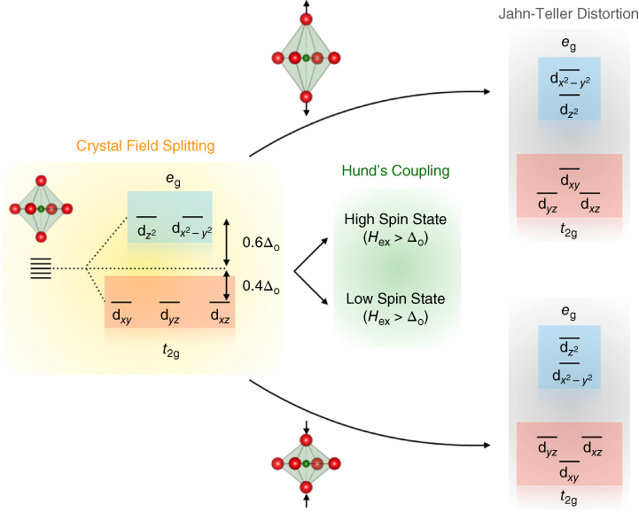
Figure 26.2 Crystal field splitting, Hund's coupling, and Jahn–Teller distortion can lead to different ground states in transition metal oxides.
For certain electronic configurations, perovskite oxides can further lower their total energy by undergoing Jahn–Teller distortions. These distortions are accompanied by splitting of the eg and t2g orbitals, further depending on the type of distortion (elongation vs. compression), as depicted in Figure 26.2. Since two electrons with different spin can occupy d orbitals, degeneracy can further be lifted in TMOs where strong spin–orbit coupling exists.
Several degrees of freedom, discussed above, provided by the amenable crystal structure of perovskite oxides are responsible for the existence of a wide range of novel functionalities. Some of the intriguing properties that have been discovered include high‐temperature superconductivity (e.g. BaxLa5−xCu5O5(3−y)) [27], room‐temperature ferromagnetism (e.g. La0.7Sr0.3MnO3) [28], multiferroicity (e.g. BiFeO3, BiMnO3) [29,30], colossal magnetoresistance (e.g. La0.67Ca0.33MnO3) [31], and so on.
26.2.2 Interfacial Physics
Besides a diverse range of fascinating properties in bulk or thin films, new interfacial phenomena continue to unfold in heterostructures of perovskite oxides. A big impetus to the study of interfacial properties and physics came with the realization of two‐dimensional electron gas (2DEG) at the LaAlO3/SrTiO3 interface in the year 2004 [32]. The existence of a conducting 2D layer between two band insulators was attributed to the polar discontinuity resulting in electronic reconstruction at the interface [32]. Following the seminal work of Ohtomo and Hwang, many interfacial properties and novel physics were identified, including superconductivity [33–35], ferromagnetism [36–41], quantum Hall effects [42,43], ferroelectricity [44], charge transfer via broken‐gap junction [45], and so on, which are otherwise absent in the parent oxide layers. Superconductivity and ferromagnetism have even been shown to coexist at such interfaces [46]. Furthermore, these properties can be tailored with external parameters such as strain effects, electric or magnetic fields [47–52]. New physics and properties are not just limited to interfaces, but can be realized even in superlattices and heterostructures [53–57].
The observation of novel ground states unique to thin films and heterostructures has been made possible with the ability to produce films with abrupt interfaces, and controlled defect densities. Even after more than five decades of existence of thin‐film growth techniques, they continue to mature. Recent demonstration of two‐dimensional hole gas at the LaAlO3/SrTiO3 interface is a good example [58]. Growth approaches available today are capable of precisely varying the thickness of films to atomic‐layer precision [59–61]. Properties in thin films and heterostructures are, however, found to be extremely sensitive to stoichiometry, defects, interfacial roughness, surface termination, thickness, and so on [62,63]. For example, the 2DEG that was first observed in the LaAlO3/SrTiO3 heterostructure only forms if the SrTiO3 substrate has a TiO2‐termination. LaAlO3 films grown on SrO‐terminated substrate were found to be insulating [64]. In addition to surface termination, cation stoichiometry also has a strong influence on the properties of 2DEG [ 6265–67]. For example, La‐rich LaAlO3 films have been shown to result in non‐conducting LaAlO3/SrTiO3 interfaces [66,68,69]. For intrinsic physics studies and the discovery of novel phenomena, it is thus critical to have both good structural quality and excellent control over the point defects in thin films grown using ultra‐high vacuum (UHV) deposition techniques [70]. The following section will review some of the common thin‐film growth techniques employed today, and compare their advantages and disadvantages.
26.2.3 Thin‐Film Growth Approaches
Thin‐film growth techniques for oxides can be classified into two broad categories – solution and vapor‐based approaches.
26.2.3.1 Solution‐Phase Synthesis
Solution‐phase methods are perhaps the oldest known way of depositing films on a substrate. This is illustrated in Figure 26.3. In step 1, a mixture of solutes is first dispersed in a solution to form colloids, also known as precursors. The solutes react with each other during the aging step, either at room temperature or moderately high temperature, to form the desired material to be deposited. In step 2, the precursor is then transferred to the substrate using a coating technique such as spin‐coating or dip‐coating. The next step involves removal of the liquid phase, either by baking at high temperature or using a centrifuge. This leaves a layer of film on the substrate, which is usually amorphous. Annealing at high temperature improves the crystallinity of the films, however, grain boundaries exist with grain sizes on the order of a few nanometers. These steps can be repeated to achieve a desired thickness of the film. The simplicity with which films can be deposited with this approach makes it one of the most popular, cost‐effective, and energy‐efficient thin‐film deposition methods, albeit not providing atomic‐layer control over film thickness, with the properties being limited by structural imperfections such as grain boundaries and impurity in solutes [71].

Figure 26.3 Schematic showing a typical sol‐gel method for producing thin films.
Source: Adapted from Ref. [71].
26.2.3.2 Vapor‐Phase Synthesis
Vapor‐phase deposition techniques differ from solution‐based approaches in a way that involves a phase change, where the starting material (originally existing as a solid or liquid) is transformed to vapors before encountering the substrate. Vapor deposition can be further classified into chemical and physical deposition approaches. Chemical deposition includes a chemical reaction taking place at the surface of the substrate, whereas in physical deposition methods, films are directly transferred onto the substrate by evaporation or sublimation. Three of the widely used physical vapor deposition methods are discussed below.
26.2.3.2.1 Sputtering
In sputtering, the source material is a bulk sintered target of the film that is being deposited on a substrate. Sputtering of the target is carried out using a plasma source – typically a mixture of an inert gas like argon with oxygen for oxide materials. The ionized species of plasma with positive charges bombard the surface of the target, removing some of the material. The materials coming off the target are also charged and travel toward the substrate due to the applied potential difference between the target and the substrate. The voltage difference can be either DC or AC, depending on the electrical property of the target. Insulating targets require an AC source to avoid charge build‐up at the surface, which would suppress the kinetic energy with which the ionized plasma travels toward the target [72]. Cost‐effectiveness and high throughput of sputter deposition make it one of the preferred industrial growth techniques. However, there are certain challenges, including high defect densities that limit the study of intrinsic properties of thin films.
26.2.3.2.2 Pulsed Laser Deposition
Pulsed laser deposition (PLD) is similar to the sputtering approach, except that instead of an argon plasma, a laser beam is used to ablate the target [73]. The target material should have a high optical absorption coefficient at laser wavelength. Due to ionization by the high‐energy laser beam, the material creates its own plasma, which is directed toward the substrate. The flux of the plume is responsible for film deposition. The film growth can be controlled using the laser pulse. The growth rate is dependent on the laser energy, distance between the substrate and the target, and the background gas pressure. By proper choice of these parameters, each laser pulse can be used to deposit a submonolayer of material at a time. Growth rates are typically below 1 Å per pulse. PLD is usually equipped with in‐situ reflection high‐energy electron diffraction (RHEED), which helps in monitoring the surface crystallinity and growth mode. RHEED intensity oscillations can provide information about the growth rate also for layer‐by‐layer growth [74].
Sputtering and PLD have been used to create some of the structurally superior‐quality thin films and heterostructures with properties not observable in films grown with solution‐based approaches [ 32, 42]. One of the main advantages of sputtering and PLD is their applicability to a wide range of materials. The processes are cheap and can be scaled up to meet industry requirements. In both these methods, the stoichiometry of the target can be preserved (“congruent material transfer”) under proper choice of growth conditions. However, if laser fluence is not selected appropriately, stoichiometry has been found to vary considerably during PLD growth [75]. Even for the same growth parameters, sample‐to‐sample variation has been observed. Sputtering and PLD are both high‐energy deposition techniques, where the high kinetic energy of particles leaving the target can re‐sputter the film. The re‐sputtering effect can create defects which are deleterious to the properties of the films. This can, however, be minimized by a modified sputtering technique called high‐pressure sputtering, in which the oxygen is supplied at relatively high pressure to decrease the kinetic energy of the particles [76–78]. Film properties are also limited by the composition control and purity of the target [79,80]. Sometimes single‐crystalline targets are used to overcome this issue, which, however, increases the total cost of production [81].
26.2.3.2.3 Molecular Beam Epitaxy
In the late 1960s, another thin‐film growth technique known as molecular beam epitaxy (MBE) was devised by A. Y. Cho and J. R. Arthur, which overcame some of the challenges with other deposition methods [82–84]. MBE is a low‐energy, UHV thin‐film deposition technique which employs a molecular beam of source materials impinging at the substrate kept at high temperature. Molecular beam means that the mean free paths of atoms or molecules are larger than the source‐to‐substrate distance (due to the UHV environment). As a result, no inter‐atomic/molecular collision occurs before they reach the substrate. High temperature promotes formation of single‐crystalline films. MBE can be thought of as a combination of chemical and physical vapor deposition, where individual species are either evaporated using an effusion Knudsen cell or an electron beam. These species react with each other to form a layer of material at the surface of the substrate. MBE offers atomic‐layer control over film composition, thickness, and roughness. Films can be grown with low defect densities due to the molecular growth regime. MBE also comes equipped with other in‐situ tools in addition to RHEED, such as a quartz crystal microbalance (QCM) and/or beam flux monitor (BFM), to precisely control the flux of individual beams for better stoichiometry control [83,85,86].
26.3 Oxide Molecular Beam Epitaxy
26.3.1 Historical Perspective
The first demonstration of oxide MBE dates back to 1978, when Hirose, Fischer, and Ploog [87,88] used a molecular oxygen source for the growth of amorphous aluminum oxide (Al2O3) on gallium arsenide (GaAs) film to make a metal–oxide–semiconductor (MOS) heterostructure. One of the challenges associated with the growth of oxide on conventional semiconductors such as GaAs was the incorporation of oxygen in the semiconductor lattice. In this case, it was found that the stoichiometry of the underlying GaAs layer was modified in the presence of oxygen. Even with the insertion of an Al0.5Ga0.5As layer between Al2O3 and GaAs to prevent oxidation of GaAs, oxygen diffusion was found to be an issue due to relatively high growth temperatures. Lower growth temperatures, on the other hand, would reduce the reactivity of oxygen remarkably. To strike a balance between the two, more efficient oxygen sources were desirable [87], but were not implemented in MBE growth until 10 years later, due to compatibility issues, as we discuss later.
The first growth of ternary oxides was reported in 1982–1983 by Stall [89], who used volatile oxides (As2O3 and Sb2O3) as a source of oxygen to grow amorphous spinel Al2MgO4, but it was not until 1985 that the first crystalline ternary oxide (LiNbO3) was grown [90]. Major advancements in the development of oxide MBE came after the discovery of high‐temperature superconductivity in copper‐based oxides (cuprates) [ 2791–96]. Thin films grown using MBE with molecular oxygen were, however, amorphous and showed no sign of superconductivity. Long post‐growth anneals at high temperatures and high oxygen pressures were required to make films crystalline and to stabilize the superconducting phase [97]. To utilize the full advantages of MBE over other growth techniques such as atomic‐layer control and ability to grow uninterrupted superlattice structures with smooth interfaces, controlling the properties of the films in‐situ was desirable. This was achieved by integrating more efficient oxygen sources such as oxygen plasma [98,99] and ozone [100,101] with MBE. With the use of more reactive oxygen sources, the post‐growth annealing step was largely eliminated.
26.3.2 Design of Oxide MBE
26.3.2.1 Oxygen Plasma‐Assisted MBE
Figure 26.4(a) shows a typical design of a radio‐frequency (rf) plasma source consisting of a water‐cooled rf coil inductively coupled with the rf source operating at 13.56 MHz. It is supplemented with an external matching unit for optimum plasma coupling and to minimize the reflected power. The efficiency of plasma sources is argued to vary anywhere between 10% and 70%, depending on the choice of oxygen pressure and plasma power [Figure 26.4(b)] [102]. Additionally, rf plasma sources are often equipped with ion deflection plates to prevent electrons and high‐energy ions from reaching the growth surface. An atomic source of oxygen has also proved effective in substrate cleaning prior to growth, and to remove any carbon contamination from the surface [103,104]. This ensures that the interface between the film and the substrate is clean, which is essential for studying novel interfacial phenomena.
Figure 26.4 (a) Schematic of the rf plasma source in Jalan's MBE laboratory at the University of Minnesota; (b) dissociation efficiencies of an rf plasma as a function of gas pressure and rf power.
Source: Dissociation efficiencies are taken from Ref. [102].
26.3.2.2 Ozone‐Assisted MBE
The ozone delivery system, on the other hand, consists of a silent discharge ozone generator and a temperature‐controlled ozone trap/still (Figure 26.5). Ozone is either stored in the trap in liquid form or adsorbed on silica gel in gaseous form. Silica gel is supposed to be safer, as liquified ozone is prone to explosions due to abrupt changes in temperature. Cases of explosions have been reported even with the use of silica gel due to the presence of a small amount of liquid ozone. A region of flowing nitrogen gas between the trap and the liquid nitrogen panel keeps the temperature above the liquefaction temperature of ozone, and has proved useful in avoiding these explosions [106,107].

Figure 26.5 Schematic of the ozone delivery system.
Source: Reproduced with permission from Ref. [105].
26.3.2.3 NO2 and H2O2 Assisted MBE
Besides molecular oxygen, oxygen plasma and ozone, nitrogen dioxide (NO2) and hydrogen peroxide (H2O2) have been shown to work as oxidizing agents. Growth using NO2 was carried out even at pressures as low as 10−7 Torr [108–111]. However, the reactivity of NO2 was found to be lower than ozone [109]. NO2 is not a preferred oxidant when substitutional defects become detrimental to the properties of thin films [112], due to the incorporation of nitrogen ions at oxygen sites. A H2O2/H2O mixture was also demonstrated to be a good source of oxygen for oxide film growth [113]. Since water vapor is undesirable for UHV synthesis, the use of H2O2/H2O mixtures is limited.
26.3.3 Challenges with Oxide MBE
With oxygen sources, either in the form of molecular oxygen, rf plasma, ozone, NO2, or H2O2/H2O mixtures, practical compatibility issues in a UHV environment need to be considered. In what follows, we discuss potential issues associated with the use of oxygen in MBE, along with possible remedies.
26.3.3.1 Issues with the Substrate Heater Filament
The lifetime of the substrate heater filament, generally operating at high temperature, is severely reduced in the presence of high oxygen pressure. With the introduction of more efficient oxygen sources, although the life span was improved as a result of the use of lower oxygen partial pressure, the operating temperature was still limited by filament oxidation [107]. Nowadays, oxygen‐resistant heater filaments made from SiC or noble‐metal alloys (Ni or Pt) have replaced tungsten filaments in oxide MBE systems to achieve higher operating temperatures. The working temperature of SiC filaments can be as high as 1000 °C, depending on the partial pressure of oxygen during growth. Besides the filaments, shields that prevent radiative loss of heat should be compatible with oxygen. Tantalum and stainless steel are most common. Their performance at high temperature and high oxygen pressure can be further enhanced with coatings of oxidation‐resistant nickel alloys, or by replacing them with Ni‐based alloys such as Inconel. Vapor pressure and cross contaminations are always important considerations in choosing parts consisting of non‐refractory materials.
26.3.3.2 Issues with Substrate Holders and Cell Crucibles
Substrate holders made from molybdenum may oxidize in plasma or ozone. Molybdenum oxides having higher vapor pressure than molybdenum itself can get incorporated in the film, which is undesirable [ 106,114]. This type of contamination can be avoided by choosing holders made of materials that are oxidation‐resistant (such as stainless steel, Inconel alloy, etc.), or materials whose oxides have a much lower vapor pressure (such as tantalum). Use of oxygen‐resistant materials recently led to the discovery of the highest mobility (>106 cm2 V−1 s−1) ever reported in MgZnO/ZnO heterostructures [115]. The choice of crucible should also be considered, in terms of wettability and reactivity with the source material, and reactivity with an oxidizing atmosphere. Pyrolytic boron nitride is a widely used crucible in MBE growth. However, its reactivity in oxygen‐rich environments results in the formation of B2O3, which may contaminate the films [107].
26.3.3.3 Issues with Effusion Cells and Flux Instability
Oxidation of the filaments used in the effusion cell is critical for sources that operate at high temperature. Filament oxidation leads to instability in the flux due to temperature fluctuations, which has undesirable effects on the stoichiometry of the films. Filament materials are, therefore, chosen such that stable fluxes are achievable in high oxygen background. Perhaps an even more severe concern than the filament oxidation is that there is a greater risk of oxidation of the source material in oxide MBE, which again leads to flux instabilities. This issue becomes especially important for high‐oxidation‐potential elements, such as Sr, Ba, Ca, and so on, and for elements with low vapor pressure, such as Ti, Sn, and so on, that require high cell temperatures [116–118]. At high effusion‐cell temperatures, the reactivity of elements with oxygen is enhanced, which can result in oxidation of the charge and flux instability. A significant change in flux is observed when an oxygen source is introduced (Figure 26.6) [ 116,119], due to partial oxidation of the sources. Time‐dependent flux measurements for Ti have shown that flux monotonically decreases in high‐pressure oxygen [117]. This is attributed to the formation of titanium dioxide and its low vapor pressure. In case of ternary oxides, flux instabilities often result in non‐stoichiometric defects. On the other hand, for binary oxides, although stoichiometry can be maintained, lower flux causes a decrease in the growth rate. Growth rates become important when dopants are used, because the doping concentration varies with the growth rate [120].
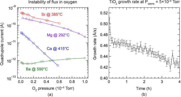
Figure 26.6 (a) Variation in the quadrupole current for Sr, Mg, Ca, and Ba (an indirect measure of flux) at different oxygen pressure. Source: Adapted from Ref. [116]. (b) Changes in the growth rate for titanium oxide as a function of time in an ozone background pressure of 5 × 10⁻⁵ Torr.
Source: Adapted from Ref. [117].
The oxidation of source elements can be minimized, either by use of differential pumping through a port aperture [121], or a crucible aperture to minimize the charge exposure to oxygen environment [122]. The use of a ceramic aperture, however, also decreased the growth rate. For elements that readily oxidize, it is critical to protect them when they are not in use. Retractable effusion cells are designed to prevent oxidation of such elements during venting of the growth chamber or while growing other oxides. Moreover, they also facilitate replacement of charge without breaking the vacuum of the growth chamber.
Flux instabilities due to source or filament oxidation make beam flux calibration very critical in oxide MBE. Popular ways of measuring fluxes include QCM and BFM. These two techniques allow for measuring the growth rate and flux, respectively, directly below the substrate using a linear travel mechanism. While QCM relies on the change in mass of the quartz crystal and can be used with oxygen, BFM is a type of ionization gauge that is prone to oxidation. Therefore, flux measurements using BFM are usually done prior to growth. On the other hand, the quartz crystal in the QCM needs to be replaced more often than the BFM. To overcome these challenges, sometime real‐time flux‐monitoring systems such as atomic absorption spectroscopy are utilized, which improve the accuracy of flux calibration [123].
One of the advantages of MBE is the availability of in‐situ diagnostic tools for surface characterization, such as RHEED. Apart from providing information about the surface morphology, growth modes, and growth rates (for layer‐by‐layer growth mode) [124], RHEED can be used to adjust the fluxes so as to achieve stoichiometric growth conditions [125,126]. It should be noted that RHEED cannot be used as a standalone method for optimizing the stoichiometry, as it is a surface‐sensitive technique. Stoichiometry needs to be simultaneously confirmed by other composition characterization methods such as X‐ray diffraction and Rutherford backscattering spectrometry (RBS), for example. However, during prolonged exposure to oxygen, RHEED filament oxidation is inevitable if proper caution is not taken. One way to minimize the effect of oxygen is by using differential pumping near the filament, which helps in increasing its lifetime.
26.4 Recent Developments in Oxide MBE
26.4.1 Adsorption‐Controlled Growth
The existence of adsorption‐controlled growth in some ternary perovskite oxides helps in eliminating the disadvantages of flux instabilities and unreliability in growth. The first study of adsorption‐controlled growth was reported by Arthur, where the growth of GaAs was studied using MBE [82] following the work of Gunther [127]. Theis and Schlom were the first to demonstrate adsorption‐controlled growth in the perovskite oxide PbTiO3 [128,129]. In this kind of growth mode, non‐stoichiometry resulting from small fluctuations in the beam flux of Pb or Ti is compensated by excess Pb desorbing from the surface in the form of PbO. The deposition rate in the adsorption‐limited regime is determined by the non‐volatile component – in this case TiO2 (Figure 26.7).
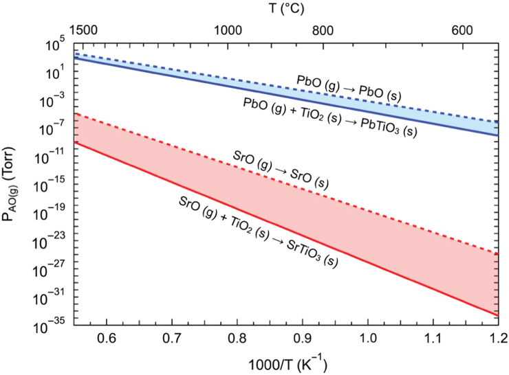
Figure 26.7 Theoretical growth window for PbTiO3 and SrTiO3 assuming a titanium sticking coefficient of 1.
Although adsorption‐controlled growth has been demonstrated for many perovskite oxides including PbTiO3, Bi2Sr2CuOy, Bi4Ti3O12, BiFeO3, BiMnO3, and LuFe2O4 [132–136], to access such a growth regime or “MBE growth window” as it is now called, certain conditions should be satisfied. First, at a given temperature, the equilibrium partial pressure of the volatile oxide should be high enough to enable deposition of perovskite oxide with practically achievable growth rates. Second, the growth window should be accessible at realistic temperatures.
However, it is not possible to satisfy these criteria for all perovskite oxides. For example, in the case of MBE growth of SrTiO3 using solid sources for Sr and Ti, it has been found that a growth window may exist at much lower vapor pressures (in this case SrO), as illustrated in Figure 26.7. To achieve practical fluxes, much higher substrate temperatures are required, which may not be feasible for oxide MBE. Besides an inaccessible growth window, several other challenges exist for the growth of SrTiO3.
- One issue is the low vapor pressure of titanium. As a result, the growth rate of SrTiO3 is limited by titanium. Higher growth rates are required for practical applications.
- Titanium flux is unstable in the presence of oxygen, as previously shown in Figure 26.6(b), which can result in high defect concentrations in the film in the form of cation non‐stoichiometry. Beam fluctuation in the range of 0.1–1.0% can introduce a defect density of ∼1020 cm−3 in films [137].
- To maintain the desired mean free path of atomic species, and due to the limitations put on the system by pumps, oxygen pressure is usually kept low. At the same time, high substrate temperatures are necessary for better crystallinity of films. As a result, oxygen vacancies are prone to form in the film during growth. These oxygen vacancies often tend to make the film conducting, which may be undesirable for some applications such as dielectrics. Post‐oxygen annealing, therefore, becomes necessary, adding an extra processing step. In fact, the post‐oxygen annealing step may or may not work in some cases.
These issues are not just pertinent to titanium, but also apply to other elements that have low vapor pressures (e.g. vanadium, ruthenium, etc.). To achieve a balance between elemental flux stability and the need for high oxygen pressure, an alternative MBE approach was devised, known as hybrid MBE (conventionally known as metal–organic MBE or MOMBE [138,139]).
26.4.2 Hybrid Molecular Beam Epitaxy
As the name suggests, hybrid MBE is a combination of conventional MBE and metal–organic MBE. The method, first introduced by Jalan et al. in 2009 for SrTiO3 films, used a conventional effusion cell for strontium and a metal–organic precursor – titanium tetraisopropoxide (TTIP) – for titanium [ 137,140,141]. TTIP was supplied through a gas inlet system, as illustrated in Figure 26.8. The precursor was thermally evaporated from a stainless‐steel bubbler. The gas lines were maintained at higher temperature than the bubbler to prevent any condensation and subsequent blockage. The pressure of the gas precursor was controlled using a linear leak valve that receives feedback from a capacitive manometer (Baratron®). Unlike metal–organic chemical vapor deposition (MOCVD), no carrier gases were used. The shower head nozzle design of the gas injector provides an effusive beam of TTIP. The way a TTIP precursor works is that at high growth temperatures (>400 °C), it decomposes into TiO2 via the following reaction [143,144], thereby forming TiO2 at the surface of the substrate:

Figure 26.8 Schematic showing (a) conventional MBE setup with both elements supplied through an effusion cell and (b) hybrid MBE setup where one of the effusion cells is replaced by a gas inlet system.
Source: Reproduced with permission from [142].
The hybrid MBE approach offers several advantages over the conventional MBE approach:
- TTIP has a much higher vapor pressure than solid titanium, allowing for growth rates to be scalable. Due to its high vapor pressure, no carrier gas is needed, thereby reducing the load on vacuum pumps [140].
- The beam flux remains stable in the presence of oxygen as the precursor does not come into direct contact with oxygen. This also facilitates refilling the metal–organic source without venting the growth chamber [ 140, 141].
- Since the precursor comes already bonded with oxygen, the oxidation state of Ti is preserved. The use of TTIP with oxygen plasma also helps maintain the oxygen stoichiometry and the insulating nature of SrTiO3 films [141].
- TTIP enables an adsorption‐controlled growth window to be accessible at reasonable growth temperatures [137].
Using this precursor, several perovskite oxides have been grown, including SrTiO3, CaTiO3, and BaTiO3 [ 141,145,146]. Figure 26.9(a–c) shows the out‐of‐plane lattice parameters for SrTiO3 films grown at different Ti:Sr beam equivalent pressure (BEP) ratio and different growth temperatures. For all three temperatures, there was a range of Ti:Sr ratio for which the lattice parameter was identical to the bulk value. This suggested that a self‐regulated growth window exists for SrTiO3 when TTIP is used as a Ti source. With increasing temperature, the lower boundary of the growth window shifted to a higher TTIP flux because of the increased rate of TTIP desorption. Moreover, higher growth temperatures also resulted in broadening of the growth window [148,149]. Outside the growth window, the lattice parameter showed an increasing trend due to cation non‐stoichiometry. Non‐stoichiometry is generally incorporated in thin films as vacancies, due to their ease of formation as opposed to other defects such as interstitials. Therefore, the expanded lattice parameter is a result of increased interaction between two negatively charged oxygen ions.
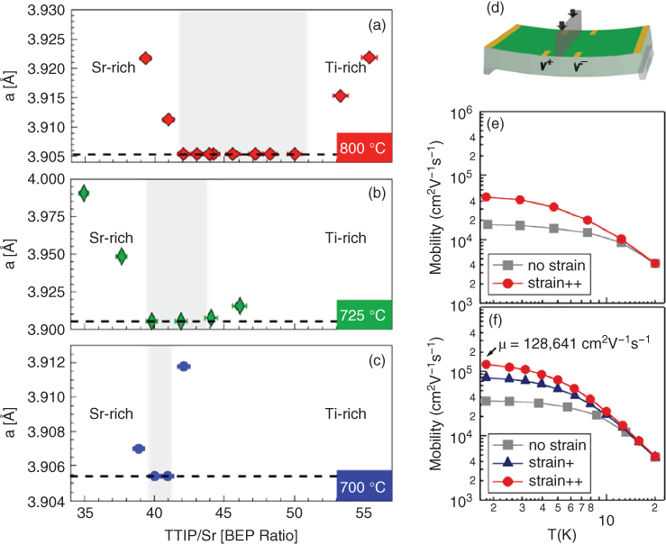
Figure 26.9 (a–c) Change in the out‐of‐plane lattice parameter of homoepitaxial SrTiO3 films grown by hybrid MBE at different growth temperatures – 800, 725, and 700 °C – showing a shrinking growth window with decreasing temperature. (d) Schematic of the three‐point bending setup that allows application of uniaxial strain to the thin film. (e, f) Effect of strain on mobility in La‐doped SrTiO3 films with carrier concentrations of 3.6 × 10¹⁷ and 7.5 × 1017 cm−3, respectively.
Point defects, either in the form of vacancies or interstitials, strongly affect the physical properties. Having an accessible growth window for SrTiO3 eliminates non‐stoichiometry due to fluctuations in the beam flux, thus minimizing defect concentrations in thin films. As a result, electron mobilities exceeding 50 000 cm2 V−1 s−1 (n = 8 × 1017 cm−3) have been achieved in La‐doped SrTiO3 films at 2 K [150]. This value is higher than those reported in the bulk single crystals (22 000 cm2 V−1 s−1) [151] by more than twice, and much higher than those reported for films grown by PLD (6600 cm2 V−1 s−1) [152] or any other techniques. This suggests that hybrid MBE provides excellent control over defects [18]. Electron mobility can be further enhanced by 300% under strain [Figure 26.9(d–f)] [147]. High mobilities at low temperature also allow for quantum effects such as Shubnikov–de Haas oscillations to be observable in magnetic fields, enabling direct measurement of electron effective mass [ 18,153]. Recently, the use of a hybrid MBE approach has led to the discovery of quantum Hall effects for the first time in perovskite oxides [154].
Similar growth windows have been shown to exist for vanadium precursor – vanadium‐oxy‐triisopropoxide (VTIP) – during the growth of SrVO3, LaVO3, and CaVO3 [155–158]. Both TTIP and VTIP precursors, having the same isopropoxide (C3H7O–) group bonded with the metal ion, are expected to show similar growth kinetics at the substrate surface. Oxygen‐containing precursor has now been successfully employed for zirconates (zirconium tert‐butoxide) as well ruthenates (ruthenium tetroxide) [159,160].
26.4.2.1 Challenges with Hybrid MBE
26.4.2.1.1 Carbon Contamination
As with any other approaches, hybrid MBE also has its limitations. Metal–organic precursors contain carbon, which can potentially result in contaminations within the film or at the film surface. Below 725 °C, carbon contaminations exceeding 2 × 1018 cm−3 have been detected in SrTiO3 films using dynamic secondary ion mass spectroscopy (SIMS). Carbon contamination was found to be negligible (<1 × 1017 cm−3) at higher substrate temperatures (≥800 °C), likely due to dissociation of the C–O bond in TTIP [161].
26.4.2.1.2 Volatility and By‐products
In conventional MBE, most of the source elements or species formed during reaction in the growth chamber have low vapor pressure. Therefore, they get permanently attached to the chamber walls. They desorb during high‐temperature bake out if their vapor pressure is sufficiently high. Meanwhile in hybrid MBE, precursors that stick to the cryo‐panel during growth also desorb during warm‐up due to their high vapor pressure, even at room temperature. As a result, the pressure inside the growth chamber may rise over time to as high as 1 × 10⁻⁴ Torr. This can put a tremendous load on the vacuum pumps if proper caution is not taken during regeneration [162]. At the same time, intercell contamination should also be considered due to the high volatility of these by‐products.
26.4.2.1.3 Availability of UHV Compatible Precursors
While precursors already bonded with oxygen is desirable, it may not be trivial to find such precursors for every element for which conventional MBE may be problematic. So, one must resort to the idea of using other available precursors. Several precursors exist for various elements and have been shown to work in atomic layer deposition (ALD) and/or chemical vapor deposition (CVD). However, they may not be compatible with the UHV MBE approach. Many of these precursors that have been successfully used for depositing metals and their oxides contain halogen atoms, or sulfur, or nitrogen, which can potentially react with residual water vapors in the chamber to form corrosive acids. Other considerations when choosing appropriate precursors include their vapor pressures, thermal decomposition temperatures, and reactivity with oxygen at growth temperatures.
26.4.3 Radical‐Based Molecular Beam Epitaxy
As stated earlier, the flexible perovskite crystal structure can accommodate a variety of elements at A and B‐sites. Since both the elements need to be oxidized, there is competition for the limited oxygen available during UHV growth. When the oxidation potential of the two elements is similar, both elements will be oxidized without preference. However, a serious problem can arise for MBE growers when they have very different affinities toward oxygen. Figure 26.10 shows the values of standard half‐cell oxidation potentials for some of the elements commonly present in perovskite oxides. The ones with higher oxidation potentials are easier to oxidize than those with lower oxidation potentials. For example, in the case of nickel, which has a low oxidation potential, it was shown that oxidation of nickel is challenging during MBE growth of PrNiO3 using conventional solid sources [164]. At oxygen pressure ∼1 × 10⁻⁶ Torr, binary oxides of Ni and Pr were stabilized. Nickel was present in a reduced +2 state in the form of NiO, instead of the desired +3 state. Even at higher oxygen pressures, Ni +2 was not eliminated.
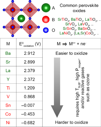
Figure 26.10 Half‐cell oxidation potentials for some of the elements commonly present in perovskite oxides. Note that n = 2 for Ba and Sr; n = 3 for La, Y, Ti, V, Co, and Ni; n = 4 for Sn.
Source: Reproduced with permission from Ref. [163].
Several routes have been proposed to circumvent this challenge, such as high substrate temperature, high oxygen pressure, and/or use of reactive gases like ozone [ 100, 164]. However, these approaches may not be feasible for all the elements with low oxidation potential. For example, in case of tin (Sn), at high substrate temperatures, the growth rate of SnO2 is dramatically reduced due to the formation and simultaneous desorption of highly volatile SnO [165]. The use of high oxygen pressure or ozone, on the other hand, can lead to flux instabilities if a conventional effusion cell is used. Alternatively, a hybrid MBE method can be employed as shown earlier for titanates and vanadates, which supplies metal–organic precursors already bonded with oxygen to maintain the stoichiometry and oxidation states. Although an oxygen‐containing precursor exists for many of these low‐oxidation‐potential metals, they may not be feasible for MBE growth. For example, in case of tin, tin tert‐butoxide (TTB) is an oxygen‐containing precursor but was found to have low vapor pressure and be thermally unstable for MBE growth of Sn‐based compounds [166,167].
Recently, Jalan's group at the University of Minnesota has shown that a novel radical‐based MBE approach can be exploited to increase the reactivity of the metal toward oxygen. The unique aspect of this approach is that it does not rely on improving the reactivity of oxidants but rather on making the metal itself more reactive by forming its radicals. This approach, demonstrated for Sn, used hexamethylditin (HMDT)–(CH3)3Sn–Sn(CH3)3 as the tin precursor. HMDT provides several advantages over a solid Sn source. First, it has a much higher vapor pressure than solid tin, which permits high and scalable growth rates. Second, the dissociation of the Sn–Sn bond with lower bond energy than the Sn–C bond results in the formation of (CH3)3Sn• radicals that have higher reactivity than metallic Sn. Better reactivity of these radicals helps in maintaining the correct oxidation state (+4) of Sn, even in low oxygen pressures. The formation of highly reactive radicals also allows for this approach to work with the less reactive molecular oxygen for the growth of binary and ternary tin oxides such as SnO2 and BaSnO3, respectively [ 163,168]. Use of HMDT also allows oxygen stoichiometry to be maintained [169].
The high volatility of HMDT precursor also facilitated a growth window during MBE of BaSnO3 films, allowing for highly reproducible film structures. Figure 26.11 shows the variation of out‐of‐plane lattice parameter and cation ratio measured using RBS as a function of cation flux ratios. There was a range of Sn:Ba ratio for which cation stoichiometry was maintained as 1:1, suggesting a self‐regulated growth regime. Within the growth window, nominally same thickness of the films is indicative of adsorption‐controlled growth mode [142]. Unexpectedly, lattice parameters for Ba‐deficient (or Sn‐rich) films were the same as stoichiometric films, irrespective of the flux ratio. It was hypothesized that the presence of anti‐site defects, where Ba sites are occupied by excess Sn, likely in the +2 state, may cause this unusual trend [142].
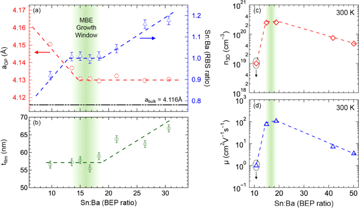
Figure 26.11 Variation of (a) out‐of‐plane lattice parameter and cation ratio as measured by Rutherford backscattering spectrometry and (b) thickness of BaSnO3 films grown by radical MBE approach as a function of Sn:Ba beam equivalent pressure ratio. The green shaded region shows the range of Sn:Ba ratio in which cation stoichiometry was maintained as 1:1 in a self‐regulatory manner. In this region, thickness was nominally constant, suggesting an absorption‐controlled growth mode. (c) and (d) show the variation in carrier density and mobility, respectively, as a function of cation flux ratio.
Source: Reproduced from Ref. [142] with permission from the Royal Society of Chemistry.
Non‐stoichiometry‐related defects (vacancies, interstitials, anti‐site defects, etc.) are found to have a strong influence on the electronic properties of La‐doped stannates (BaSnO3 and SrSnO3) [ 7, 9, 142]. These defects neutralize some of the charge carriers, resulting in a smaller carrier density and increased scattering, thus leading to lower carrier mobility as shown in Figure 26.11 [ 7, 9,170]. For example, compensation due to point defects can be visualized in terms of a simple defect reaction [142].
Ba‐deficient conditions:
Overall defect reaction:
Sn‐deficient conditions:
Overall defect reaction:
Having an assessible growth window using the radical‐MBE approach helps in minimizing defects in BaSnO3. This has led to the highest reported conductivity, to date, in BaSnO3 (>104 S cm−1) amongst all semiconducting perovskite oxides at room temperature [7]. This method has now been extended to SrSnO3. The highest reported mobility in La‐doped SrSnO3 was achieved with this approach [9]. Although growth of BaSnO3 has not been possible so far with the conventional MBE approach, use of SnO2 instead of metallic Sn as a source for tin has been successful in producing films with good structural quality and high mobility [8,171]. However, growth of conductive SrSnO3 film using SnO2 remains elusive [16].
26.5 Outlook
Given the important role of III–V MBE in developing new device applications, it is reasonable to discuss the important current (and potential) role of oxide MBE in bringing oxide electronics a step closer to reality. To put our discussion in context, we show a timeline in Figure 26.12(a) indicating how mobility of the GaAs/AlGaAs system (as a measure of materials quality) has improved over the years. For instance, the extreme level of atomic layer control with improved defect concentrations afforded by III–V MBE led to the discovery of the fractional quantum Hall effect in AlGaAs/GaAs heterostructures, which later went on to receive a Nobel Prize in Physics in the year 1998 [172–174]. Spanning almost four decades since the first report of modulation doping in AlGaAs/GaAs heterostructures [175], the highest low‐temperature mobility in this system has increased more than four orders of magnitude during this time. While much effort was initially directed toward optimizing the structure in order to enhance mobility [ 175–182], the major increment in the mobility values came only with improvements in the level of purity achievable inside the growth chamber [183–193]. III–V MBE with better vacuum and ultra‐high‐purity sources played a key role in this process.
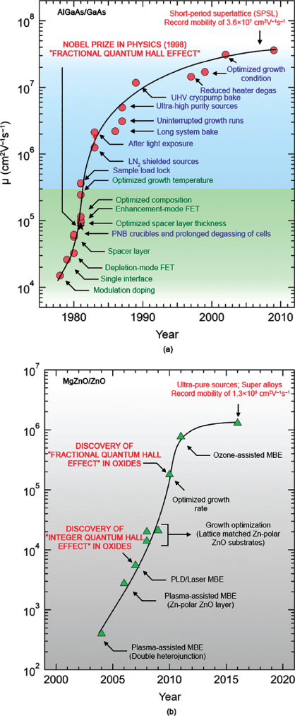
Figure 26.12 Timeline of highest reported low‐temperature mobility in two‐dimensional electron gas systems at the interface of (a) conventional semiconductors (AlGaAs/GaAs) and (b) binary semiconducting oxides (MgZnO/ZnO).
Taking analogy from III–V MBE, a similar trend has been observed for Mg(Mn)ZnO/ZnO heterostructures [Figure 26.12(b)]. Modifications to the growth chamber and amendments to the film structure have resulted in an almost four orders of magnitude increase in low‐temperature mobility [ 42, 115194–200]. Enhanced mobility has also guided the discovery of novel quantum phenomena never seen in oxide systems. Importantly, this remarkable growth has been achieved in less than two decades [201]. Similarly, in perovskite oxides such as doped SrTiO3 (see Figure 26.13), in just over a decade, a significant improvement in low‐temperature mobility, by over three orders of magnitude, has been observed [ 18, 147, 152, 154202–205].

Figure 26.13 Evolution of low‐temperature mobility in doped SrTiO3 thin films.
The aforementioned high mobility value in SrTiO3 is at 2 K, which has led to the discovery of new physics and also validated theoretical models that otherwise could not have been validated without these high‐quality materials. It is noteworthy that oxide MBE including the development of a novel hybrid MBE has played a significant role in this impressive achievement. However, at room temperature, SrTiO3 possesses mobility <10 cm2 Vs−1, which on the other hand has limited their use in electronics operated at room temperature.
Only recently, the discovery of high mobility at room temperature in doped‐BaSnO3 has projected perovskite oxides for the first time onto an equal footing with conventional semiconductors for applications in oxide electronics. In addition, BaSnO3 is also a wide‐bandgap material [169], making it optically transparent [206] and relevant for power electronic applications. For instance, the room‐temperature conductivity in BaSnO3 has already attained values comparable to commercially available transparent conductors (Figure 26.14).

Figure 26.14 Mobility (μ) vs. carrier density (n) relationship for various binary transparent conductors along with La‐doped BaSnO3 films. Data point for Nb‐doped SrTiO3 is also shown for comparison. The shaded region is the generally accepted industry standard for transparent conductors.
The question that remains to be answered, however, is: can the mobilities of stannate films be further improved? One of the main challenges with the thin‐film BaSnO3 films is the unavailability of lattice‐matched substrates. Due to large lattice mismatch between the substrate and BaSnO3 (Figure 26.15), films relax within a nanometer thickness via formation of misfit dislocations [163]. In addition to these misfit dislocations at the interface, threading dislocations also exist, which can propagate through the entire film thickness.

Figure 26.15 Lattice parameter of various commercially available substrates in comparison with BaSnO3. Lattice parameter of SrSnO3 is also shown on the plot as the material can be grown in situ as a template layer.
Prior reports have argued that dislocation cores can be comprised of Ba vacancies which can also compensate for charge carriers similar to non‐stoichiometric defects [7]. Inspection of individual electron‐scattering mechanisms using first‐principle calculations also revealed that at low carrier concentrations, dislocation scattering is the primary mobility‐limiting scattering mechanism. At higher concentrations, mobility is mostly limited by ionized impurity scattering and/or phonon scattering [ 7,212]. Therefore, efforts need to be made to minimize the effect of dislocations on electronic properties. Once the issue of lattice mismatch is addressed, attention should move toward developing modulation‐doped structures in addition to improving the vacuum and purity level in the MBE growth chamber.
26.6 Summary
Oxide MBE has come a long way since its introduction in the late 1970s. Significant progress in the growth and controlled doping (both extrinsic and intrinsic) of oxide semiconductors has been made. For example, low‐temperature electron mobility in SrTiO3 or ZnO‐based heterostructures has improved by several orders of magnitude over the last decade, owing to the advancements made in the design of the MBE chamber, choice of materials for vacuum components, vacuum level, purity of sources, and modifications made to growth processes as well. The major bottleneck still exists in preparing device‐quality films of stannate compounds suitable for room‐temperature electronic applications. To date, the known limiting factor is largely substrate‐induced defects. Intrinsic defects, extrinsic impurities, and reproducibility are expected to play an important role in realizing the full potential of stannate compounds, once the issues related to substrate‐induced defects are addressed. In this context, it is perhaps reasonable to say that oxide MBE has yet to reach its pinnacle for oxide electronics operating at room temperature.
Acknowledgments
We acknowledge support from the Air Force Office of Scientific Research (AFOSR) through Grant FA9550‐16‐1‐0205, the National Science Foundation through award numbers DMR‐1410888, DMR‐1607318, and DMR‐1741801, the UMN MRSEC program under award number DMR‐1420013, the DOE Center for Quantum Materials (CQM) under DE‐SC0016371, and the RDF Fund of the Institute on the Environment (UMN). A. P. would like to acknowledge support from a UMN Doctoral Dissertation Fellowship. The authors would also like to thank Steve May for careful reading of the manuscript.
References
- 1 Green, M.L., Gusev, E.P., Degraeve, R., and Garfunkel, E.L. (2001). J. Appl. Phys. 90 (5): 2057–2121.
- 2 Ohta, H., Orita, M., Hirano, M. et al. (2000). Appl. Phys. Lett. 76 (19): 2740–2742.
- 3 Pearton, S.J., Yang, J., Cary, P.H. et al. (2018). Appl. Phys. Rev. 5 (1): 011301.
- 4 Wong, M.H., Sasaki, K., Kuramata, A. et al. (2016). IEEE Electr. Device L. 37 (2): 212–215.
- 5 Roberts, S. (1947). Phys. Rev. 71 (12): 890–895.
- 6 Jaffe, H. (2006). J. Am. Ceram. Soc. 41 (11): 494–498.
- 7 Prakash, A., Xu, P., Faghaninia, A. et al. (2017). Nat. Commun. 8: 15167.
- 8 Paik, H., Chen, Z., Lochocki, E. et al. (2017). APL Mater. 5 (11): 116107.
- 9 Wang, T., Thoutam, L.R., Prakash, A. et al. (2017). Phys. Rev. Materials 1 (6): 061601.
- 10 Goldschmidt, V.M. (1926). Naturwissenschaften 14 (21): 477–485.
- 11 Peña, M.A. and Fierro, J.L.G. (2001). Chem. Rev. 101 (7): 1981–2018.
- 12 Mats, J. and Peter, L. (2008). J. Phys. Condens. Matter 20 (26): 264001.
- 13 Engel‐Herbert, R. (2013). Molecular Beam Epitaxy, 417–449. Oxford: Elsevier.
- 14 Glazer, A. (1975). Acta Crystallogr. Sect. A 31 (6): 756–762.
- 15 Wang, T., Pitike, K.C., Yuan, Y. et al. (2016). APL Mater. 4 (12): 126111.
- 16 Schumann, T., Raghavan, S., Ahadi, K. et al. (2016). J. Vac. Sci. Technol. A 34 (5): 050601.
- 17 Higuchi, T., Tsukamoto, T., Sata, N. et al. (1998). Phys. Rev. B 57 (12): 6978–6983.
- 18 Son, J., Moetakef, P., Jalan, B. et al. (2010). Nat. Mater. 9: 482.
- 19 Spinelli, A., Torija, M.A., Liu, C. et al. (2010). Phys. Rev. B 81 (15): 155110.
- 20 Iglesias, L., Sarantopoulos, A., Magén, C., and Rivadulla, F. (2017). Phys. Rev. B 95 (16): 165138.
- 21 Ganguly, K., Prakash, A., Jalan, B., and Leighton, C. (2017). APL Mater. 5 (5): 056102.
- 22 Lee, W.J., Kim Hyung, J., Sohn, E. et al. (2015). Phys. Status Solidi A 212 (7): 1487–1493.
- 23 Paladino, A.E., Rubin, L.G., and Waugh, J.S. (1965). J. Phys. Chem. Solids 26 (2): 391–397.
- 24 De Souza, R.A., Metlenko, V., Park, D., and Weirich, T.E. (2012). Phys. Rev. B 85 (17): 174109.
- 25 May, S.J., Kim, J.W., Rondinelli, J.M. et al. (2010). Phys. Rev. B 82 (1): 014110.
- 26 Haeni, J.H., Irvin, P., Chang, W. et al. (2004). Nature 430: 758.
- 27 Bednorz, J.G. and Müller, K.A. (1986). Z. Phys. B: Condens. Matter 64 (2): 189–193.
- 28 Coey, J.M.D., Viret, M., Ranno, L., and Ounadjela, K. (1995). Phys. Rev. Lett. 75 (21): 3910–3913.
- 29 Moreira dos Santos, A., Parashar, S., Raju, A.R. et al. (2002). Solid State Commun. 122 (1): 49–52.
- 30 Wang, J., Neaton, J.B., Zheng, H. et al. (2003). Science 299 (5613): 1719.
- 31 Jin, S., Tiefel, T.H., McCormack, M. et al. (1994). Science 264 (5157): 413.
- 32 Ohtomo, A. and Hwang, H.Y. (2004). Nature 427: 423.
- 33 Reyren, N., Thiel, S., Caviglia, A.D. et al. (2007). Science 317 (5842): 1196.
- 34 Gozar, A., Logvenov, G., Kourkoutis, L.F. et al. (2008). Nature 455: 782.
- 35 Smadici, S., Lee, J.C.T., Wang, S. et al. (2009). Phys. Rev. Lett. 102 (10): 107004.
- 36 Takahashi, K.S., Kawasaki, M., and Tokura, Y. (2001). Appl. Phys. Lett. 79 (9): 1324–1326.
- 37 Chakhalian, J., Freeland, J.W., Srajer, G. et al. (2006). Nat. Phys. 2: 244.
- 38 Brinkman, A., Huijben, M., van Zalk, M. et al. (2007). Nat. Mater. 6: 493.
- 39 Moetakef, P., Williams, J.R., Ouellette, D.G. et al. (2012). Phys. Rev. X 2 (2): 021014.
- 40 Lee, J.S., Xie, Y.W., Sato, H.K. et al. (2013). Nat. Mater. 12: 703.
- 41 Ayino, Y., Xu, P., Tigre‐Lazo, J. et al. (2018). Phys. Rev. Materials 2 (3): 031401.
- 42 Tsukazaki, A., Ohtomo, A., Kita, T. et al. (2007). Science 315 (5817): 1388.
- 43 Trier, F., Prawiroatmodjo, G.E.D.K., Zhong, Z. et al. (2016). Phys. Rev. Lett. 117 (9): 096804.
- 44 Bousquet, E., Dawber, M., Stucki, N. et al. (2008). Nature 452: 732.
- 45 Xu, P., Droubay, T.C., Jeong, J.S. et al. (2015). Adv. Mater. Interfaces 3 (2): 1500432.
- 46 Dikin, D.A., Mehta, M., Bark, C.W. et al. (2011). Phys. Rev. Lett. 107 (5): 056802.
- 47 Cen, C., Thiel, S., Hammerl, G. et al. (2008). Nat. Mater. 7: 298.
- 48 Bell, C., Harashima, S., Kozuka, Y. et al. (2009). Phys. Rev. Lett. 103 (22): 226802.
- 49 Caviglia, A.D., Gabay, M., Gariglio, S. et al. (2010). Phys. Rev. Lett. 104 (12): 126803.
- 50 Ben Shalom, M., Ron, A., Palevski, A., and Dagan, Y. (2010). Phys. Rev. Lett. 105 (20): 206401.
- 51 Bark, C.W., Felker, D.A., Wang, Y. et al. (2011). Proc. Natl. Acad. Sci. U.S.A. 108 (12): 4720.
- 52 Santander‐Syro, A.F., Fortuna, F., Bareille, C. et al. (2014). Nat. Mater. 13: 1085.
- 53 Ohtomo, A., Muller, D.A., Grazul, J.L., and Hwang, H.Y. (2002). Nature 419: 378.
- 54 Smadici, Ş., Abbamonte, P., Bhattacharya, A. et al. (2007). Phys. Rev. Lett. 99 (19): 196404.
- 55 Chaloupka, J. and Khaliullin, G. (2008). Phys. Rev. Lett. 100 (1): 016404.
- 56 Okamoto, S. and Maier, T.A. (2008). Phys. Rev. Lett. 101 (15): 156401.
- 57 Bhattacharya, A., May, S.J., te Velthuis, S.G.E. et al. (2008). Phys. Rev. Lett. 100 (25): 257203.
- 58 Lee, H., Campbell, N., Lee, J. et al. (2018). Nat. Mater. 17 (3): 231–236.
- 59 Matzdorf, R., Fang, Z., Ismail et al. (2000). Science 289 (5480): 746.
- 60 Hwang, H.Y., Iwasa, Y., Kawasaki, M. et al. (2012). Nat. Mater. 11: 103.
- 61 Mundy, J.A., Brooks, C.M., Holtz, M.E. et al. (2016). Nature 537: 523.
- 62 Chambers, S.A., Engelhard, M.H., Shutthanandan, V. et al. (2010). Surf. Sci. Rep. 65 (10): 317–352.
- 63 Lee, D., Lu, H., Gu, Y. et al. (2015). Science 349 (6254): 1314.
- 64 Nakagawa, N., Hwang, H.Y., and Muller, D.A. (2006). Nat. Mater. 5: 204.
- 65 Breckenfeld, E., Bronn, N., Karthik, J. et al. (2013). Phys. Rev. Lett. 110 (19): 196804.
- 66 Dildar, I.M., Boltje, D.B., Hesselberth, M.H.S. et al. (2013). Appl. Phys. Lett. 102 (12): 121601.
- 67 Xu, P., Ayino, Y., Cheng, C. et al. (2016). Phys. Rev. Lett. 117 (10): 106803.
- 68 Sato, H.K., Bell, C., Hikita, Y., and Hwang, H.Y. (2013). Appl. Phys. Lett. 102 (25): 251602.
- 69 Warusawithana, M.P., Richter, C., Mundy, J.A. et al. (2013). Nat. Commun. 4: 2351.
- 70 Mannhart, J. and Schlom, D.G. (2010). Science 327 (5973): 1607.
- 71 Byung Du, A., Hye‐Ji, J., Jiazhen, S. et al. (2015). Semicond. Sci. Technol. 30 (6): 064001.
- 72 Parsons, R. (1991). Thin Film Processes II, 177. New York: Academic Press.
- 73 Christen, H.M. and Eres, G. (2008). J. Phys. Condens. Matter 20 (26): 264005.
- 74 Eason, R. (2007). Pulsed Laser Deposition of Thin Films: Applications‐Led Growth of Functional Materials. New York: Wiley.
- 75 Ohnishi, T., Shibuya, K., Yamamoto, T., and Lippmaa, M. (2008). J. Appl. Phys. 103 (10): 103703.
- 76 Poppe, U., Schubert, J., Arons, R.R. et al. (1988). Solid State Commun. 66 (6): 661–665.
- 77 Torija Maria, A., Sharma, M., Gazquez, J. et al. (2011). Adv. Mater. 23 (24): 2711–2715.
- 78 Ganguly, K., Ambwani, P., Xu, P. et al. (2015). APL Mater. 3 (6): 062509.
- 79 Li, Y. and Tanabe, K. (1998). J. Appl. Phys. 83 (12): 7744–7752.
- 80 Ambwani, P., Xu, P., Haugstad, G. et al. (2016). J. Appl. Phys. 120 (5): 055704.
- 81 Le, Y. and Tanabe, K. (1999). IEEE T. Appl. Supercon. 9 (2): 1586–1589.
- 82 Arthur, J.R. (1968). J. Appl. Phys. 39 (8): 4032–4034.
- 83 Cho, A.Y. and Arthur, J.R. (1975). Prog. Solid State Chem. 10: 157–191.
- 84 McCray, W.P. (2007). Nat. Nanotechnol. 2: 259.
- 85 D. G. Schlom, https://www.slideshare.net/nirupam12/d-schlom-oxide-molecularbeam-epitaxy (2012).
- 86 S. J. May, Materials Research Society: Tutorial on Discovery of Functional Oxides by Computational and Epitaxial Design (2016).
- 87 Hirose, M., Fischer, A., and Ploog, K. (1978). Phys. Status Solidi A 45: K175.
- 88 Ploog, K., Fischer, A., Trommer, R., and Hirose, M. (1979). J. Vac. Sci. Technol. 16 (2): 290–294.
- 89 Stall, R.A. (1983). J. Vac. Sci. Technol. B 1 (2): 135–137.
- 90 Betts, R.A. and Pitt, C.W. (1985). Electron. Lett. 21 (21): 960–962.
- 91 Chu, C.W., Hor, P.H., Meng, R.L. et al. (1987). Phys. Rev. Lett. 58 (4): 405–407.
- 92 Cava, R.J., Batlogg, B., van Dover, R.B. et al. (1987). Phys. Rev. Lett. 58 (16): 1676–1679.
- 93 Wu, M.K., Ashburn, J.R., Torng, C.J. et al. (1987). Phys. Rev. Lett. 58 (9): 908–910.
- 94 Qi‐rui, Z., Lie‐zhao, C., Yi‐tai, Q. et al. (1987). Solid State Commun. 63 (6): 535–536.
- 95 Hazen, R.M., Prewitt, C.T., Angel, R.J. et al. (1988). Phys. Rev. Lett. 60 (12): 1174–1177.
- 96 Bednorz, J.G. and Müller, K.A. (1988). Rev. Mod. Phys. 60 (3): 585–600.
- 97 Webb, C., Weng, S.L., Eckstein, J.N. et al. (1987). Appl. Phys. Lett. 51 (15): 1191–1193.
- 98 Schlom, D.G., Eckstein, J.N., Hellman, E.S. et al. (1988). Appl. Phys. Lett. 53 (17): 1660–1662.
- 99 Eckstein, J.N., Schlom, D.G., Hellman, E.S. et al. (1989). J. Vac. Sci. Technol. B 7 (2): 319–323.
- 100 Berkley, D.D., Johnson, B.R., Anand, N. et al. (1988). Appl. Phys. Lett. 53 (20): 1973–1975.
- 101 Berkley, D.D., Goldman, A.M., Johnson, B.R. et al. (1989). Rev. Sci. Instrum. 60 (12): 3769–3774.
- 102 Kearns, D.M., Gillen, D.R., Voulot, D. et al. (2001). J. Vac. Sci. Technol. A 19 (3): 993–997.
- 103 Chambers, S.A. (2000). Surf. Sci. Rep. 39 (5): 105–180.
- 104 Chambers, S.A., Wang, C.M., Thevuthasan, S. et al. (2002). Thin Solid Films 418 (2): 197–210.
- 105 Baiutti, F., Wrobel, F., Christiani, G., and Logvenov, G. (2018). Metal Oxide‐Based Thin Film Structures, 53–78. Amsterdam: Elsevier.
- 106 D. G. Schlom, Thesis, Stanford University, 1990.
- 107 Farrow, R.F.C. (1995). Molecular Beam Epitaxy: Applications to Key Materials. Amsterdam: Elsevier.
- 108 Shunji, W., Maki, K., and Takashi, H. (1990). Jpn. J. Appl. Phys. 29 (7A): L1111.
- 109 Nonaka, H., Shimizu, T., Hosokawa, S. et al. (1992). Surf. Interface Anal. 19 (1–12): 353–357.
- 110 Voogt, F.C., Hibma, T., Zhang, G.L. et al. (1995). Surf. Sci. 331–333: 1508–1514.
- 111 Fujii, T., Alders, D., Voogt, F.C. et al. (1996). Surf. Sci. 366 (3): 579–586.
- 112 Voogt, F.C., Smulders, P.J.M., Wijnja, G.H. et al. (2001). Phys. Rev. B 63 (12): 125409.
- 113 Izyumskaya, N., Avrutin, V., Schoch, W. et al. (2004). J. Cryst. Growth 269 (2): 356–361.
- 114 McConnell, R.D. and Noufi, R. (2012). Science and Technology of Thin Film Superconductors 2. Berlin: Springer.
- 115 Falson, J., Kozuka, Y., Uchida, M. et al. (2016). Sci. Rep. 6: 26598.
- 116 Hellman, E.S. and Hartford, E.H. (1994). J. Vac. Sci. Technol. B 12 (2): 1178–1180.
- 117 Theis, C.D. and Schlom, D.G. (1996). J. Vac. Sci. Technol. A 14 (4): 2677–2679.
- 118 Kim, Y.S., Bansal, N., Chaparro, C. et al. (2010). J. Vac. Sci. Technol. A 28 (2): 271–276.
- 119 Sakai, S., Oohira, T., Kasai, Y. et al. (1996). Proc. SPIE 2697: 217–227.
- 120 Chai, J., Mendelsberg, R.J., Reeves, R.J. et al. (2010). J. Electron. Mater. 39 (5): 577–583.
- 121 Kim, Y.‐S., Bansal, N., and Oh, S. (2011). J. Vac. Sci. Technol. A 29 (4): 041505.
- 122 Kim, Y.‐S., Bansal, N., and Oh, S. (2010). J. Vac. Sci. Technol. A 28 (4): 600–602.
- 123 Klausmeier‐Brown, M.E., Eckstein, J.N., Bozovic, I., and Virshup, G.F. (1992). Appl. Phys. Lett. 60 (5): 657–659.
- 124 Ichimiya, A. and Cohen, P.I. (2004). Reflection High‐Energy Electron Diffraction. Cambridge: Cambridge University Press.
- 125 Haeni, J.H., Theis, C.D., and Schlom, D.G. (2000). J. Electroceram. 4 (2): 385–391.
- 126 Haislmaier, R.C., Stone, G., Alem, N., and Engel‐Herbert, R. (2016). Appl. Phys. Lett. 109 (4): 043102.
- 127 Günther, K. (1958). Z. Naturforschg. 13: 1081–1089.
- 128 Theis, C.D. and Schlom, D.G. (1997). J. Cryst. Growth 174 (1): 473–479.
- 129 Theis, C.D., Yeh, J., Schlom, D.G. et al. (1998). Thin Solid Films 325 (1): 107–114.
- 130 Barin, I. (1995). Thermochemical Data of Pure Substances. Weinheim: VCH.
- 131 Lamoreaux, R.H., Hildenbrand, D.L., and Brewer, L. (1987). J. Phys. Chem. Rev. Data 16 (3): 419–443.
- 132 Migita, S., Kasai, Y., Ota, H., and Sakai, S. (1997). Appl. Phys. Lett. 71 (25): 3712–3714.
- 133 Theis, C.D., Yeh, J., Schlom, D.G. et al. (1998). Appl. Phys. Lett. 72 (22): 2817–2819.
- 134 Ihlefeld, J.F., Kumar, A., Gopalan, V. et al. (2007). Appl. Phys. Lett. 91 (7): 071922.
- 135 Lee, J.H., Ke, X., Misra, R. et al. (2010). Appl. Phys. Lett. 96 (26): 262905.
- 136 Brooks, C.M., Misra, R., Mundy, J.A. et al. (2012). Appl. Phys. Lett. 101 (13): 132907.
- 137 Jalan, B., Moetakef, P., and Stemmer, S. (2009). Appl. Phys. Lett. 95 (3): 032906.
- 138 Endo, K., Mariyasu, Y., Misawa, S., and Yoshida, S. (1991). Physica C 185–189: 1995–1996.
- 139 Endo, K., Saya, S., Misawa, S., and Yoshida, S. (1991). Thin Solid Films 206 (1): 143–145.
- 140 Jalan, B., Engel‐Herbert, R., Cagnon, J., and Stemmer, S. (2009). J. Vac. Sci. Technol. A 27 (2): 230–233.
- 141 Jalan, B., Engel‐Herbert, R., Wright, N.J., and Stemmer, S. (2009). J. Vac. Sci. Technol. A 27 (3): 461–464.
- 142 Prakash, A., Xu, P., Wu, X. et al. (2017). J. Mater. Chem. C 5 (23): 5730–5736.
- 143 Kanai, H.K.T. and Inoue, H. (1985). Kagaku Kogaku Ronbun. 11: 317.
- 144 Fictorie, C.P., Evans, J.F., and Gladfelter, W.L. (1994). J. Vac. Sci. Technol. A 12 (4): 1108–1113.
- 145 Roth, J., Arriaga, E., Brahlek, M. et al. (2017). J. Vac. Sci. Technol. A 36 (2): 020601.
- 146 Yuya, M., Kei, S.T., Yoshinori, T., and Masashi, K. (2014). Appl. Phys. Express 7 (12): 125502.
- 147 Jalan, B., Allen, S.J., Beltz, G.E. et al. (2011). Appl. Phys. Lett. 98 (13): 132102.
- 148 Ahn, K.‐H., Park, Y.‐B., and Park, D.‐W. (2003). Surf. Coat. Technol. 171 (1): 198–204.
- 149 Taylor, C.J., Gilmer, D.C., Colombo, D.G. et al. (1999). J. Am. Ceram. Soc. 121 (22): 5220–5229.
- 150 Cain, T.A., Kajdos, A.P., and Stemmer, S. (2013). Appl. Phys. Lett. 102 (18): 182101.
- 151 Tufte, O.N. and Chapman, P.W. (1967). Phys. Rev. 155 (3): 796–802.
- 152 Kozuka, Y., Hikita, Y., Bell, C., and Hwang, H.Y. (2010). Appl. Phys. Lett. 97 (1): 012107.
- 153 Jalan, B., Stemmer, S., Mack, S., and Allen, S.J. (2010). Phys. Rev. B 82 (8): 081103.
- 154 Matsubara, Y., Takahashi, K.S., Bahramy, M.S. et al. (2016). Nat. Commun. 7: 11631.
- 155 Zhang, H.‐T., Dedon, L.R., Martin, L.W., and Engel‐Herbert, R. (2015). Appl. Phys. Lett. 106 (23): 233102.
- 156 Brahlek, M., Zhang, L., Eaton, C. et al. (2015). Appl. Phys. Lett. 107 (14): 143108.
- 157 Brahlek, M., Zhang, L., Zhang, H.‐T. et al. (2016). Appl. Phys. Lett. 109 (10): 101903.
- 158 Eaton, C., Lapano, J., Zhang, L. et al. (2017). J. Vac. Sci. Technol. A 35 (6): 061510.
- 159 Kajdos, A.P., Ouellette, D.G., Cain, T.A., and Stemmer, S. (2013). Appl. Phys. Lett. 103 (8): 082120.
- 160 Marshall, P.B., Kim, H., Ahadi, K., and Stemmer, S. (2017). APL Mater. 5 (9): 096101.
- 161 Jalan, B., Cagnon, J., Mates, T.E., and Stemmer, S. (2009). J. Vac. Sci. Technol. A 27 (6): 1365–1368.
- 162 Brahlek, M., Gupta, A.S., Lapano, J. et al. (2017). Adv. Funct. Mater. 28 (9): 1702772.
- 163 Prakash, A., Dewey, J., Yun, H. et al. (2015). J. Vac. Sci. Technol. A 33 (6): 060608.
- 164 Feigl, L., Schultz, B.D., Ohya, S. et al. (2013). J. Cryst. Growth 366: 51–54.
- 165 White, M.E., Tsai, M.Y., Wu, F., and Speck, J.S. (2008). J. Vac. Sci. Technol. A 26 (5): 1300–1307.
- 166 Wang, T., Prakash, A., Warner, E. et al. (2015). J. Vac. Sci. Technol. A 33 (2): 020606.
- 167 T. Wang, A. Prakash and B. Jalan, Private communication.
- 168 A. Prakash, T. Wang, R. Harkins, C. Cramer, W. L. Galdfelter and B. Jalan, In preparation.
- 169 Chambers, S.A., Kaspar, T.C., Prakash, A. et al. (2016). Appl. Phys. Lett. 108 (15): 152104.
- 170 Weston, L., Bjaalie, L., Krishnaswamy, K., and Van de Walle, C.G. (2018). Phys. Rev. B 97 (5): 054112.
- 171 Raghavan, S., Schumann, T., Kim, H. et al. (2016). APL Mater. 4 (1): 016106.
- 172 Laughlin, R.B. (1999). Rev. Mod. Phys. 71 (4): 863–874.
- 173 Stormer, H.L. (1999). Rev. Mod. Phys. 71 (4): 875–889.
- 174 Tsui, D.C. (1999). Rev. Mod. Phys. 71 (4): 891–895.
- 175 Dingle, R., Störmer, H.L., Gossard, A.C., and Wiegmann, W. (1978). Appl. Phys. Lett. 33 (7): 665–667.
- 176 Tsui, D.C. and Logan, R.A. (1979). Appl. Phys. Lett. 35 (2): 99–101.
- 177 Takashi, M., Satoshi, H., Toshio, F., and Kazuo, N. (1980). Jpn. J. Appl. Phys. 19 (5): L225.
- 178 Witkowski, L.C., Drummond, T.J., Stanchak, C.M., and Morkoç, H. (1980). Appl. Phys. Lett. 37 (11): 1033–1035.
- 179 Störmer, H.L., Pinczuk, A., Gossard, A.C., and Wiegmann, W. (1981). Appl. Phys. Lett. 38 (9): 691–693.
- 180 Witkowski, L.C., Drummond, T.J., Barnett, S.A. et al. (1981). Electron. Lett. 17: 126–128.
- 181 Drummond, T.J., Morkoç, H., Hess, K., and Cho, A.Y. (1981). J. Appl. Phys. 52 (8): 5231–5234.
- 182 Satoshi, H., Takashi, M., Toshio, F. et al. (1981). Jpn. J. Appl. Phys. 20 (4): L245.
- 183 Hiyamizu, S., Mimura, T., Fujii, T., and Nanb, K. (1980). Appl. Phys. Lett. 37 (9): 805–807.
- 184 Satoshi, H., Toshio, F., Takashi, M. et al. (1981). Jpn. J. Appl. Phys. 20 (6): L455.
- 185 Satoshi, H., Junji, S., Kazuo, N., and Tomonori, I. (1983). Jpn. J. Appl. Phys. 22 (10A): L609.
- 186 Foxon, C.T., Harris, J.J., Wheeler, R.G., and Lacklison, D.E. (1986). J. Vac. Sci. Technol. B 4 (2): 511–514.
- 187 Harris, J.J., Foxon, C.T., Barnham, K.W.J. et al. (1987). J. Appl. Phys. 61 (3): 1219–1221.
- 188 English, J.H., Gossard, A.C., Störmer, H.L., and Baldwin, K.W. (1987). Appl. Phys. Lett. 50 (25): 1826–1828.
- 189 Pfeiffer, L., West, K.W., Stormer, H.L., and Baldwin, K.W. (1989). Appl. Phys. Lett. 55 (18): 1888–1890.
- 190 Umansky, V., de‐Picciotto, R., and Heiblum, M. (1997). Appl. Phys. Lett. 71 (5): 683–685.
- 191 Pan, W., Xia, J.S., Shvarts, V. et al. (1999). Phys. Rev. Lett. 83 (17): 3530–3533.
- 192 Eisenstein, J.P., Cooper, K.B., Pfeiffer, L.N., and West, K.W. (2002). Phys. Rev. Lett. 88 (7): 076801.
- 193 Umansky, V., Heiblum, M., Levinson, Y. et al. (2009). J. Cryst. Growth 311 (7): 1658–1661.
- 194 Kazuto, K., Kenji, H., Ippei, N. et al. (2004). Jpn. J. Appl. Phys. 43 (10B): L1372.
- 195 Tampo, H., Shibata, H., Matsubara, K. et al. (2006). Appl. Phys. Lett. 89 (13): 132113.
- 196 Atsushi, T., Hiroyuki, Y., Shunsuke, A. et al. (2008). Appl. Phys. Express 1 (5): 055004.
- 197 Tsukazaki, A., Ohtomo, A., Kawasaki, M. et al. (2008). Phys. Rev. B 78 (23): 233308.
- 198 Nakano, M., Tsukazaki, A., Ohtomo, A. et al. (2010). Adv. Mater. 22 (8): 876–879.
- 199 Tsukazaki, A., Akasaka, S., Nakahara, K. et al. (2010). Nat. Mater. 9: 889.
- 200 Joseph, F., Denis, M., Yusuke, K. et al. (2011). Appl. Phys. Express 4 (9): 091101.
- 201 Joseph, F. and Masashi, K. (2018). Rep. Prog. Phys. 81 (5): 056501.
- 202 Olaya, D., Pan, F., Rogers, C.T., and Price, J.C. (2002). Appl. Phys. Lett. 80 (16): 2928–2930.
- 203 Takahashi, K.S., Matthey, D., Jaccard, D. et al. (2004). Appl. Phys. Lett. 84 (10): 1722–1724.
- 204 Cain, T.A., Moetakef, P., Jackson, C.A., and Stemmer, S. (2012). Appl. Phys. Lett. 101 (11): 111604.
- 205 Kobayashi, S., Mizumukai, Y., Ohnishi, T. et al. (2015). ACS Nano 9 (11): 10769–10777.
- 206 Arezoomandan, S., Prakash, A., Chanana, A. et al. (2018). Sci. Rep. 8 (1): 3577.
- 207 Rakhshani, A.E., Makdisi, Y., and Ramazaniyan, H.A. (1998). J. Appl. Phys. 83 (2): 1049–1057.
- 208 Agura, H., Suzuki, A., Matsushita, T. et al. (2003). Thin Solid Films 445 (2): 263–267.
- 209 Furubayashi, Y., Hitosugi, T., Yamamoto, Y. et al. (2005). Appl. Phys. Lett. 86 (25): 252101.
- 210 White, M.E., Bierwagen, O., Tsai, M.Y., and Speck, J.S. (2009). J. Appl. Phys. 106 (9): 093704.
- 211 Ajimsha, R.S., Das, A.K., Misra, P. et al. (2015). J. Alloys Compd. 638: 55–58.
- 212 Krishnaswamy, K., Himmetoglu, B., Kang, Y. et al. (2017). Phys. Rev. B 95 (20): 205202.