
9
Applications of III–V Semiconductor Quantum Dots in Optoelectronic Devices
Kouichi Akahane and Yoshiaki Nakata
National Institute of Information and Communication Technology, Tokyo, 184‐8795, Japan
9.1 Introduction: Self‐assembled Quantum Dots
Semiconductor quantum dots (QDs) have the potential to improve the properties of optical devices such as semiconductor lasers, semiconductor optical amplifiers (SOAs), and so on. They are of great interest due to their delta‐function‐like density of states, in contrast to conventional bulk semiconductors which have a density of states with a parabolic shape. In particular, if QDs are introduced in semiconductor lasers as gain media, they improve their performance [1–8]. For example, the temperature dependence of the threshold current in a semiconductor laser will disappear because the injected carriers at the QD's discrete energy levels are not allowed to redistribute, even if the temperature increases. However, the fabrication of a QD structure, which can be regarded as a three‐dimensional confinement of carriers with a size of a few tens of nanometers, is more challenging compared to the fabrication of a quantum well (QW). QWs have one‐dimensional confinement of carriers, which can be achieved by growing a layered semiconductor structure using molecular beam epitaxy (MBE). This inspired Goldstein et al. [9] to develop a method for developing a QD structure in the lattice‐mismatched materials system of a III–V semiconductor. They showed a self‐assembled InAs QDs structure on a GaAs, where the growth mode changes from two‐dimensional to three‐dimensional, called the Stranski–Krastanow (S–K) growth mode. Since then, self‐assembled QDs have been widely used for research on zero‐dimensional structures as well as for applications in various optical devices. Self‐assembled QDs can be grown using continuous vacuum methods, which provides a high‐quality crystalline structure. In order to be able to control the size and density of QDs, various growth conditions have been investigated. In addition, the possibility of controlling the emission wavelength as well as the carrier dynamics was studied in detail using electrical and optical methods. Simultaneously with the research on QDs, researchers have studied semiconductor laser diodes, and in 1994 a group at the Technische Universität Berlin reported for the first time a QD laser [10]. Research in this field has continued, and several studies performed by research groups at Fujitsu Inc., the University of Michigan, and the University of California, Santa Barbara have been reported [11–13]. After the initial findings, QD lasers have attracted significant worldwide research attention. In this chapter, QD lasers are studied for two representative wavelengths, 1.3 and 1.55 µm (used in fiber‐optic communication systems), in Sections 9.2 and 9.3, respectively. In addition, recent progress in QD lasers is presented in Section 9.4.
9.2 Lasers Based on InAs Quantum Dots Grown on GaAs Substrates
InAs/GaAs QD lasers have become commercially available, with excellent environmental resistance and able to operate at ambient temperatures of up to 200 °C. They have been applied to communications in the 1.3 µm wavelength band with excellent temperature characteristics. Recently, application areas of QD lasers are being expanded further by utilizing their unique characteristics. For example, the possibilities of using such lasers as light sources for silicon photonic circuits have begun to be studied. In this section, the MBE growth of InAs islands on GaAs, and the techniques for embedding these islands, which are the basis of high‐performance InAs QD lasers, are described in relation to techniques for controlling the emission wavelength, island density, and island uniformity.
The InAs/GaAs S–K mode of island growth [14] used for QD formation involves a layered crystal called a wetting layer (WL). The S–K mode is one of three modes of thin‐film growth and has been widely known since the 1930s, together with the Frank–van der Merwe (F–M) and the Volmer–Weber (V–W) modes. InAs islands on GaAs have been shown to grow according to the S–K mode by using reflection high‐energy electron diffraction (RHEED) and transmission electron microscopy (TEM) in the 1980s [15–20]. However, at that time, the aim was to grow a flat InGaAs strained layer on GaAs rather than QDs. Goldstein et al. [9] and Tabuchi et al. [21] were the first authors to suggest that InAs islands grown on GaAs could work like QDs. They provided evidence of small clusters of InGaAs formed in GaAs layers by using TEM and analyzing optical emission characteristics from these clusters. Afterwards, Leonard et al. [22] grew S–K‐type InAs islands as QDs for the first time and clearly showed their structure using TEM, and their optical characteristics using photoluminescence (PL). Since then, research on QDs utilizing the S–K growth mode has been widely conducted, particularly for the realization of high‐performance lasers [ 1,23].
9.2.1 S–K Growth Mode of InAs Islands on GaAs
In general, the transition form of a thin film is determined by the total energy, which is the sum of the strain energy and the surface energy [24]. The lattice mismatch between the film and the substrates and the film thickness play an important role in growing S–K islands. Experimentally, it is known that the density and size of InAs islands change greatly depending on the InAs coverage, as shown schematically in Figure 9.1. When the InAs coverage exceeds a critical coverage amount (θc), islands start to grow, and the island density increases as the InAs coverage increases. When the InAs coverage is further increased, the island density tends to be saturated and enormous islands are formed, accompanied by dislocations. As the InAs coverage increases, the size of the islands tends to saturate while the island size dispersion decreases and the uniformity increases. The saturated density and size of the islands depend on growth conditions such as the growth rate (GR) and the growth temperature (Ts). Therefore, growth conditions must be selected carefully to achieve a specific target size (or emission wavelength) and density.
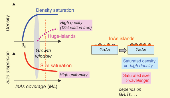
Figure 9.1 A schematic diagram of InAs island density and size depending on InAs coverage.
As a typical example, we show below the structural changes of InAs islands depending on the growth rate [25]. Figure 9.2(a) shows the change in density and size (base diameter) of InAs islands with the growth rate as evaluated by atomic force microscopy (AFM). The growth rate of InAs was varied in the range of 0.1 µm h−1 (0.1 ML s−1) to 0.002 µm h−1 (0.002 ML s−1). In order to keep the V/III ratio constant, the As beam intensity was changed according to the growth rate of InAs (In beam intensity). The growth sequence involved a simultaneous supply of In and As and post‐annealing for 90 s after In supply. In the sample structure, as shown in Figure 9.2(b), InAs islands were grown on the GaAs/AlGaAs/GaAs buffer layers, and buried with GaAs/AlGaAs/GaAs layers; subsequently, on the outermost surface, the InAs islands were grown again under the same conditions, in order to observe the island structure by AFM. The island size (base diameter) and density changed greatly with the growth rate. As the growth rate decreased, the island size increased monotonically and the density decreased drastically. This behavior can be qualitatively explained as follows. The S–K growth mode is understood to change its form so as to lower the total energy given by the sum of the surface energy and the strain energy. The strain is relaxed by island formation and the total energy is reduced. InAs supplied to the surface increases the strain energy on the layered surface but it is possible to reduce the energy by incorporating InAs into the growing islands where the strain is relaxed. When a sufficiently long time for surface migration is available, In atoms on the surface are captured by the growing islands and the island size increases. Conversely, when the surface migration time is short, it is impossible for In atoms to reach the growing islands, and thus new growth islands are formed to relieve the strain and the number of islands grown increases without considerably increasing the size.
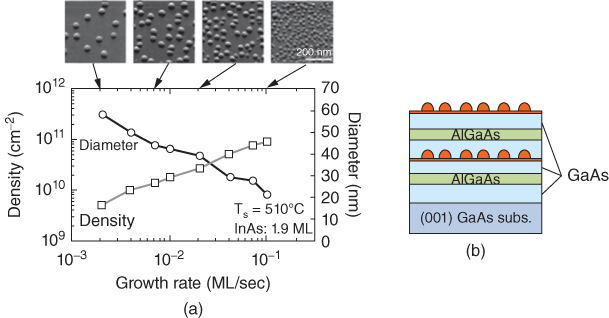
Figure 9.2 (a) Size (base diameter) and density of the InAs islands measured by AFM as a function of the growth rate, together with the corresponding AFM images (0.5 × 0.5 µm2). (b) A schematic diagram of the sample structure.
(Source: After Nakata et al. [26].)
Figure 9.3 shows the PL peak wavelength and its full‐width at half‐maximum (FWHM) at room temperature (RT) obtained from the same samples. The emission wavelength increased as the growth rate decreased and reached a value of 1.3 µm at a growth rate of 0.002 ML s−1. The FWHM decreased with decreasing growth rate, reaching values smaller than 40 meV. Because the FWHM mainly reflects the distribution of island sizes, the figure shows that the island size dispersion is suppressed at low growth rates. Because the island size (especially the height) increases at low growth rates and the emission wavelength increases, the transition energy fluctuation with respect to the size distribution decreases due to size expansion (height increase).

Figure 9.3 PL peak wavelength and FWHM as a function of growth rate measured at RT.
(Source: After Nakata et al. [26].)
Figure 9.4 shows a (110) cross‐sectional TEM image of InAs islands grown at a growth rate of 0.007 ML s−1. The base diameter of the islands was approximately 20 nm and their height was approximately 6 nm. It is clear that at this low growth rate larger islands were formed compared to the islands grown at the higher growth rate of 0.1 ML s−1 with base diameters of 10−15 nm and heights of 3−5 nm [ 25,27]. In the AFM observation of the islands formed on the outermost surface, the base diameter was 50 nm and the height was 10 nm. This increased size compared to that of buried islands cannot be explained only by the shape effect of the AFM probe. The difference is likely due to the shrinkage of InAs islands when they are buried by GaAs, as In atoms diffuse away from islands during burial.

Figure 9.4 A (110) cross‐sectional TEM image of the islands grown at a growth rate of 0.007 ML s−1. The TEM image shows a base diameter of about 20 nm and a height of 6 nm.
(Source: After Nakata et al. [26].)
As described above, by growing InAs islands at growth rates lower than 0.01 ML s−1, the communication wavelength of 1.3 µm can be reached. However, these islands are not suitable for practical laser applications because the island density is too low (as low as 5 × 109 cm−2) and thus sufficient optical gain is not expected.
9.2.2 Emission Wavelength Control by the Buried Strain Relaxation Layer
In this section, we describe a method for controlling the emission wavelength by controlling peripheral structures such as buried layers of islands [26]. This enables control of practical wavelengths while maintaining a density of islands at which a high optical gain is expected.
By burying InAs islands with a strained layer such as InGaAs, lattice strain in the vertical direction is relaxed and the emission wavelength becomes longer compared to that obtained with a GaAs layer. This buried InGaAs layer is called a strain‐reducing layer (SRL) [28]. Figure 9.5 shows the PL peak wavelength obtained from InAs islands buried with InxGa1−xAs layers with different compositions, x, and thicknesses, t [26]. Figure 9.5(a) shows results for 0 < x < 0.2 and t = 8 nm, whereas Figure 9.5(b) displays results for 0 < t < 12 nm and x = 0.17. The sample structures are shown in the insets. As shown in Figure 9.5(a), the emission wavelength became longer for increasing values of x, and reached a value of 1.33 µm at x = 0.2. The emission wavelength from the structure buried with GaAs (i.e. x = 0) was 1.26 µm, and it was possible to shift the emission wavelength by 70 nm by changing the buried layer composition to x = 0.2. As shown in Figure 9.5(b), a tendency to increase the wavelength with the thickness of the InGaAs layer was also confirmed (e.g. the wavelength increased by 60 nm when t increased from 0 to 6 nm). However, the wavelength hardly changed and saturated for t > 6 nm. The thickness of 6 nm is roughly equal to the height of the islands and thus this saturation is considered to occur when the islands are completely covered by the InGaAs layer.
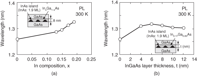
Figure 9.5 (a) PL peak wavelength as a function of In composition, x, in the InGaAs buried layers and (b) as a function of thickness, t, of the InGaAs buried layers. Insets are schematic diagrams of sample structures.
(Source: After Nakata et al. [26].)
Figure 9.6(a−d) shows cross‐sectional field emission‐scanning transmission electron microscope (FE‐STEM) images together with data of the In composition profiles measured by energy dispersive X‐ray spectroscopy (EDS) [26]. Two samples were grown: one where InAs islands were buried with a GaAs layer [Figure 9.6(a, b)] and another one where InAs islands were buried with an 8‐nm‐thick In0.17Ga0.83As layer [Figure 9.6(c, d)]. The In composition profiles were measured along the white lines shown in the FE‐STEM images from the left side to the right side, corresponding to the surface side and the substrate side, respectively. In Figure 9.6(b, d), the center part of the InAs islands (labeled “Dot”) was probed, whereas in Figure 9.6(a, c) the wet layer or the InGaAs buried layer regions (labeled “WL” and “EL”) were probed. The interference fringes of the STEM samples confirmed that the thicknesses of all observation samples was almost the same, and it was possible to compare their compositions. As shown in Figure 9.6(d), even when buried with an InGaAs layer, InAs islands were formed, much like those in Figure 9.6(b), just above the GaAs underlayer. Although some differences are visible in the buried layer region, there are no significant differences between the In composition profile of the InAs islands in Figure 9.6(b, d) in the region near the GaAs underlayer. This indicates that island size and composition did not change, even when islands were buried with an InGaAs layer. Therefore, the longer wavelength due to InGaAs burying is not caused by an island size enlargement or a change in the In composition, but by the relaxation of the lattice strain of InAs islands, as pointed out by Nishi et al. [28].
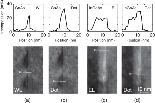
Figure 9.6 In composition profiles of the InAs islands buried with GaAs (a, b) and buried with InGaAs (c, d) measured by EDS, together with the corresponding FE‐STEM images.
(Source: After Nakata et al. [26].)
Figure 9.7(a) is a plan view of a TEM image of InAs islands grown at a low growth rate of 0.007 ML s−1 and buried with a 4‐nm‐thick In0.17Ga0.83As layer [26]. The PL peak wavelength of these InAs islands at room temperature was 1.31 µm. The island density was approximately 2.5 × 1010 cm−2, which was a factor of five higher than that of islands with a 1.3 µm PL peak wavelength created at a low growth rate of 0.002 ML s−1 and embedded by GaAs. Figure 9.7(b) is a cross‐sectional TEM image of the stacked structures [26]. Both InAs island layers were buried with 4‐nm‐thick In0.17Ga0.83As layers and were stacked with a 26‐nm‐thick GaAs intermediate layer. The size and density of the upper island layer is almost the same as that of the first layer (lower layer), indicating that the stacked structures were satisfactorily grown.

Figure 9.7 (a) Plan view of TEM image of the structure when growing islands at a growth rate of 0.007 ML s−1 and buried with a 4‐nm‐thick In0.17Ga0.83 As layer. (b) A (110) cross‐sectional TEM image of the two‐stacked island layers using a 26‐nm‐thick GaAs intermediate layer.
(Source: After Nakata et al. [26].)
9.2.3 InAs Quantum‐Dot Lasers
In this section, we discuss the QD lasers fabricated using InAs islands grown at low growth rates and buried with InGaAs strained layers [ 2629–31].
InAs islands were grown at a growth rate of 0.007 ML s−1 with a nominal thickness of 1.9 ML, and were embedded with a 4‐nm‐thick In0.17Ga0.83As strained layer. The active region was a separate confinement heterostructure (SCH) in which four InAs island layers were stacked via 26‐nm‐thick GaAs intermediate layers and were sandwiched by GaAs layers. A ridge structure with a cavity length of 300 µm was fabricated by chemical etching. Both facets were coated with 95% high‐reflective (HR) films. In continuous wave (CW) oscillation at 25 °C, the oscillation wavelength was 1.31 µm (measured at a current of 6 mA). The threshold current (Ith) was 5.4 mA, which was very low for QD lasers oscillating in this wavelength range. These results have shown that increasing the island density with the stacking technique while maintaining the emission wavelength and emission efficiency are key factors for improving the performance of QD lasers.
Recently, it has been found that In atoms diffuse from the InAs islands during the growth of the buried layer, effectively reducing the island size, shortening the emission wavelength, and degrading the size uniformity (i.e. widening the emission linewidth). By optimizing the embedding conditions, such as the growth temperature and the As pressure, there is a possibility that a higher density of InAs islands emitting in this wavelength region can be formed. In fact, Nishi et al. [32] realized a narrow linewidth of FWHM < 24 meV at emission wavelengths near 1.3 µm by improving the embedding conditions. The island density was approximately 6 × 1010 cm−2, which is considerably high for islands emitting light in this wavelength range. In addition, multiple stacking structures free from defects such as dislocations were grown successively. In lasers using these stacked island structures, high optical gains (54 and 35 cm−1 at 25 and 100 °C, respectively) were obtained from room temperature to high temperatures and it was shown that they can operate even for temperatures as high as 220 °C [33]. In the future, further high‐performance lasers are expected to be realized by improving island and buried layer growth.
9.3 InAs QD Optical Device Operating at Telecom Band (1.55 µm)
Self‐assembled InAs QDs grown on a GaAs substrate initially show emission at ∼1 µm, which is related to the increase of the InAs band gap, caused by the strong compressive strain. Although a 1.3 µm emission of the InAs QDs can be obtained by introducing a strain‐reducing layer [28], it is challenging to obtain a 1.55 µm emission from the InAs QD structure grown on GaAs. On the other hand, InAs QDs grown on an InP substrate are less strained, hence the emission wavelength increases and can reach a value of 1.55 µm. In this section, we discuss the methods used to fabricate an InAs QD structure, with the focus on highly stacked InAs QDs produced by strain‐compensation techniques, and their applications in laser diodes, SOAs, and wavelength tunable lasers. All samples were grown using conventional solid‐source MBE, which provides accurate control of the flux and growth rate.
As mentioned in Section 9.2 , the dome‐shaped InAs QD structures were obtained by self‐assembly during the growth on a GaAs(001) substrate by using a wide range of growth conditions. However, the shape of a self‐assembled InAs nanostructure on an InP(001) substrate is quite different compared to that on a GaAs(001) substrate. For conventional growth conditions, the InAs grown on an InP(001) substrate forms an elongated nanostructure along the [1 −1 0] direction, which is called a quantum dash (QDH) [34]. Although QDHs fix the polarization of light emitted along the surface normal direction, QDs are preferred due to the size uniformity and controllability of their structure. Circular InAs QD structures have been obtained on an InP(311)B substrate [35]. The formation of self‐assembled QDHs on an InP(001) substrate has been explained by the anisotropy of the surface diffusion of adatoms during the crystal growth [36–38]. Therefore, the surface diffusion of adatoms on the InP(311)B substrate is considered to be isotropic.
Figure 9.8 shows an AFM image of InAs QDs grown on an InP(311)B substrate. The surface oxide on the InP(311)B substrate was removed by increasing the substrate temperature to a value of 470 °C in the MBE chamber under As4 irradiation. After the temperature treatment, the lattice‐matched InAlAs buffer layer and InGaAlAs spacer layer were grown, followed by the growth of four monolayers (MLs) InAs. These layers were grown at a temperature of 470 °C. The AFM measurements show that this method produces circular‐shaped InAs QDs with an average height and lateral size of 5 and 35 nm, respectively. Both size and density can be controlled by tuning the growth parameters such as the substrate temperature and growth rate [39]. In addition, the InAs QDs on InP(311)B emit at ∼1550 nm wavelength, and this can be controlled by the size of the QD and the barrier height. Therefore, high‐performance optical devices for fiber‐optic communication systems can be developed using InAs QDs grown on an InP(311)B substrate. For applications in semiconductor lasers or semiconductor amplifiers, the density of QDs should be high, because the QDs act as a gain medium. The density of QDs shown in Figure 9.8 is ∼5 × 1010 cm−2; this can increase up to 1 × 1011 cm−2 by tuning the growth conditions. However, the increase in QD density is limited by spatial restrictions. Assuming the QDs have a diameter of 20 nm and form a closely packed structure, their density would be limited to 3 × 1011 cm−2. In order to further increase the density of QDs, a stacked structure should be considered. The stacked structure is a common method to increase the gain in QWs with a lattice‐matched materials structure. However, self‐assembled QD are obtained by lattice‐mismatched materials systems, hence the accumulation of strain energy becomes an issue during the growth; this is particularly challenging for a stacking with more than 10 layers. However, the strain energy is an important factor, as this acts as a driving force for the self‐assembly process. The accumulated strain energy changes the size and shape of the QDs, and excessive strain energy leads to defects and dislocations which degrade the QDs' crystal quality [40,41].
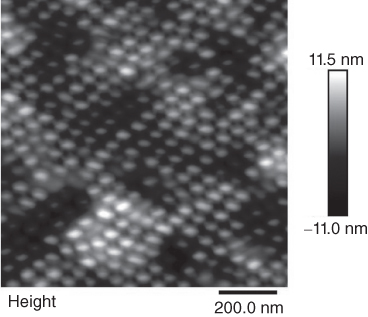
Figure 9.8 AFM image of InAs QDs grown on InP (311)B substrate.
In order to overcome this challenge, strain‐compensation techniques have been developed, where the tensile strain in the QDs layer is compensated by the compressive strain in the capping layer (or spacer layer) [ 35,42]. By using this method, the strain energy can be compensated by the pair of an InAs QD layer and a spacer layer, without limiting the number of stacking layers. For example, 300 InAs QDs layers have been stacked by using the strain‐compensation technique without any degradation of the structure or crystal quality [42]. In this chapter, InGaAlAs (it has a slightly smaller lattice constant compared to that of InP) was used as a strain‐compensation layer on an InP(311)B substrate. The strain‐compensation condition is given by:
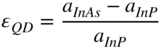
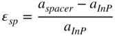
where dQD and dsp denote the thickness of the QD layer and the spacer layer, respectively, while aInAs, aspacer, and aInP are the lattice constants of InAs, InGaAlAs, and InP, respectively. The advantage of this method is that the parameters (such as thickness and composition) of both InAs and spacer layer can be changed even if the strain‐compensation condition is satisfied. Therefore, the QDs' emission wavelength can be controlled by changing the thickness of the InAs or spacer layer, or by changing the composition of the spacer layer; this is of great interest for various device applications.
The detailed structure of a highly stacked QD laser is discussed in Refs. [43,44], where the laser structures have been grown by MBE, as follows. First, an n‐type InAlAs cladding layer was grown on an InP(311)B substrate, and then 20–30 layers of InAs QDs (active region) were grown using the strain‐compensation technique. This was followed by the growth of a p‐type InAlAs cladding layer and a p‐type InGaAs contact layer. After the growth, using conventional ultraviolet (UV) lithography, dry etching, and metal evaporation, the wafer was processed in order to produce a ridge waveguide structure, while the laser cavity was fabricated by cleaving. The fabricated waveguide structure has a width of 2.7 µm and a length of 1 mm. The evaluation of this laser was conducted in a pulsed‐current mode with 2 µs pulse duration and 1% duty; the current–light output (I–L) curve is shown in Figure 9.9. It can be noticed that the threshold current is 77 mA at room temperature (20 °C), which corresponds to a current density of 2.85 kA cm−2. Figure 9.10 shows the spectra before (dotted line) and after (solid line) lasing, measured at an input current of 65 and 111 mA, respectively. The lasing wavelength is 1520 nm, which is close to the peak of the spectrum before the lasing. Therefore, the lasing occurs at the energy level of the QDs' ground states. Some research groups have reported that the lasing occurs at the energy level of the QDs' excited states, because the density of the QDs is not very high [2,3,45]. On the other hand, a highly stacked QD laser has enough density to make the lasing at excited energy levels suppressed.

Figure 9.9 I–L curve of a highly stacked QD laser.

Figure 9.10 Electroluminescence spectra before (dotted line) and after (solid line) lasing measured at an input current of 65 and 111 mA, respectively.
Figure 9.11 shows the temperature dependence of the I–L characteristics for a highly stacked QD laser. The most important feature of QD lasers is the temperature‐independent threshold current. As mentioned before, as the density of states of a QD becomes delta‐function (discrete) shaped and the carrier redistribution is suppressed with increasing temperature, in an ideal QD laser the threshold current is temperature independent. The conventional temperature dependence of the threshold current (Ith) for a semiconductor laser is:

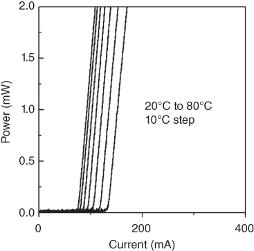
Figure 9.11 Temperature dependence of the I–L curve of a highly stacked QD laser.
where I0, T0, and T denote a constant, characteristic temperature, and measurement temperature, respectively. The large characteristic temperature makes the threshold current almost temperature independent. The highly stacked QD laser has a large characteristic temperature; the maximum value is 160 K for a semiconductor laser operating at 1550 nm telecom band. The improvement of the semiconductor laser's properties is demonstrated not only by the temperature independence but also by the speed of direct modulation, short pulse generation, and high‐frequency repetition in mode‐locked lasers.
Self‐assembled QDs are also of interest for applications in SOAs. The pattern effect present in amplified signals, which is usually observed in bulk or QW‐based SOAs, is expected to be suppressed in QD‐SOAs. A QD‐SOA operating at 1550 nm telecom band has been developed in Ref. [7], where the 40 Gbps high‐speed signal was amplified without pattern effects, due to the high‐speed carrier dynamics of QD‐SOAs. The obtained chip gain and saturation power were over 25 dB and 20 dBm, respectively, which is suitable for applications in fiber‐optic communication systems. In addition, highly stacked QDs have also been employed to fabricate SOAs and obtain a module gain larger than 25 dB. In particular, an extremely high‐speed response of ∼220 Gbps is demonstrated in Ref. [46].
Another application as a light source is in “two‐mode lasers,” which can be used to generate millimeter and terahertz electromagnetic waves. Usually, if the separation is constant, there is a beat signal between two or a few laser lines (multimode lasing). However, when the gain material is in bulk or a QW, there is a “mode competition” for these modes, as the carriers' density of states in such a case is continuous. Therefore, the millimeter and terahertz waves will be unstable. On the other hand, the mode competition should be suppressed in QD lasers because of the discrete energy levels of the QD carriers.
An example of a two‐mode laser consisting of an external cavity that includes a QD gain chip, etalon filter, wavelength tunable band pass filter, and end mirror is shown in Figure 9.12. For this configuration, the mode separation is determined by the etalon filter, while the two modes are chosen by using a band pass filter. The obtained two‐mode lasing spectrum is shown in Figure 9.13. A stable two‐mode emission was observed at around 1541 nm. The actual mode separation of these two modes is 89.5 GHz, which is expected taking into account the design of the etalon filter. The difference in intensity between the two modes is almost zero, while the side‐mode suppression ratio is over 50 dB. The simultaneousness of these two emissions, instead of mode hopping, was confirmed by measuring the beat signal using Michelson interferometry. Moreover, the separation between the two modes can be tuned by the etalon filter. Indeed, two mode emissions with a separation of 300 GHz and 1 THz were obtained, as shown in Figure 9.14. In addition, a millimeter wave was generated by combining the two‐mode laser with a high‐speed uni‐traveling carrier photodiode (UTC‐PD). These results reveal that the systems employed for producing millimeter and terahertz waves can be miniaturized.
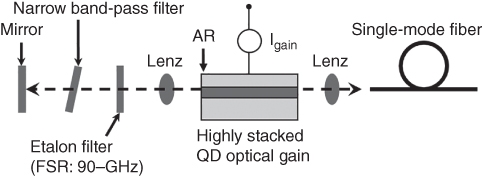
Figure 9.12 Schematic of an external cavity QD laser for two‐mode lasing.

Figure 9.13 Two‐mode lasing spectrum with a mode separation of 90 GHz.
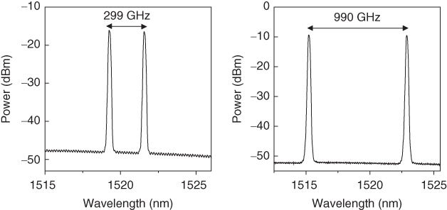
Figure 9.14 Two‐mode lasing spectra with 299 GHz (left) and 990 GHz (right) separation.
In addition to the applications in emitting devices, QDs find applications in detective devices such as photodetectors and solar cells. For such devices, high‐density QDs are advantageous in achieving high performance, hence the increase in QD density by strain compensation becomes important. There is an obvious advantage in using QDs as an absorption material in avalanche photodiodes (APDs), where InGaAs is commonly used for the absorption layer operating at 1550 nm wavelength region telecom band. APDs require a high reversed bias in order to achieve a multiplication of the electric signal, however, this is restricted by the InGaAs breakdown voltage. On the other hand, as the QDs in a QD‐APD structure can absorb light at 1550 nm wavelength region, an electric field is applied to the barrier layer of the QD layer which has a larger band gap than that of InGaAs. This can increase the value of the QD‐APD applied voltage compared to that for a conventional APD. Therefore, QD‐APDs can operate at a higher voltage and can achieve a higher multiplication factor [47]. In addition, QDs are employed for the absorption layer of solar cells and are expected to increase the efficiency of the conversion from sunlight to electrical power.
9.4 Recent Progress in QD Lasers
Since the development of the first QD laser 20 years ago, researchers have investigated the advanced applications of QD lasers as well as the fabrication of hybrid integrated structures for silicon photonics. The improvement of a QD‐laser diode (QD‐LD) operating at 1.55 µm wavelength was achieved in Refs. [48,49], where a high‐speed direct modulation and a narrow linewidth were demonstrated in distributed feedback (DFB) lasers. In the high‐speed modulation laser, 35 Gbps direct modulation was achieved. In addition, such lasers can operate up to a temperature of 125 °C, facilitating temperature‐stable operation. For the narrow‐linewidth lasers, an integrated DFB structure was adapted, and a linewidth of 150 kHz was achieved.
A micro‐disk laser excited by a current injection is reported in Ref. [50], where an InAs QDs structure was grown on a GaAs substrate, with an emission at the 1.3 µm wavelength region. The micro‐disk cavity with a diameter ranging from 15 to 31 µm was fabricated using plasma chemical etching of deep cylindrical mesas. This laser showed lasing with a threshold current of 1.6 mA in continuum current mode, at room temperature. The research on QD lasers integrated on silicon wafers proceeds in two directions: direct growth of III–V materials on Si wafers and wafer bonding of a III–V material and Si. In Ref. [51], a low threshold current characteristic was shown for an InAs QD laser grown directly on a Si substrate. In their study, InAs QDs are used for the dislocation filter at the interface between the III–V material and Si, as well as for the gain medium at the active region. In the dislocation filter region, the InAs QDs adopt the dislocations, hence the number of dislocations in the III–V materials (grown on top of this layer) can be decreased. In addition, the authors reported the optimization of the annealing process performed after growth. They showed that the threshold current of the ridge waveguide laser with a width of 10 µm and a length of 3 mm is ∼100 mA (in pulsed operating mode) and that the lasing wavelength is 1280 nm. The reduction in threshold current (continuous‐wave operating mode) is the subject of future study. On the other hand, the wafer‐bonding method showed better characteristics. In Ref. [52], a QD laser structure with eight QD layers was bonded on a silicon‐on‐insulator (SOI) wafer using oxygen plasma treatment in which the Si waveguide had been fabricated. The length of the QD gain region and that of the Si waveguide were 2 and 3 mm, respectively. The optical gain of the QDs was coupled to the Si waveguide and showed lasing in the Si waveguide. This hybrid structure shows lasing with a threshold current of 35 mA and a lasing wavelength of 1300 nm at room temperature, in continuous‐wave operating mode. In addition, the lasing for this device can be observed up to a temperature of 100 °C.
In Ref. [53], a QD laser structure with eight QD layers was bonded on a Si substrate by using the UV ozone method. Subsequently, the ridge waveguide was fabricated and the wafer was cleaved in order to produce a cavity mirror with a length of 500 µm. This device shows lasing with a threshold current of 41 mA at room temperature, and continuous‐wave operating mode. In addition, this laser shows an ability to operate at high temperatures (up to 60 °C) and achieve a high‐speed direct modulation of 6 Gbps. In Ref. [54], a novel laser is reported, where InGaAs QDs are embedded in a GaAs nanowire. The nanowire has a diameter of 180 nm and acts as a very small optical cavity. The lasing wavelength varies from 840 to 860 nm, starting from low temperatures up to a temperature of 125 K. For this device, although the excitation is achieved by optical pumping, a very small volume and low power consumption are expected. There is ongoing research on the improvement of the performance of QD lasers and their applications.
9.5 Summary
In this chapter, applications of III–V semiconductor QDs in optoelectronic devices were discussed. In particular, we focused on semiconductor QD lasers. The InAs QD lasers grown on GaAs and InP substrates were explained, both of which showed temperature‐stable characteristics based on the change in density of states of carriers in QDs. In addition, combinations of QD technology and others (such as Si photonics) have shown great progress.
References
- 1 Arakawa, H. and Sakaki, H. (1982). Applied Physics Letters 40: 939.
- 2 Huang, X., Stintz, A., Hains, C.P. et al. (2000). IEEE Photonics Technology Letters 12: 227.
- 3 Wang, J.S., Hsiao, R.S., Chen, J.F. et al. (2005). IEEE Photonics Technology Letters 17: 1590.
- 4 Liu, C.Y., Yoon, S.F., Cao, Q. et al. (2007). Applied Physics Letters 90: 041103.
- 5 Kovsh, A.R., Maleev, N.A., Zhukov, A.E. et al. (2002). Electronics Letters 38: 1104.
- 6 Ishida, M., Hatori, N., Akiyama, T. et al. (2004). Applied Physics Letters 85: 4145.
- 7 Sugawara, M., Hatori, N., Ishida, M. et al. (2005). Journal of Physics D 38: 2126.
- 8 Saito, H., Nishi, K., Kamei, A., and Sugou, S. (2000). IEEE Photonics Technology Letters 12: 1298.
- 9 Goldstein, L., Glas, F., Marzin, J.Y. et al. (1985). Applied Physics Letters 47: 1099.
- 10 Kirstaedter, N., Ledentsov, N.N., Grundmann, M. et al. (1994). Electronics Letters 30: 1416.
- 11 Shoji, H., Mukai, K., Ohtsuka, N. et al. (1995). IEEE Photonics Technology Letters 7: 1385.
- 12 Kamath, K., Bhattacharya, P., Sosnowski, T. et al. (1996). Electronics Letters 32: 1374.
- 13 Mirin, R., Gossard, A., and Bowers, J. (1996). Electronics Letters 32: 1732.
- 14 Stranski, I.N. and Krastanow, L. (1937). Akademie der Wissenschaften in Wien. Mathematisch‐Naturwissenschaftliche Klasse‐IIb 146: 797.
- 15 Schaffer, W.J., Lind, M.D., Kowalczyk, S.P., and Grant, R.W. (1983). Journal of Vacuum Science and Technology B1: 688.
- 16 Lewis, B.F., Lee, T.C., Grunthaner, F.J. et al. (1984). Journal of Vacuum Science and Technology B2: 419.
- 17 Glas, F., Guill, C., Henoc, P., and Houzay, F. (1987). Institute of Physics Conference Series 87: 87.
- 18 Houzay, F., Guille, C., Moisson, J.M. et al. (1987). Journal of Crystal Growth 81: 67.
- 19 Berger, P.R., Chang, K., Bhattacharya, P. et al. (1988). Applied Physics Letters 53: 684.
- 20 Guha, S., Madhukar, A., and Rajkumar, K.C. (1990). Applied Physics Letters 57: 2110.
- 21 Tabuchi, M., Noda, S., and Sasaki, A. (1992). Science & Technology of Mesoscopic Structures, 379. New York: Springer.
- 22 Leonard, D., Krishnamurthy, M., Reaves, C.M. et al. (1993). Applied Physics Letters 63: 3203.
- 23 Arakawa, Y. and Yariv, A. (1986). IEEE Journal of Quantum Electronics QE‐22: 1887.
- 24 Grabow, M.H. and Gilmer, G.H. (1988). Surface Science 194: 333.
- 25 Shoji, H., Nakata, Y., Mukai, K. et al. (1996). Japanese Journal of Applied Physics 35: L903.
- 26 Nakata, Y., Mukai, K., Sugawara, M. et al. (2000). Journal of Crystal Growth 208: 93.
- 27 Tackeuchi, A., Nakata, Y., Muto, S. et al. (1995). Japanese Journal of Applied Physics 34: L405.
- 28 Nishi, K., Saito, H., and Sugou, S. (1999). Applied Physics Letters 74: 1111.
- 29 Mukai, K., Nakata, Y., Ohtsubo, K. et al. (1999). IEEE Photonics Technology Letters 11: 1205.
- 30 Mukai, K., Nakata, Y., Ohtsubo, K. et al. (2000). Applied Physics Letters 76: 3349.
- 31 Mukai, K., Nakata, Y., Ohtsubo, K. et al. (2000). IEEE Journal of Quantum Electronics 36: 472.
- 32 Nishi, K., Kageyama, T., Yamaguchi, M. et al. (2013). Journal of Crystal Growth 378: 459.
- 33 Kageyama, T., Takada, K., Nishi, K. et al. (2012). Proceedings of SPIE 8277: 82770C‐1.
- 34 Akahane, K., Yamamoto, N., Gozu, S.I. et al. (2008). Physica E 40: 1916.
- 35 Akahane, K., Ohtani, N., Okada, Y., and Kawabe, M. (2002). Journal of Crystal Growth 245: 31.
- 36 Li, H., Zhuang, Q., Kong, X. et al. (1999). Journal of Crystal Growth 205: 613.
- 37 Stintz, A., Rotter, T.J., and Malloy, K.J. (2003). Journal of Crystal Growth 255: 266.
- 38 Sritirawisarn, N., van Otten, F.W.M., Eijkemans, T.J., and Nötzel, R. (2007). Journal of Crystal Growth 305: 63.
- 39 Akahane, K. and Yamamoto, N. (2013). Journal of Crystal Growth 378: 450.
- 40 Shiramine, K., Horisaki, Y., Suzuki, D. et al. (1998). Japanese Journal of Applied Physics 37: 5493.
- 41 Kim, K.M., Park, Y.J., Roh, C.H. et al. (2003). Japanese Journal of Applied Physics 42: 54.
- 42 Akahane, K., Yamamoto, N., and Kawanishi, T. (2011). Physica Status Solidi A 208: 425.
- 43 Akahane, K., Yamamoto, N., and Tsuchiya, M. (2008). Applied Physics Letters 93: 041121.
- 44 Akahane, K., Yamamoto, N., and Kawanishi, T. (2010). IEEE Photonics Technology Letters 22: 103.
- 45 Markus, A., Chen, J.X., Paranthoën, C. et al. (2003). Applied Physics Letters 82: 1818.
- 46 Matsumoto, A., Akahane, K., Sakamoto, T. et al. (2017). Physica Status Solidi A 214: 1600557.
- 47 Umezawa, T., Akahane, K., Kanno, A., and Kawanishi, T. (2014). Applied Physics Express 7: 032201.
- 48 Banyoudeh, S., Eyal, O., Abdollahinia, A. et al. (2017). Proceedings of SPIE 10123: 1012306.
- 49 Becker, A., Sichkovskyi, V., Bjelica, M. et al. (2017). Applied Physics Letters 110: 181103.
- 50 Kryzhanovskaya, N.V., Maximov, M.V., Blokhin, S.A. et al. (2016). Semiconductors 50: 390.
- 51 Orchard, J.R., Shutts, S., Sobiesierski, A. et al. (2016). Optics Express 24: 6196.
- 52 Kurczveil, G., Liang, D., Fiorentino, M., and Beausoleil, R.G. (2016). Optics Express 24: 16167.
- 53 Jhang, Y.H., Mochida, R., Tanabe, K. et al. (2016). Optics Letters 24: 18428.
- 54 Ho, J., Tatebayashi, J., Sergent, S. et al. (2016). Nano Letters 16: 2845.