In September 2007, the Guinness Book of World Records announced the new record holder for the world’s most powerful distributed computing system. It wasn’t a traditional cluster of high-performance computers, but a worldwide network composed of regular PCs and PlayStation 3 consoles (PS3s). Called Folding@Home, this distributed computing system simulates protein folding to analyze how diseases originate.
Before the PS3s joined in, the network was capable of only .25 petaflops (250,000,000,000,000 floating-point operations per second). But when the Folding@Home client started running on PS3s, the computation speed quadrupled in six months, making Folding@Home the first distributed computing system to break the 1 petaflop barrier.
Table 1.1 clarifies the significance of the PS3s in the Folding@Home network. There aren’t nearly as many consoles as PCs, but they provide more computational power than the Windows/Mac/Linux computers combined.
The PS3’s tremendous computational power is provided by the Cell Broadband Engine, commonly called the Cell processor or just the Cell. Developed by the STI Alliance (Sony, Toshiba, and IBM), the Cell combines the general-purpose capability of IBM’s PowerPC architecture with enough number crunching to satisfy even the most demanding gamers and graphic developers.
What does this mean for you? It means you can enjoy the best of both worlds: computational flexibility and power. On one hand, you can install a common operating system, such as Linux, on the Cell and execute applications as conveniently as if they were running on a PC. On the other hand, you can implement computationally intense algorithms at speeds that far exceed regular CPUs and even compete with supercomputing devices.[1] More incredibly still, you can do both at the same time.
The Cell makes this possible through an on-chip division of labor: The operating system runs on a single PowerPC Processor Element (PPE), and the high-speed calculation is performed by a series of Synergistic Processor Elements (SPEs). These two types of cores are specifically designed for their tasks, and each supports a different set of instructions.
Taken individually, these processing elements are easy to understand and straightforward to program. The hard part is coordinating their operation to take the fullest advantage of their strengths. To accomplish this, a coder must know the Cell-specific programming commands and have a solid knowledge of the device’s architecture: its processing elements, interconnections, and memory structure.
The purpose of this book is to cover these subjects in enough depth to enable you to create applications that maximize the Cell’s capabilities. Much of this treatment delves into the processor’s architecture, but only the aspects that you can use and configure in code. Some topics may seem overwhelming for those not used to thinking like computer architects, but don’t be concerned: Everything will be explained as the need arises. And the goal of this book is always software.
The goal of this chapter is to explain, at a basic level, what the Cell processor is and how it works. The discussion begins with a description of the Cell’s background, including its history and capabilities, and proceeds to introduce the processor’s basic architecture.
The Cell is so unlike its predecessors that it helps to know about why it was created and the corporate forces that shaped its design. When you see why the STI Alliance spent so much time and effort on the Cell, you’ll have a better idea why learning about it is worth your own.
Sony finished development of the PlayStation 2 in 1999 and released it the following year. Despite its tremendous success, then-CEO Nobuyuki Idei was nervous: How could Sony’s next-generation console top the PS2? What more could they accomplish? The answer, he decided, was twofold: The next offering had to integrate broadband multimedia capability and provide dramatic improvements in graphical processing. These lofty goals required entirely new hardware, and to make this possible, he conferred with IBM’s then-CEO, Louis Gerstner. Together they shaped the concept that would ultimately lead to the Cell Processor.
The chief of Sony Computer Entertainment, Ken Kutaragi, fleshed out the hardware requirements and made demands that went far beyond the state of the art. Envisioning each processor as a building block of a larger, networked entity, Ken Kutaragi called the device the Cell. In keeping with Nobuyuki-san’s original intention, the project became called the Cell Broadband Engine (CBE). This remains the official name of the Cell processor.
Toshiba expressed an interest in using the Cell in their consumer electronics, and in 2001, Sony, Toshiba, and IBM announced the formation of the STI Alliance. Their stated intention was to research, develop, and manufacture a groundbreaking processor architecture. They formed the STI Design Center in Austin, Texas, to turn the CBE’s requirements into reality.
As the Cell’s chief architect, Jim Kahle saw that the CBE’s requirements couldn’t be met with a traditional single-core processor—the demand for power would be too great. Instead, he chose a more power-efficient design that incorporated multiple processing units into a single chip. The final architecture consisted of nine cores: one central processing element and eight dedicated elements for high-speed computation.
At the time of this writing, the STI Design Center has grown to more than 400 engineers. Dr. H. Peter Hofstee, one of the Cell’s founding designers, holds the positions of chief scientist and chief architect of the SPE. In a recent presentation, he listed the main goals that drove the Cell’s design:
Outstanding performance on gaming and multimedia applications
Real-time responsiveness to the user and the network
Applicability to a wide range of platforms
In 2004, IBM’s semiconductor manufacturing plant in East Fishkill produced the first Cell prototype. The STI engineers installed Linux and tested the processor at speeds beyond the commonly stated range of 3 to 4GHz. The prototype passed. Over the next year, Sony and IBM worked feverishly to integrate the device within Sony’s next-generation console, and expectant gamers caught their first glimpse of the PlayStation 3 at the 2005 Electronic Entertainment Expo (E3).
November 2006 marked the full commercial release of the PS3, and the tales of long lines and barely sane consumers will amuse retail personnel for years to come. In addition to its powerful Cell processor brain, the new console provided resolution up to 1080p and a Blu-ray drive for high-definition video.
That same year, IBM released its first CBE Software Development Kit (SDK) to enable developers to build applications for the Cell. The SDK provides compilers for both types of processing elements, a combined simulator/debugger, numerous code libraries, and an Eclipse-based development environment. A great deal of this book is concerned with the SDK and how you can use it to build applications.
In mid-2008, the first Cell-based supercomputer, called the IBM Roadrunner, was tested in the Los Alamos National Laboratory. Containing 12,960 Cell processors and 12,960 Opterons, the Roadrunner reached a processing speed of 1.026 petaflops and has become the fastest of the supercomputers on the TOP500 list. Its speed more than doubles that of the second-place supercomputer, BlueGene/L, at .478 petaflops.
In 2005, the Lawrence Berkeley National Laboratory studied the Cell’s computational performance and recorded their findings in the report The Potential of the Cell Processor for Scientific Computing. They simulated a number of different algorithms and compared the Cell’s processing speed to that of similar processors: the AMD Opteron, Intel’s Itanium2, and Cray’s X1E. Table 1.2 tabulates their results.
Table 1.2. Results of the Lawrence Berkeley National Laboratory Study (All Values in Gflops/s)
Cell Processor | Cray X1E | AMD Opteron | Intel Itanium2 | |
|---|---|---|---|---|
Dense matrix multiply (single precision) | 204.7 | 29.5 | 7.8 | 3.0 |
Dense matrix multiply (double precision) | 14.6 | 16.9 | 4.0 | 5.4 |
Symmetric sparse matrix vector multiply (single precision)[1] | 7.68 | — | .80 | .83 |
Symmetric sparse matrix vector multiply (double precision)[1] | 4.00 | 2.64 | .60 | .67 |
Nonsymmetric Sparse Matrix Vector Multiply (Single Precision)[1] | 4.08 | — | .53 | .41 |
Nonsymmetric sparse matrix vector multiply (double precision)[1] | 2.34 | 1.14 | .36 | .36 |
2-D fast Fourier transform (single precision)[2] | 40.5 | 8.27 | .34 | .15 |
2-D fast Fourier transform (double precision)[2] | 6.7 | 7.10 | .19 | .11 |
[1] Sparse matrix results averaged from samples in the SPARSITY suite of matrices. [2] 2-D FFTs performed with 2K x 2K array sizes. | ||||
There are two points to keep in mind. First, the results refer to the computation speed in billions of flops (floating-point operations per second), not the amount of time needed to perform the algorithm. Second, because the first-generation Cell’s multipliers are single precision, the first-generation Cell performs much better with single-precision values than with double-precision values. But the second generation provides hardware multiplication of double-precision values.
To an engineer interested in signal processing and computational mathematics (like myself), the results are nothing short of astounding. The study justifies the outrageous marketing claims: The Cell really provides supercomputer-like capability for nearly the cost and power (approximately 50 to 60 W) of a regular CPU.
In Randall Hyde’s fine series of books, Write Great Code, one of his fundamental lessons is that, for optimal performance, you need to know how your code runs on the target processor. Nowhere is this truer than when programming the Cell. It isn’t enough to learn the C/C++ commands for the different cores; you need to understand how the elements communicate with memory and one another. This way, you’ll have a bubble-free instruction pipeline, an increased probability of cache hits, and an orderly, nonintersecting communication flow between processing elements. What more could anyone ask?
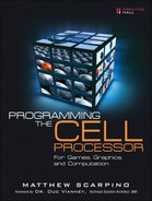
Figure 1.1 shows the primary building blocks of the Cell: the Memory Interface Controller (MIC), the PowerPC Processor Element (PPE), the eight Synergistic Processor Elements (SPEs), the Element Interconnect Bus (EIB), and the Input/Output Interface (IOIF). Each of these is explored in greater depth throughout this book, but for now, it’s a good idea to see how they function individually and interact as a whole.
The MIC connects the Cell’s system memory to the rest of the chip. It provides two channels to system memory, but because you can’t control its operation through code, the discussion of the MIC is limited to this brief treatment. However, you should know that, like the PlayStation 2’s Emotion Engine, the first-generation Cell supports connections only to Rambus memory.
This memory, called eXtreme Data Rate Dynamic Random Access Memory, or XDR DRAM, differs from conventional DRAM in that it makes eight data transfers per clock cycle rather than the usual two or four. This way, the memory can provide high data bandwidth without needing very high clock frequencies. The XDR interface can support different memory sizes, and the PlayStation 3 uses 256MB of XDR DRAM as its system memory.
The PPE is the Cell’s control center. It runs the operating system, responds to interrupts, and contains and manages the 512KB L2 cache. It also distributes the processing workload among the SPEs and coordinates their operation. Comparing the Cell to an eight-horse coach, the PPE is the coachman, controlling the cart by feeding the horses and keeping them in line.
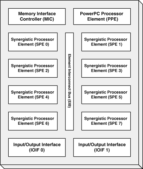
As shown in Figure 1.2, the PPE consists of two operational blocks. The first is the PowerPC Processor Unit, or PPU. This processor’s instruction set is based on the 64-bit PowerPC 970 architecture, used most prominently as the CPU of Apple Computer’s Power Mac G5. The PPU executes PPC 970 instructions in addition to other Cell-specific commands, and is the only general-purpose processing unit in the Cell. This is why Linux is installed to run on the PPU and not on the other processing units.

But the PPU can do more than just housekeeping. It contains IBM’s VMX engine for Single Instruction, Multiple Data (SIMD) processing. This means the PPU can operate on groups of numbers (e.g., multiply two sets of four floating-point values) with a single instruction. The PPU’s SIMD instructions are the same as those used in Apple’s image-processing applications, and are collectively referred to as the AltiVec instruction set. Chapter 8, “SIMD Programming on the PPU, Part 1: Vector Libraries and Functions,” is dedicated to AltiVec programming on the PPU.
Another important aspect of the PPU is its capacity for symmetric multithreading (SMT). The PPU allows two threads of execution to run at the same time, and although each receives a copy of most of the PPU’s registers, they have to share basic on-chip execution blocks. This doesn’t provide the same performance gain as if the threads ran on different processors, but it allows you to maximize usage of the PPU resources. For example, if one thread is waiting on the PPU’s memory management unit (MMU) to complete a memory write, the other can perform mathematical operations with the vector and scalar unit (VXU).
The second block in the PPE is the PowerPC Processor Storage Subsystem, or PPSS. This contains the L2 cache along with registers and queues for reading and writing data. The cache plays a very important role in the Cell’s operation: not only does it perform the regular functions of an L2 cache, it’s also the only shared memory bank in the device. Therefore, it’s important to know how it works and maintains coherence. Chapter 6, “Introducing the PowerPC Processor Unit (PPU),” covers this topic in greater depth.
The PPU is a powerful processor, but it’s the Synergistic Processor Unit (SPU) in each SPE that makes the Cell such a groundbreaking device. These processors are designed for one purpose only: high-speed SIMD operations. Each SPU contains two parallel pipelines that execute instructions at 3.1GHz. In only a handful of cycles, one pipeline can multiply and accumulate 128-bit vectors while the other loads more vectors from memory.
SPUs weren’t designed for general-purpose processing and aren’t well suited to run operating systems. Instead, they receive instructions from the PPU, which also starts and stops their execution. The SPU’s instructions, like its data, are stored in a unified 256KB local store (LS), shown in Figure 1.3. The LS is not cache; it’s the SPU’s own individual memory for instructions and data. This, along with the SPU’s large register file (128 128-bit registers), is the only memory the SPU can directly access, so it’s important to have a deep understanding of how the LS works and how to transfer its contents to other elements.
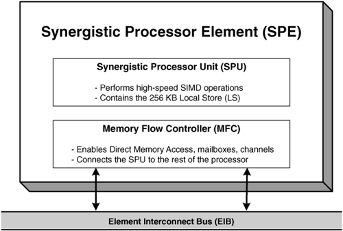
The Cell provides hardware security (or digital rights management, if you prefer) by allowing users to isolate individual SPUs from the rest of the device. While an SPU is isolated, other processing elements can’t access its LS or registers, but it can continue running its program normally. The isolated processor will remain secure even if an intruder acquires root privileges on the PPU. The Cell’s advanced security measures are discussed in Chapter 14, “Advanced SPU Topics: Overlays, Software Caching, and SPU Isolation.”
Figure 1.3 shows the Memory Flow Controller (MFC) contained in each SPE. This manages communication to and from an SPU, and by doing so, frees the SPU for crunching numbers. More specifically, it provides a number of different mechanisms for interelement communication, such as mailboxes and channels. These topics are discussed in Chapters 12, “SPU Communication, Part 1: Direct Memory Access (DMA),” and 13, “SPU Communication, Part 2: Events, Signals, and Mailboxes.”
The MFC’s most important function is to enable direct memory access (DMA). When the PPU wants to transfer data to an SPU, it gives the MFC an address in system memory and an address in the LS, and tells the MFC to start moving bytes. Similarly, when an SPU needs to transfer data into its LS, it can not only initiate DMA transfers, but also create lists of transfers. This way, an SPU can access noncontiguous sections of memory efficiently, without burdening the central bus or significantly disturbing its processing.
The EIB serves as the infrastructure underlying the DMA requests and interelement communication. Functionally, it consists of four rings, two that carry data in the clockwise direction (PPE > SPE1 > SPE3 > SPE5 > SPE7 > IOIF1 > IOIF0 > SPE6 > SPE4 > SPE2 > SPE0 > MIC) and two that transfer data in the counterclockwise direction. Each ring is 16 bytes wide and can support three data transfers simultaneously.
Each DMA transfer can hold payload sizes of 1, 2, 4, 8, and 16 bytes, and multiples of 16 bytes up to a maximum of 16KB. Each DMA transfer, no matter how large or small, consists of eight bus transfers (128 bytes). As Chapter 12 explains, DMA becomes more efficient as the data transfers increase in size.
As the name implies, IOIF connects the Cell to external peripherals. Like the memory interface, it is based on Rambus technology: FlexIO. The FlexIO connections can be configured for data rates between 400MHz to 8GHz, and with the high number of connections on the Cell, its maximum I/O bandwidth approaches 76.8GB/s. In the PlayStation 3, the I/O is connected to Nvidia’s RSX graphic processor. The IOIF can be accessed only by privileged applications, and for this reason, interfacing the IOIF lies beyond the scope of this book.
This book uses a hands-on approach to teach Cell programming, so the development tools are very important. The most popular toolset is IBM’s Software Development Kit (SDK), which runs exclusively on Linux and provides many different tools and libraries for building Cell applications.
IBM provides the SDK free of charge, although some of the tools have more restrictive licensing than others. For the purposes of this book, the most important aspect of the SDK is the GCC-based toolchain for compiling and linking code. The two compilers, ppu-gcc and spu-gcc, compile code for the PPU and SPU, respectively. They provide multiple optimization levels and can combine scalar operations into more efficient vector operations. Chapter 3, “Building Applications for the Cell Processor,” explores these and the rest of the SDK’s build tools in depth.
The SDK also includes IBM’s Full-System Simulator, tailored for Cell applications. This impressive application runs on a conventional computer and provides cycle-accurate simulation of the Cell processor, keeping track of every thread and register in the PPU and SPUs. In addition to basic simulation and debugging, it provides many advanced features for responding to processing events. Chapter 4, “Debugging and Simulating Applications,” covers the simulator in thorough detail.
The SDK contains many code libraries to ease the transition from traditional programming to Cell development. It provides most standard C/C++ libraries for both the PPU and SPU, POSIX commands for the PPU, and a subset of the POSIX API on the SPU. Many of the libraries are related to math, but others can be used to profile an SPU’s operation, maintain a software cache, and synchronize communication between processing units.
All of these tools and libraries can be accessed through the Cell SDK integrated development environment (IDE). This is an Eclipse-based graphical user interface for managing, editing, building, and analyzing code projects. It provides a powerful text editor for code entry, point-and-click compiling, and a feature-rich interface to the Cell debugger. With this interface, you can watch variables as you step through code and view every register and memory location in the Cell. Chapter 5, “The Cell SDK Integrated Development Environment,” explains the Cell IDE in detail.
Some time ago, I had the pleasure of programming assembly language on a multicore digital signal processor, or DSP. The DSP performed matrix operations much, much faster than the computer on my desk, but there were two problems: I had to write all the routines for resource management and event handling, and there was no file system to organize the data. And without a network interface, it was hard to transfer data in and out of the device.
The Cell makes up for these shortcomings and provides many additional advantages. With SIMD processing, values can be grouped into vectors and processed in a single cycle. With Linux running on the PPE, memory and I/O can be accessed through a standard, reliable API. Most important, when all the SPEs crunch numbers simultaneously, they can process matrices at incredible speed.
The goal of this book is to enable you to build applications with similar performance. As with the DSP, however, it’s not enough just to know the C/C++ functions. You have to understand how the different processing elements work, how they’re connected, and how they access memory. But first, you need to know how to use the tools. The next chapter explains how to acquire and install IBM’s SDK.