Chapter 2
Technical Overview
Abstract
This chapter covers overview of the technical details of ARM® Cortex®-M0 and Cortex-M0+ processor, examples of how they are integrated into a system, the applications, and various factors for using Cortex-M0 and Cortex-M0+ processors including details of technical advantages.
Keywords
Applications of Cortex-M processors; ARMv6-M architecture; Example system designs; Features overview; Key components of the processors; Technical advantages2.1. What are the Cortex®-M0 and Cortex-M0+ Processors?
The ARM® Cortex-M0 processor and Cortex-M0+ processors are both 32-bit processors. Their internal registers in the register banks, data paths, and the bus interfaces are all 32 bit. Both of them have a single main system bus interface, therefore they are considered as Von Neumann bus architecture.
The Cortex-M0+ processor has an optional single cycle I/O interface that is primarily for faster peripheral I/O register accesses. Therefore, it is possible to say the Cortex-M0+ processor has limited Harvard bus architecture capability as instruction access and I/O register accesses could be carried out at the same time, but it is important to understand that although there can be two bus interfaces, the memory space is shared (unified) and therefore the extra bus interface does not bring additional addressable memory space.
The key characteristics of the Cortex-M0 and Cortex-M0+ processors are as follows:
Processor pipeline
• The Cortex-M0 processor has a three-stage pipeline (fetch, decode, and execute)
• The Cortex-M0+ processor has a two-stage pipeline (fetch + predecode, decode + execute)
Instruction set
• The instruction set is based on Thumb® Instruction Set Architecture (ISA). Only a subset of the Thumb ISA is used (56 of them). Most of the instructions are 16 bit in size, only a few of them are 32 bit.
• In general, the Cortex-M processors are classified as Reduced Instruction Set Computing although they have instructions of different sizes.
• Support optional single cycle 32 bit × 32 bit multiply, or a smaller multicycle multiplier for designs that need small silicon area.
Memory addressing
• 32-bit addressing supporting up to 4 GB of memory space
• The system bus interface is based on an on-chip bus protocol called AHB-Lite, supporting 8-bit, 16-bit, and 32-bit data transfers
Interrupt Handling
• The processors include a built-in interrupt controller called the Nested Vectored Interrupt Controller (NVIC). This unit handles interrupt prioritization and masking functions. It supports up to 32 interrupt requests from various peripherals (chip design dependent), an additional Non-Maskable Interrupt (NMI) input, and also support a number of system exceptions.
• Each of the interrupts can be set to one of the four programmable priority levels. NMI has a fixed priority level.
Operating Systems (OS) support
• Two system exception types (SVCall and PendSV) are included to support OS operations.
• An optional 24-bit hardware timer called SysTick (System Tick Timer) is also included for periodic OS time keeping.
• The Cortex-M0+ processor support privileged and unprivileged execution level (optional to chip designers). This allows OS to run some of the application tasks with unprivileged execution level and impose memory access restrictions to these tasks.
• The Cortex-M0+ processor has an optional Memory Protection Unit (MPU) to allow OS to define memory access permission for application tasks during run time.
Low Power support
• Architecturally two sleep modes are defined as normal sleep and deep sleep. The exact behaviors in these sleep modes are device specific (depends on which chip you are using). Chip designers can also add device specific power saving mode control registers to expand the number of sleep modes or to allow the sleep mode behavior for each part of the chip to be defined.
• Sleep mode can be entered using WFI (Wait for Interrupt) or WFE (Wait for Event) instructions, or using a feature called Sleep-on-Exit to allow the processor to enter sleep automatically.
• Additional hardware level supports to enable chip designers to create better power reductions based on the sleep mode features, for example, the Wake-up Interrupt Controller (WIC).
Debug
• The debug system is based on the ARM CoreSight™ Debug Architecture. It is a scalable debug architecture that can support simple-single processor designs to complex multiprocessor designs.
• A debug interface that can either be based on JTAG protocol (4 or five pins), or Serial Wire Debug protocol (2 pins). The debug interface allows software developers to access debug features of the processors.
• Support up to four hardware breakpoints, two data watchpoints, and unlimited software breakpoint using BKPT (breakpoint) instruction.
• The Cortex-M0+ Processor has an optional feature called Micro Trace Buffer (MTB), this provide instruction trace.
The Cortex-M Processors are configurable designs. They are delivered to chip designers in form of Verilog source code files with a number of parameters that chip designers can select. In this way, chip designers can omit some of the features that are unnecessary for their projects to save power and reduce silicon area. As a result, you can find microcontrollers based on the Cortex-M0 and Cortex-M0+ processor with different number of supported interrupts, and Cortex-M0+ processor with and without the optional MPU.
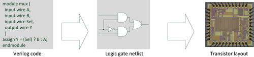
During the design process (Figure 2.1), the processor is integrated with the rest of the system and converted to a design composed of logic gates and then transistors layout using chip design tools. The timing characteristics like maximum clock frequency are defined at these stages based on the semiconductor process selected for the project and various design constraints. In addition, the exact maximum speed and power consumption of the Cortex-M0 or Cortex-M0+ processor on different products can also be different from each other.
2.2. Block Diagrams
A simplified block diagram of the Cortex®-M0 processor is shown in Figure 2.2.
The processor core contains the register banks, ALU, data path, and control logic. It is a three-stage pipeline design with fetch stage, decode stage, and execution stage. The register bank has sixteen 32-bit registers. A few of the registers in the register bank have special usages (e.g., PC). The rest are available for general data processing.
The NVIC accepts up to 32 interrupt request signals and a NMI input. It contains the functionality required for comparing priority between interrupt requests and current priority level so that nested interrupts can be handled automatically. If an interrupt is accepted, the NVIC communicates with the processor so that the processor can execute the correct interrupt handler.
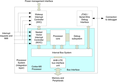
The WIC is an optional unit. In low-power applications, the microcontroller can enter standby state with most parts of the processor powered down. Under this situation, the WIC can perform the function of interrupt masking while the NVIC and the processor core are inactive. When an interrupt request is detected, the WIC informs the power management to power up the system so that the NVIC and the processor core can then handle the rest of the interrupt processing.
The debug subsystem contains various functional blocks to handle debug control, program breakpoints, and data watchpoints. When a debug event occurs, it can put the processor core in a halted state so that embedded developers can examine the status of the processor at that point.
The internal bus system, data path in the processor core, and the AHB-Lite bus interface are all 32-bit wide. AHB-Lite is an on-chip bus protocol used in many ARM® processors. This bus protocol is part of the AMBA® (Advanced Microcontroller Bus Architecture) specification, which is a bus architecture developed by ARM and widely used in the IC design industry.
The JTAG or Serial Wire interface units provide access to the bus system and debugging functionalities. The JTAG protocol is a popular 4-pin (5-pin if including a reset signal) communication protocol commonly used for IC and PCB testing. The Serial Wire protocol is a newer communication protocol that only requires two wires, but it can handle the same debug functionalities as JTAG. As illustrated in the block diagrams (Figures 2.2 and 2.3), the debug interface module is separated from the processor design. This is required in the CoreSight™ Debug Architecture where multiple processors can share the same debug connections. There are a number of additional signals for multiprocessor debug support not shown in the diagrams.
The Cortex-M0+ processor is very similar (as shown in Figure 2.3) to Cortex-M0 processor. The only addition is the adding of the optional MPU, single cycle I/O interface bus and the interface for the MTB. The processor core internal design is also changed to a two-stage pipeline arrangement.

The MPU is a programmable device used to define access permission of the memory map. In some of the applications where an OS is used, application tasks can be executed with an unprivileged execution level with restrict memory access defined by the MPU, which is programmed by the OS.
The single cycle I/O interface provides another bus interface with faster access compared to the AHB-Lite system bus (pipelined operation). The MTB is used to provide instruction trace.
In both Cortex-M0 and Cortex-M0+ processors, a number of components in the processors are optional. For example, the debug support, MPU and the WIC are all optional. Some other components like the NVIC are configurable: allowing chip designers to define the features available, for example, the number of interrupt requests (IRQ).
2.3. Typical Systems
As you can see from the block diagrams, the Cortex®-M0 and Cortex-M0+ processors do not contain memories and peripherals. Chip designers need to add these components to the designs. As a result, different Cortex-M processor-based microcontrollers can have different memory sizes, address map, peripherals, interrupt assignment, etc.
In a simple microcontroller design based on a Cortex-M processor, the design would consist of the following:
• A memory for program code storage, usually a Read-Only-Memory (ROM) component, or reprogrammable memory technologies such as flash memory.
• A read–write memory for data (including variables, stack, etc.), usually based on Static Random Access Memory (SRAM).
• Various types of peripherals.
• Bus infrastructure components for joining the processor to all the memories and peripherals.
In some cases, there can also be a separate ROM device with boot code to boot up the microcontroller before the program in the user flash is executed. This is typically called boot ROM or boot loader.
For a simple design with Cortex-M0 processor, the design could look like the one shown in Figure 2.4.
A typical design based on the Cortex-M0 processor might partition the bus system into two parts, which are as follows:
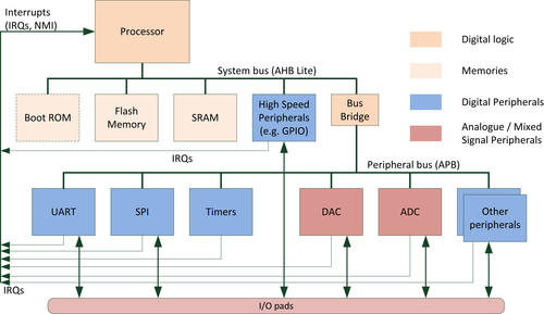
• The peripherals are connected to the peripheral bus, which might have a different operating frequency compared to the system bus.
It is quite common for some of the peripherals to be connected to a separated peripheral bus, which is linked to the main system bus via a bus bridge. This bus protocol for the peripheral bus is typically based on APB, which is a bus protocol defined in the AMBA®.
The uses of a separated APB peripheral bus are as follows:
• Allows lower hardware cost because the APB protocol (non-pipelined operations) is simpler than AHB-Lite (pipelined operations)
• Allows the peripheral bus to run at a different clock frequency than the main system bus
• Avoids large combinational logic in the bus infrastructure for the main system bus, which could become the bottle neck in terms of getting to get high operating frequency. Many peripherals might present in a microcontroller designs and the bus fabric for peripherals can become quite large.
Another group of important connections are the interrupts—A number of peripherals can generate interrupt requests, including the General Purpose Input/Output (GPIO) modules. In most microcontroller designs, external devices connected to certain GPIO pins can generate interrupt request to the processor via some additional conditioning and synchronization logic.

For a system based on the Cortex-M0+ processor, the system design can be very similar, like the one shown in Figure 2.5.
In this design, the high-speed peripherals are moved to the single cycle I/O interface bus for faster I/O performance, and the MTB is added between the AHB-Lite system bus and the SRAM for support instruction trace capture.
Potentially the processor might not be the only component in the system that can generate bus transactions. In many microcontroller products, there is also a component called Direct Memory Access (DMA) controller. Once programmed, the DMA controller can carry out memory accesses on requests from peripherals without processor intervention (Figure 2.6)
The DMA controller can perform data transfers between memory and peripherals, or between memories (e.g., to accelerate memory copy). This is commonly needed for microcontrollers with high bandwidth communication interface like Ethernet or USB. However, it can also benefit some low-power applications, for example, by avoiding waking up the processor from sleep mode to collect small amount of data from peripherals.

2.4. What Is ARMv6-M Architecture?
Both the Cortex®-M0 processor and Cortex-M0+ processor are based on the ARMv6-M architecture. In ARM® processors, the term architecture can refer to the following two areas:
• Architecture: ISA (Instruction Set Architecture), programmer's model (what the software sees) and debug methodology (what the debugger sees). The ARMv6-M is one of the architectures available.
• Microarchitecture: implementation-specific details such as interface signals, instruction execution timing, pipeline stages. Microarchitecture is processor design-specific. For example, the Cortex-M0 processor has a three-stage pipeline microarchitecture.
Various versions of the ARM Architecture exist for different ARM processors released over the years. For example, the Cortex-M3 and Cortex-M4 processors are both implementations of ARMv7-M Architecture. An ISA can be implemented with various implementations of microarchitecture, for example, different number of pipeline stages, different type of bus interface protocol, etc.
The details of the ARMv6-M architecture are documented in the ARMv6-M Architecture Reference Manual (also known as ARMv6-M ARM). This document covers the following:
• Instruction set details
• Programmer's model
• Exception model
• Memory model
• Debug architecture
This document can be obtained from ARM after a simple registration process. However, for general programming, it is not necessary to have the full architecture reference manual. ARM provides alternate documents for software developers called Cortex-M0/M0+/M3/M4/M7 Devices Generic User Guides. This can be found in the ARM Web site:
→ Cortex-M series processors
→ Cortex-M0/M0+/M3/M4/M7
→ Revision number
→ Cortex-M0/M0+/M3/M4/M7 Devices Generic User Guide
Some of the microarchitecture information such as instruction execution timing information can be found in the Technical Reference Manuals of the Cortex-M processors, which can be found on the ARM Web site. Other microarchitecture information like the processor interface details are documented in other Cortex-M product documentation which is normally accessible only by silicon chip designers.
Theoretically, a software developer does not necessarily need to know anything about the microarchitecture to develop software for the Cortex-M products. But in some cases, knowing some of the microarchitecture details could help. This is particularly true for optimizing software or even C compilers for best performance.
2.5. Software Portability Between Cortex®-M Processors
The Cortex-M0, Cortex-M0+, and Cortex-M1 Processors are based on the ARMv6-M Architecture, whereas the Cortex-M3, Cortex-M4, and the Cortex-M7 Processors are based on the ARMv7-M Architecture. As shown in Figure 1.4, they have different instruction set support.
The Cortex-M0 and Cortex-M0+ Processors have the exact same instruction set and similar programmer's model (Cortex-M0+ Processor have optional support for unprivileged execution level and MPU, whereas Cortex-M0 processor does not). However, they have different physical characteristics like instruction timing and have different system features.
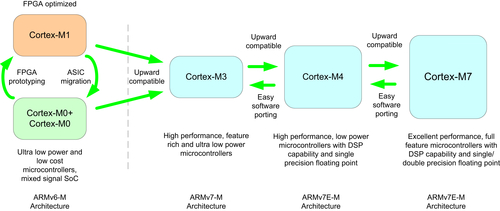
The Cortex-M3 and Cortex-M4 Processors are based on the ARMv7-M architecture and its Thumb®-2 instruction set is a superset of the instruction set used in ARMv6-M. The programmer's model is also similar to ARMv6-M. As a result, in most cases software developed for the Cortex-M0 and Cortex-M0+ can run on the Cortex-M3 and Cortex-M4 Processors without changes, assuming the system has same memory maps and peripherals. The Cortex-M7 processor supports all instructions available in the Cortex-M4 processor, and optionally supports double precision floating point instructions.
The similarity between the Cortex-M processors provides various benefits. First, it provides better software portability. In most cases, C programs can be transferred between these processors without changes. And binary images from Cortex-M0 or Cortex-M1 processors can run on a Cortex-M3 processor due to its upward compatibility (Figure 2.7).
The second benefit is that the similarities between Cortex-M processors allow development tool chains to support multiple processors easily. Apart from similarities on instruction set and programmer's model, the debug architecture is also similar.
The consistency of instruction set and programmer's model also make it easier for embedded programmers to migrate between different products and projects without facing a sharp learning curve.
2.6. The Advantages of the ARM® Cortex®-M0 and Cortex-M0+ Processor
2.6.1. Low Power and Energy Efficiency
One of the key targets of the Cortex-M0 and Cortex-M0+ processors is low power. The result is that the Cortex-M0 processor consumes only 12.5 μW/MHz with 90 nm semiconductor process, or 66 μW/MHz with 180 nm semiconductor process. For the Cortex-M0+ processor, the energy efficiency is even better—only 9.8 μW/MHz with 90 nm semiconductor process, or 50 μW/MHz with 180 nm semiconductor process. This is very low-power consumption for a 32-bit processor. How was this target achieved?
In order to lower the power consumption, ARM had put a lot of effort into various areas to ensure the Cortex-M0 and Cortex-M0+ processors could reach their low-power target. These areas included the following:
• Small gate count
• High efficiency
• Low-power features (e.g., sleep modes)
• Logic cell enhancement
Let us take a look at these areas one by one.
Small Gate Count
The Cortex-M0/M0+ processor's small gate count characteristic directly reduces the active current and leakage current of the processor. During the development of these processors, various design techniques, and optimizations were used to make the circuit size as small as possible. Each part of the design was carefully developed and reviewed to ensure the circuit size is small (it is just a bit like writing an application program in assembly to achieve the best optimization). This allows the gate count to be 12k gates at minimum configuration. In practice, the gate count would be higher when including more features. This is about the same size or smaller than typical 16-bit microprocessors, while having more than double the system performance.
High efficiency
By having a highly efficient architecture, embedded system designers can develop their products so that they can operate at a lower clock frequency while still being able to provide the required performance, reducing the active electric current of the products. This advantage can be used in conjunction with the sleep mode features in the Cortex-M0/M0+ processor so that an embedded system can stay in low-power mode more often to reduce the average power consumption without losing performance.
Sleep Modes and Low-Power Features
The Cortex-M processors have a number of low-power features to allow designers to create very low-power applications. First, the processors have two architectural-defined sleep modes “Sleep” and “Deep sleep.” In normal designs, the number of sleep modes can be further expanded using device-specific power control registers.
The sleep modes can be entered using special instructions—“WFE” and “WFI,” or via “Sleep-on-Exit” feature, which causes the processor to run only when an interrupt service require servicing.
Various hardware level features also allow chip designers to fully utilize their low-power capability of the design. For example, the Cortex-M processors support a unique feature called the WIC, which allows most parts of the processor system to be powered down while still allowing interrupt events to be detected, and allow the systems to resume operation almost instantaneously when required. This greatly reduces the leakage current (static power consumption) of the system during sleep.
In addition, the design of the Cortex-M0 processor is also carefully developed so that some parts of the processor like the debug system can be switched off when it is not required.
Logic Cell Enhancements
In recent years there have been enhancements in logic cell designs. Apart from pushing logic gate designs to smaller transistor size, the Physical IP (Intellectual Property) division in ARM has also been working hard to find innovative ways to reduce power consumption in embedded systems. One of the major developments is the introduction of Ultra Low Leakage (ULL) logic cell library. The first ULL cell library is developed with 0.18 um process. Apart from reducing the leakage current, the new cell library also supports special state retention cells that can hold state information while the rest of the system is powered down. ARM also works with leading EDA tools vendors to allow chip vendors to make use of these new technologies in their chip designs.
2.6.2. High Code Density
Since most of the instructions are only 16-bit in size, the Cortex-M processors have very high code density. This enables an application to be squeezed into a microcontroller with a smaller flash memory. By doing that a designer can use a cheaper microcontroller for the application, and in some cases reduce the power consumption because the flash memory required is smaller.
The smaller flash memory size requirement can also bring additional benefit such as lower electromagnetic interference due to lower power, and smaller silicon package.
2.6.3. Low Interrupt Latency and Deterministic Behavior
In many microcontroller applications, low interrupt latency is an essential requirement. The interrupt latency of the Cortex-M0 processor is only 16 clock cycles and the Cortex-M0+ processor has an interrupt latency of 15 cycles. These latency figures include the stacking of a certain number of registers to the stack, so the Interrupt Service Routines (ISRs) can start working immediately without additional software overhead to save register states.
The NVIC also automatically handle the prioritization and locating of the ISR starting addresses via a vector table, so there is no software overhead for identifying which IRQ to serve, or to branch to the correct ISR. When combining with good program execution efficiency, the overall interrupt responsiveness is much better than many 8-bit and 16-bit microcontrollers.
Another key characteristic in this aspect is the deterministic behavior; when an interrupt arrive, the interrupt latency remain constant and is independent of what instruction the processor is executing. The only factor that affects interrupt latency is the memory wait states.
2.6.4. Ease of Use
When compared to other processors, including many 32-bit processors, the ARM Cortex microcontrollers are much easier to use. Most of the software code for the ARM Cortex microcontrollers can be written in C, allowing shorter software development time as well as improving software portability. Even if a software developer decided to use assembly code, the instruction set is fairly easy to understand. Furthermore, since the programmer's model is very similar to ARM7TDMI™, for those people who are familiar with ARM processors already, it will not take long for them to become familiar with the Cortex microcontrollers.
To make software development easier, ARM also defines a set of API (Application Programming Interface) as part of the CMSIS-CORE (Cortex Microcontroller Software Interface Standard) software framework. These APIs defines a consistent way to access the processor peripherals including NVIC. The CMSIS projects also included a free DSP library for all the Cortex-M Processors, a set of APIs for RTOS, and additional solutions to make software development easier.
To make it even better, the Cortex-M-based microcontrollers and the CMSIS-CORE software framework are supported by wide range of easy-to-use development suites.
2.6.5. System-Level Features and OS Support Features
The Cortex-M Processors are designed to support wide range of applications. As a result, there is a range of system-level features including low-power support and flexible interrupt management with NVIC. Some of the system-level features are at hardware level and invisible to software developers. For example, one of these important system-level features is the optional single cycle I/O interface bus on the Cortex-M0+ processor. This provides higher performance in I/O operations as well as enabling better energy efficiency in I/O intensive applications.
Many of the system features are shared between multiple Cortex-M processors. For example, the Cortex-M0+ processor allows the vector table to be relocated to allow better flexibility in the memory map of the microcontroller devices. This feature is also available in the Cortex-M3 and Cortex-M4 Processors.
In addition, the Cortex-M Processors are designed to support various types of embedded OS efficiently. A number of features are included to support OS such as a system tick timer called SysTick, and banked stack pointer for efficient process stack management. These OS features are available in all the Cortex-M Processors.
2.6.6. Comprehensive Debug Features
A number of features are also available to make software development and troubleshooting easier. In addition to standard debug features like halting, single stepping, reset, breakpoints, and watchpoints, the Cortex-M Processors also allow the debugger to access to the memory space even when the processor is running. In addition, the Serial Debug protocol support enable all these debug features to be available with just two pins. For those who prefer traditional JTAG protocol, such option is also available.
The Cortex-M0+ processor also support the optional MTB which provides instruction trace feature. This is very powerful and is not available in many traditional 8-bit and 16-bit microcontrollers.
The debug systems on the Cortex-M Processors are also very scalable, making these processors suitable for many multiprocessor designs.
2.6.7. Configurability, Flexibility, and Scalability
The Cortex-M Processors are very flexible. A number of configuration options are available to the chip designers so that they can implement the chips with only the features they need. For example, for system that does not require the MPU, the chip designer can omit the MPU from the design by setting a parameter.
Although the instruction set supported by the Cortex-M0 and the Cortex-M0+ processors is quite a simple instruction set, it is very efficient for most general data processing and can handle majority of the microcontroller applications very well. The system-level features also enable these processors to be used in wide range of applications, including many applications that requires very deterministic responses and very flexible memory system designs.
The Cortex-M0 and Cortex-M0+ processors are also very scalable; they can be used in very small simple microcontroller designs to as a part of a much larger multiprocessor system. The bus architecture (based on AMBA® AHB-Lite) support complex bus systems with additional bus interconnect components, and the debug architecture also allows multiple processors to be debugged using a single debug interface. There are also debug synchronization interface to allow debug events to be shared between multiple processors, and enable the debugger to control multiple processors at the same time.
2.6.8. Software Portability and Reusability
One of the key advantages of using the Cortex-M processors is that almost everything can be written in C/C++ or other high-level programming languages. As a result, the software can be very portable because there is no need to use much assembly code or tool chain-specific keywords, which are not portable.
With the help of the CMSIS projects, the software portability is even higher than traditional microcontrollers. You can port an application from one Cortex-M-based microcontroller to another fairly easily. And many middleware developed for the Cortex-M Processors can be used on wide range of microcontrollers.
You can even port a number of source code files from PC (Personal Computer) environment and compile it with an ARM microcontroller development suite, add device driver code and get things running.
Such portability also means that you can reuse many of your program codes easily (reusable) and provides higher Return of Investment.
2.6.9. Wide Range of Product Choices
In 2014, there are more than 3000 microcontroller devices based on the ARM Cortex-M Processors. For the microcontrollers based on Cortex-M0 and Cortex-M0+ processors, they are available from Freescale, NXP, Nuvoton, ST Microelectronics, Infineon, Silicon Labs, Atmel, Nordic Semiconductor, Cypress Semiconductor, Sonix Semiconductor, etc.
There are also specialized ASSPs based on the Cortex-M0/M0+ Processors including wireless communication chips (e.g., Zipbee, Bluetooth products), sensors, touch screen sensors, etc.
In addition to the chip products based on the Cortex-M processors, there are also wide range of the following:
• Compiler tool chains available for ARM (e.g., ARM/Keil®, mbed™.org, IAR Systems, Green Hill Systems, Atollic Truestudio, Rowley Associates Crosswork for ARM, Raisonance ride7, Mentor Graphics Sourcery CodeBench, Tasking VX-Toolset, mikroC Pro for ARM, ImageCraft ICCV8 for ARM Cortex, Cosmic ARM/Cortex-M Cross Development tools, Atmel Studio, Cypress PSoC Creator, Infineon DAVE, gcc, Coocox).
• Debug tools (e.g., Segger, Lauterbach, iSystem, and many of the companies that provide compiler tool chains).
• Wide range of embedded OS.
• Java platforms (Oracle Java ME, IS2T MicroEJ).
• Middleware (e.g., communication protocol stack, GUI library).
• Hardware development boards.
As a result, it is easy to find product development solutions based on ARM Cortex-M architecture.
2.6.10. Wide Ecosystem Support
A broad ecosystem is one of the key factors of ARM's success. In addition to working closely with various silicon partners, ARM also works closely with EDA companies, software solution providers, open source communities, and so on. For example, ARM has been investing in improving gcc (GNU Compiler Collection) for ARM Cortex processors, so that various companies can create high quality and successful microcontroller tool chains with gcc.
ARM is also working with a number of academic organizations including a number of universities to help these organizations teaching microcontrollers and processor architecture subjects. For example, in February 2014, ARM University Program and Partners launched “Lab-in-a-Box” for Participating Universities Worldwide. There are also various companies that provide technical trainings, design services, consultancy services, etc.
Since the technical details of the ARM Cortex-M Processors are very open and easy to access, you can find various design solutions (e.g., example codes, tutorials, books) for microcontroller based on ARM Cortex-M Processors easily.
2.7. Applications of the Cortex®-M0 and Cortex-M0+ Processors
2.7.1. Microcontrollers
The most obvious applications of the Cortex-M0 and Cortex-M0+ Processors are microcontrollers. Today, there are already a wide range of microcontroller products based on these two processors. For those who have used microcontroller products for a while, you would know that there are different types of microcontroller products, and the Cortex-M0 and Cortex-M0+ processors are particularly suitable for the following markets:
Ultra low-power microcontrollers—Since the Cortex-M0 and Cortex-M0+ processors are optimized for low-power applications (e.g., small area, supports various low-power sleep modes, support for low-power chip design technologies, high code density, etc.), they are very successful in the ultra low-power microcontroller market segment.
Low cost microcontroller products—In many applications, however, cost is the key focus. Since the Cortex-M0 and Cortex-M0+ processors are very small, and provide very good code density, microcontroller devices based on these two processors can have very small silicon areas, hence the production cost is reduced.
Mixed signal microcontrollers—In some specialized microcontrollers that comes with various types of analog circuits, the gate count of the processor need to be very small due to the larger transistor geometry. In such applications, the Cortex-M0 and Cortex-M0+ processors are very attractive because they have very low gate count figures.
Wireless communication microcontrollers—In some wireless applications where the data rate is fairly low, an ultra low-power processor is highly desirable because a lower power processor can help reducing the electromagnetic interference and hence provides better wireless communication performance. Also, many of these products are used in cost-sensitive applications and therefore small silicon size helps too.
2.7.2. Sensors
There are many types of sensors modern electronics systems. For example, a mobile phone can have touch screen sensors, temperature sensors, accelerometers, gyroscopes, sensors inside the batteries, etc. In order to save power, a lot of these sensors need to operate and alert the main processor only when certain events occurred, and as a result, many of these sensors need to have built-in data processing capabilities and are therefore are called Smart Sensors, which contains a processor system and can handle data processing on its own.
The adding of a processor system brings additional advantages to many of these sensors. For example, self test, self calibrations, temperature compensation, and various adaptive filtering operations can now be carried out in software. The sensors can also utilize many of the low-power strategies for microcontrollers like sleep modes to further enhance battery life.
The low-power nature of the Cortex-M0 and Cortex-M0+ processors makes them well suitable for these usages. The sleep mode support of the processors can also be utilized when designing low-power support in these sensors.
For example, the Cortex-M0 and Cortex-M0+ processors are used in a number of touch screen controllers, accelerometers, and so on. While the data processing performance of the Cortex-M0 and Cortex-M0+ processors is not as high as the Cortex-M3 and Cortex-M4 processors, many sensors do not need high data processing bandwidth (due to low sampling rate) so that a small processor like the Cortex-M0 or Cortex-M0+ processor is sufficient.
2.7.3. Sensor Hubs
In some devices, like some of the mobile phone and tablets, a sensor hub device is used to handle processing of data from various sensors and sometimes combine the data to provide additional information. Some of these sensor hubs can be based on the Cortex-M0/Cortex-M0+ processors (e.g., Kionix's KX23H).
2.7.4. Power Management IC
In many mobile phones and tablets, you might see that there is an IC called PMIC (Power Management IC). This chip controls the power supply to the main application processor, manages battery charging, and might also handle some audio functions. The Cortex-M processors are used on a number of PMIC products.
In complex SoC designs, the chips can require a number of voltage supplies. When the SoC is being use in different situations, the power management software inside the OS switches between different power profiles based on the current work load. During the switching, the multiple supply voltages and the clock systems need to be adjusted accordingly with appropriate stepping sequences. The use of a processor in PMIC enables these switching sequences to be controlled by software, allowing high flexibility and the design can be adapted to product requirements.
2.7.5. ASSPs, ASICs
There is a wide range of ASSPs and ASICs designed using the Cortex-M Processors, including wireless communication IC (e.g., Nordic Semiconductor nRF51 series), smart meter controller (e.g., Toshiba TMPM061), MEMS (e.g., LIS331EB accelerometer from ST Microelectronics), power controllers (e.g., Active-semi PAC™ series).
2.7.6. Subsystems in System on Chips
The Cortex-M processors are often used inside many complex SoC for the following:
• Power management
• Boot sequence control
• I/O processing offloading and peripheral monitoring
Using a Cortex-M for I/O processing subsystems allows the main application processor(s) to stay in sleep modes as much as possible to reduce power. This also allows faster response time to I/O events because context switching in application processors can take sometime.
2.8. Why Using a 32-Bit Processor for Microcontroller Applications?
2.8.1. Performance
One of the most significant benefits of the Cortex®-M0 and Cortex-M0+ processors over other traditional 8-bit and 16-bit processors is its energy efficiency. The size of the Cortex-M0 processor is about the same as typical 16-bit processors and slightly bigger than some of the 8-bit processors (Note: total silicon size can still be lower because of the higher code density in Thumb® instruction set). However, it has much better performance than typical 16-bit and 8-bit architectures. As a result, you can put the processor system (including memory) into sleep mode for more portion of the time to reduce power to a minimum, while still be able to get the processing task done with a similar silicon and active power foot print.
Typically benchmark programs are used to determine the performance of processors. However, performance of a processor is often debatable for several reasons:
• Benchmark codes might not reflect the processing requirements of real-world applications.
• All C-language-based benchmarks depend on the quality of the C compiler being used.
• Some benchmark results can be greatly affected by the compiler optimizations.
• Typical benchmarks cannot cover every aspects of processor requirements in real-world applications (e.g., interrupt processing).
Nevertheless, we can still use some of the benchmark result to get an estimation of the relative performance.
Today, the CoreMark® is one of the more reliable benchmark for microcontroller performance measurements. CoreMark is developed by Embedded Microprocessor Benchmark Consortium (EEMBC), it is open access and many CoreMark scores are posted on the EEMBC Website (www.eembc.org/coremark/). The CoreMark results for the Cortex-M0 and Cortex-M0+ processors are shown in Table 2.1.
For reference, the Dhrystone 2.1 performances of the Cortex-M0 and Cortex-M0+ Processors are shown in Table 2.2.
The official figures are generated with inline and multifile compilation disabled, as recommended in the original Dhrystone benchmark. The results with maximum optimizations are also quotes as some microcontroller vendors quote the Dhrystone results based on maximum optimization.
Typically the microcontrollers based on Cortex-M0 and Cortex-M0+ processors have maximum frequency range of less than 100 MHz, with many of them at round 50 MHz. Technically, the clock frequency can go much higher depending on the silicon process, but very often the speed of the flash memory limited to the maximum throughput. It is possible to build faster microcontrollers with Cortex-M0 and Cortex-M0+ processors by adding flash access accelerators or cache to compensate for the flash memory speed limitations. But for applications that need high performance, it is more likely to use Cortex-M3, Cortex-M4, or Cortex-M7 processors as the richer instruction set can help enhancing performance.
Table 2.1
CoreMark per MHz results on Embedded Microprocessor Benchmark Consortium (EEMBC) web site
| Processor | CoreMark/MHz |
| Cortex®-M0+ processor | 2.49 |
| Cortex-M0 processor | 2.33 |
| Atmel AT89C51RE2 (8051-based design with 6 oscillator cycle per CPU cycle) | 0.11 (oscillator cycle) |
| Atmel ATmega644 | 0.54 |
| Altera NIOS II | 1.60 |
| Microchip dsPIC33 (2 oscillator cycles per CPU cycle) | 1.89 (machine cycle)/0.9 (oscillator clock) |
| Microchip PIC24 (2 oscillator cycles per CPU cycle) | 1.88 (machine cycle)/0.9 (oscillator clock) |
| Microchip PIC18 | 0.04 |
| Renesas RL78/G14 | 0.89 |
| TI MSP430 | 1.11 |
Data from EEMBC Web site—www.eembc.org/coremark.
Table 2.2
| Official figure | Maximum optimization | |
| Cortex®-M0 | 0.87 DMIPS/MHz | 1.27 DMIPS/MHz |
| Cortex-M0+ | 0.95 DMIPS/MHz | 1.36 DMIPS/MHz |
Data from ARM® Web site—www.arm.com.
2.8.2. Code Density
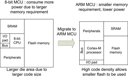
It is a common misunderstanding that 32-bit processor has much larger code size than 8-bit and 16-bit processors. Some people thought that 8-bit processor has 8-bit instructions, 16-bit processors have 16-bit instructions, etc. This is incorrect (Figure 2.8). In reality, many instructions in 8-bit microcontrollers are 16-bit, 24-bits, or other sizes larger than 8-bit, for example, the PIC18 instruction size is 16-bit.
Even for the antiquated 8051 architecture, although some instructions are 1-byte long, many others are 2 or 3 bytes long. The same generally applies to 16-bit architectures, for example, some MSP430 instructions take 6 bytes (or even 8 bytes for the MSP430X).

Most of the instructions in Cortex-M0 and Cortex-M0+ processors are 16 bit, and only a few instructions are 32 bit. Being a load-store architecture (data need to be loaded from memory before being processed, and need to write back to memory after the processing is done), the Cortex-M processor might take more number of instructions, but the overall code size can still be lower due to overall instruction efficiency.
For example, ARM processors support stack operations (PUSH/POP) of multiple registers in a single instruction. This feature is not available in most other architectures. Also, the various address modes also made accessing of local variables, for both signed and unsigned data, very easy (e.g., sign extension for signed data can be done on the fly during a data load). Finally, in 8-bit microcontrollers, integers are still 16-bit and hence each integer data operation requires a sequence of instructions, thus results in much larger code size.
The code density factor has a significant impact to the power consumption because a significant area of the microcontroller chip is occupied by the flash memory (Figure 2.9). For a given application, by moving from an 8-bit processor to ARM Cortex-M processor you could select a chip with much smaller flash memory, possibly by a factor of half the flash size. As a result, you could use a chip with smaller silicon size, possibly a smaller chip package, lower power, and having higher performance at the same time.
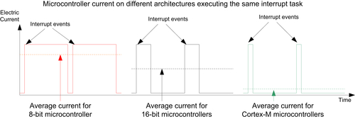
Since the processor is only a small part of the silicon chip, at the system level, you can find that the ARM Cortex-M-based microcontrollers have similar range of active power compare to other 8-bit and 16-bit microcontrollers. And when including the code density and performance factors, it is common to see that the energy efficiency of ARM Cortex-M-based microcontrollers is significantly better than many 8-bit and 16-bit microcontroller products. For example, an interrupt-driven application scenario is shown in Figure 2.10, demonstrating Cortex-M-based microcontrollers can have much lower average power.
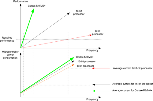
When running other applications that are not interrupt driven, the clock frequency for the Cortex-M0 processor can be reduced significantly compared to 8-bit/16-bit processors to lower the power consumption, as illustrated in Figure 2.11. In this diagram, it is assumed that the Cortex-M0/M0+ microcontroller has slightly higher peak current than 16-bit and 8-bit microcontrollers. In reality, many of the Cortex-M0/Cortex-M0+ microcontrollers have lower peak current than many legacy 8-bit and 16-bit microcontrollers.
Although there are various other 32-bit microcontrollers available with higher performance than the Cortex-M0 and Cortex-M0+ processors, their processor sizes are often significantly larger than the Cortex-M0/M0+ processor. As a result, the average power consumptions of these microcontrollers are higher than the Cortex-M0- and Cortex-M0+-based products.
2.8.3. Other Benefits of ARM Architectures
Often in 8-bit and 16-bit architectures there are a range of limitations. Apart from the obvious data size limitation, address size can also be an issue. For example, many of these architectures cannot handle more than 64 KB memory size, or when over 64 KB memory space is needed, memory banking is needed which results in significant software overhead. Memory banking also increases difficulties in software development. On the other hand, ARM-based microcontrollers use 32-bit addressing, enabling a much larger address space (up to 4 GB, but a small portion of the spaces are assigned to the processor's internal peripherals) and therefore allow easier software development in large projects.
Unlike many 8-bit architecture, the stack of the ARM processors is placed in the main memory address space. Many 8-bit architecture like 8051 requires the stack memory to be placed in specific memory range which have very limited size, which create a severe limitation to the software.
Another limitation of 8-bit microcontroller architectures is the limited instruction sets and fixed register usages for certain instructions. For example, 8051 heavily relies on the accumulator register and data pointer registers to handle data processing and memory transfers. This increases the code size because it needs to keep transferring data into the accumulator and taking it out before and after operations. For instance, when processing integer (16-bt) multiplications on an 8051, a lot of data transfer is required to move data in and out of ACC (Accumulator) register and B register. In Cortex-M processors, the register usages have fewer restrictions.
For applications that require multitasking, the OS support in ARM Cortex-M processor series is also much superior. For example, the banked stack pointers in ARM Cortex-M processors enable efficient context switching and smaller stack size usages.
2.8.4. Software Reusability
For proprietary architectures, quite often program code requires a range of compiler-specific language extensions, which make it difficult to learn and reuse program code. This is not the same in the ARM Cortex-M programming. Since almost everything can be programmed in C/C++ on ARM Cortex-M processors, and there is little dependency on tool chain-specific features, this enables much better software reuse and made learning of programming easier.
..................Content has been hidden....................
You can't read the all page of ebook, please click here login for view all page.