Chapter 4
Architecture
Abstract
This chapter covers the details of the ARMv6-M architecture, the processor architecture on which Cortex®-M0 and Cortex-M0+ processors are based on. The topics included the programmer's model, overview, and features of the memory system, interrupt handling, debug feature, and the start-up sequence of the Cortex-M processors.
Keywords
ARMv6-M architecture; Core's registers; Debug features overview; Exceptions and interrupts; Memory system; Nested Vectored Interrupt Controller (NVIC); Operation modes and states; Programmer's model; Reset sequence; Special registers; Stack memory4.1. Overview of ARMv6-M Architecture
4.1.1. What Architecture Means
The ARM® Cortex®-M0 and Cortex-M0+ Processors are both based on the ARMv6-M architecture. As covered in Section 2.4, the term architecture can refer to the following two areas:
• Architecture: defines how the program execution should behave and how the debuggers interact with the processor
• Microarchitecture: the exact implementation details of the processor, for example, how many pipeline stages, instruction cycles, what type of bus interface used, etc.
Not everything in the ARMv6-M architecture definition is fixed, for example:
• Some of the features defined in the architecture can be optional. For example, the Memory Protection Unit (MPU) is optional and the number of interrupt sources supported in a device can be configured by chip designers.
• Some areas of the architecture can be implementation defined. For example, the number of clock cycle for an instruction to execute is processor design specific. Similarly, a number of identification (ID) registers can be architecturally defined to be needed, but the exact value is processor specific.
• Some of the features on the processor are not essentially architectural features. For example, the single cycle I/O interface on the Cortex-M0+ processor is not a part of the ARMv6-M Architecture specification, but can be very valuable to various applications.
As a result, you can have the Cortex-M0 and Cortex-M0+ processors both based on the ARMv6-M architecture, with different pipeline implementations, and with different feature set. However, when executing a certain program code sequence, you will get the same data processing results, although the timing (i.e., number of clock cycle required) can be different.
4.1.2. Background of the ARMv6-M Architecture
The first ARM processor based on the ARMv6-M architecture is actually a processor called the Cortex-M1 processor. This processor is designed for FPGA applications. The Cortex-M0 processor and then the Cortex-M0+ Processor were developed afterward. There is a little bit of interesting history about this.
After the success of the Cortex-M3 processor in microcontroller applications, ARM had been looking into expanding into FPGA applications. After some investigations, the ARM processor engineering team found that while the Cortex-M3 processor can work fine in FPGA, it is not well optimized for FPGA hardware and therefore the maximum clock frequency is a bit slow. Also, the Cortex-M3 processor has multiple bus interface (based on AHB-Lite protocol) which need to be connected to memory blocks, making it slightly more work for FPGA designers to integrate the processor into their FPGA projects.
When looking into the details of the design requirements, many FPGA applications only need a simple processor for control, and complex data processing could be done in FPGA hardware. On the other hand, the exception handling and system features of the Cortex-M3 processor is very attractive for many FPGA system designers, so ARM decided that there is a need to have a new processor architecture and a new processor based on these requirements.
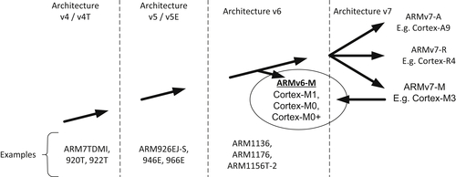
As a result, the ARMv6-M architecture and the Cortex-M1 processor were formed. The programmer's model of the Cortex-M1 processor and the exception model is based on the Cortex-M3 processor, while the instruction set is based on the Thumb instruction set found in ARMv6 architecture, plus additional system instructions required for the Cortex-M processor (e.g., special register accesses), as shown in Figure 4.1.
After the Cortex-M1 processor was developed, a number of ARM customers were very interested to create microcontroller products based on the ARMv6-M architecture. According to my colleagues the idea was formed when some of the microcontroller vendor's management team was chatting with ARM product marketing team in an English pub in an evening—There are a wide range of microcontroller and ASSP/ASIC applications that requires a simple processor with a small instruction set, while still need to have very capable interrupt handling capability. While the Cortex-M1 processor is optimized for FPGA designs, it was not optimized for low-power applications so that it is not suitable for these applications. As a result, ARM decided to design a new processor based on the ARMv6-M architecture, and optimized it for low-power designs and low-cost microcontrollers.
The outcome was the Cortex-M0 processor, and it had become the quickest licensed processor product in ARM history. At a minimum gate count of just 12K gates, it was a ground-breaking product at the time as it enabled many ultra-low power designs to integrate a high performance (related to 8-bit and 16-bit processors) processor, together with sensors, wireless communication chipset, smart analog components, etc.
Over the year, the ARMv6-M architecture expanded further to add additional system features including MPU support (which was not available for Cortex-M0 and Cortex-M1 processors). In addition to the Cortex-M1, Cortex-M0, and Cortex-M0+ processors, the ARMv6-M architecture is also used in SC000, one of the SecurCore® processor products developed for SmartCards and other security products.
4.2. Programmer's Model
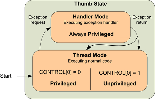
4.2.1. Operation Modes and States
The ARMv6-M architecture has two operation modes and two states. In addition, it can have privileged and unprivileged access levels. These are shown in Figure 4.2. The privileged access level can access to all resources in the processor, while unprivileged access level means some memory regions can be inaccessible, and a few operations cannot be used. Unprivileged access level is not available in the Cortex®-M0 processor, and is optional (device-specific) in the Cortex-M0+ processor.

When the processor is running a program, it is in the Thumb state. In this state, it can be either in the Thread mode or the Handler mode. In the ARMv6-M architecture, the programmer's model of Thread mode and Handler mode are almost completely the same. The only difference is that Thread mode can use a shadowed stack pointer (Figure 4.8) by configuring a special register called CONTROL. Details of stack pointer selection will be covered later in this chapter (Section 4.4).
Architecturally, Thread Mode can be configured as:
• Privileged, or
• Unprivileged (with restriction to certain memory spaces, and cannot access to certain core internal registers). This is defined as an optional feature in the architecture.
In the Cortex-M0+ processor, a program running in privileged state can switch itself into unprivileged access level (if unprivileged level is implemented) by programming the CONTROL register, but cannot switch itself back to privileged state. To get back to privileged state, it must go through an exception sequence. This mechanism prevents an untrusted application task from gaining privileged accesses without going through Operating System (OS) services.
In the Cortex-M0 processor, the processor always executes in privileged state. Unprivileged Thread mode is not available.
The Debug state is active when the processor is halted, for example, by a debugger via a debug connection. This is used for debugging operation only. This state allows the debugger to access or change the processor register values. The debugger can access system memory locations in both Thumb state or Debug state.
When the processor is powered up, it starts with running code in Thumb state and Thread mode, with privileged access level by default.
4.2.2. Registers and Special Registers
In order to perform data processing and controls, a number of registers are required inside the processor core. If data from memory is to be processed, it has to be loaded from the memory to a register in the register bank, processed inside the processor, and then written back to the memory if needed, or kept in the register bank for another operation. This is commonly called “load-store architecture.” By having a sufficient number of registers in the register bank, this mechanism is easy to use, and is C-friendly. It is easy for C compilers to compile a C program into machine code with good performance.
The Cortex-M0 and Cortex-M0+ processor provides a register bank of 16 32-bit registers (most are general purposed, R13–R15 has special purposes), and a number of special registers (Figure 4.3).

The detailed descriptions for these registers are as follows:
R0–R12
Registers R0–R12 are for general uses. Due to the limited space in the 16-bit Thumb® instructions, many of the Thumb instructions can only access R0–R7, which are also called the low registers. While some instructions, like MOV (move), can be used on all registers. When using these registers with ARM® development tools such as the ARM assembler, you can use either upper case (e.g., R0) or lower case (e.g., r0) to specify the register to be used. The initial values of R0–R12 at reset are undefined.
R13, Stack Pointer
R13 is the Stack Pointer. It is used for accessing the stack memory via PUSH and POP operations. There are physically two different stack pointers in Cortex-M0 and Cortex-M0+ Processors.
• The Main Stack Pointer (MSP, or SP_main in ARM documentation) is the default Stack Pointer after reset, and is used when running exception handlers.
• The Process Stack Pointer (PSP, or SP_process in ARM documentation) can only be used in Thread mode (when not handling exceptions).
The stack pointer selection is determined by the CONTROL register, one of the special registers which will be introduced later (CONTROL—Special Register).
When using ARM development tools, you can access the stack pointer using either “R13” or “SP.” Both upper case and lower case (e.g., “r13” or “sp”) can be used. Only one of the stack pointers is visible at a given time. However, you can access to the MSP or PSP directly when using the special register access instructions MRS and MSR. In such cases, the register names “MSP” or “PSP” should be used.
The lowest 2 bits of the stack pointers are always zero and writes to these 2 bits are ignored. In ARM processors, PUSH and POP are always 32-bit accesses because the registers are 32-bit, and the transfers in stack operations must be aligned to a 32-bit word boundary. The initial value of MSP is loaded from the first 32-bit word of the vector table from the program memory during the start-up sequence. The initial value of PSP is undefined.
It is not necessary to use the PSP. In many applications, the system can completely rely on the MSP. The PSP is normally used in designs with an OS, where the stack memory for OS Kernel and the thread-level application codes must be separated.
R14, Link Register
R14 is the Link Register (LR). The LR is used for storing the return address of a subroutine or function call. When BL or BLX is executed, the return address is stored in LR. At the end of the subroutine or function, the return address stored in LR is loaded into the program counter (PC) so that the execution of the calling program can be resumed. In the case where an exception occurs, the LR also provides a special code value which is used by the exception return mechanism. When using ARM development tools, you can access to the LR using either “R14” or “LR.” Both upper and lower case (e.g., “r14” or “lr”) can be used.
Although the return address in the Cortex-M0/M0+ processor is always an even address (bit[0] is zero because smallest instruction are 16-bit and must be half-word aligned), bit zero of LR is readable and writeable. In the ARMv6-M architecture, some instructions require bit zero of a function address set to 1 to indicate Thumb state.
R15, Program Counter
R15 is the PC. It is readable and writeable. A read returns the current instruction address plus four (this is caused by the pipeline nature of the design). Writing to R15 will cause a branch to take place (but unlike a function call, the LR does not get updated).
In the ARM assembler, you can access the PC using either “R15” or “PC,” in either upper or lower case (e.g., “r15” or “pc”). Instruction addresses in the Cortex-M0/M0+ processor must be aligned to half-word address, which means the actual bit zero of the PC should be zero all the time. However, when attempting to carry out a branch using the branch instructions (BX or BLX), the LSB of the PC should be set to1.1 This is to indicate that the branch target is a Thumb program region. Otherwise, it can imply an attempt to switch the processor to ARM state (depending on the instruction used), which is not supported and will cause a fault exception.
xPSR, Combined Program Status Register
The combined Program Status Register (PSR) provides information about program execution and the ALU flags. It consists of the following three PSRs (Figure 4.4):
• Application PSR (APSR),
• Interrupt PSR (IPSR), and
• Execution PSR (EPSR)
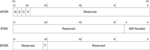
The APSR contains the ALU flags: N (negative flag), Z (zero flag), C (carry or borrow flag), and V (overflow flag). These bits are at the top 4 bits of the APSR. The common use of these flags is to control conditional branches.
The IPSR contains the current executing ISR (Interrupt Service Routine) number. Each exception on the Cortex-M0/M0+ processor has a unique associated ISR number (exception type). This is useful for identifying the current interrupt type during debugging and allows an exception handler that is shared by several exceptions to know which exception it is serving.
The EPSR on the Cortex-M0/M0+ processor contains the T bit which indicates that the processor is in the Thumb state. On the Cortex-M0/M0+ processor, this bit is normally set to 1 because the Cortex-M processors only support Thumb state. If this bit is cleared, a HardFault exception will be generated in the next instruction execution.
These three registers can be accessed as one register called xPSR. For example, when an interrupt takes place, the xPSR is one of the registers that is stored on to the stack memory automatically and restored automatically after returning from an exception. During the stack store and restore, the xPSR is treated as one register (Figure 4.5).

Direct access to the PSRs is only possible through special register access instructions. However, the value of the APSR can affect conditional branches and the carry flag in the APSR can also be used in some data processing instructions.
PRIMASK—Interrupt Mask Special Register
The PRIMASK register is a 1-bit wide interrupt mask register. When set, it blocks all interrupts apart from the Non-Maskable Interrupt (NMI) and the HardFault exception. Effectively it raises the current interrupt priority level to 0 which is the highest value for a programmable exception (Figure 4.6).
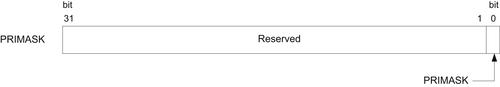
The PRIMASK register can be accessed using special register access instructions (MSR, MRS) as well as using an instruction called CPS. This is commonly used for handling time critical routines.
CONTROL—Special Register
As mentioned earlier, there are two stack pointers in the Cortex-M0 and Cortex-M0+ processors. The stack pointer selection is determined by the processor mode as well as the configuration of the CONTROL register (bit 1—SPSEL). The Thread mode of the Cortex-M0+ processor can either be privileged or unprivileged, and this is also controlled by CONTROL (bit 0—nPRIV) (Figure 4.7).

After reset, the MSP is used, but can be switched to the PSP in Thread mode (when not running an exception handler) by setting bit[1] in the CONTROL register. During running of an exception handler (when the processor is in handler mode), only the MSP is used, and the CONTROL register reads as zero. The bit[1] of CONTROL register can only be changed in Thread mode, or via the exception entrance and return mechanism (Figure 4.8).

Bit[0] of the CONTROL register is for selecting between Privileged and Unprivileged states during Thread mode. Some of the Cortex-M0+ devices and all Cortex-M0 processor-based devices do not support unprivileged state and therefore this bit is always zero (Figure 4.9).
Access of Registers and Special Registers
In C/C++ programming or any other high level languages, the registers in the register bank (R0–R12) can be utilized by the compiler automatically. In most cases, you do not need to worry about which registers being used, unless you are interfacing assembly code and C/C++ code (such mixed language development will be cover in Chapter 21).
The other special registers need to be accessed using some special instructions (MRS and MSR). The CMSIS-CORE provides a number of APIs for such usages. However, please note that some of these special registers cannot be accessed or changed by software (Table 4.1).
4.2.3. Behaviors of the APSR
Data processing instructions can affect destination registers as well as the APSR which is commonly known as ALU status flags in other processor architectures. The APSR is essential for controlling conditional branches. In addition, one of the APSR flags, the C (Carry) bit, can also be used in add and subtract operations.
There are four APSR flags in the Cortex-M0 ad Cortex-M0+ processors (Table 4.2).
Table 4.2
ALU flags on the Cortex®-M0 and Cortex-M0+ processors
| Flag | Descriptions |
| N (bit 31) | Set to bit[31] of the result of the executed instruction. When it is “1,” the result has a negative value (when interpreted as a signed integer). When it is “0,” the result has a positive value or equal zero. |
| Z (bit 30) | Set to “1” if the result of the executed instruction is zero. It can also be set to “1” after a compare instruction is executed if the two values are the same. |
| C (bit 29) | Carry flag of the result. For unsigned addition, this bit is set to “1” if an unsigned overflow occurred. For unsigned subtract operations, this bit is the inverse of the borrow output status. |
| V (bit 28) | Overflow of the result. For signed addition or subtraction, this bit is set to “1” if a signed overflow occurred. |
A few examples of the ALU flag results are as given in Table 4.3.
Table 4.3
| Operation | Results, flags |
| 0x70000000 + 0x70000000 | Result = 0xE0000000, N = 1, Z = 0, C = 0, V = 1 |
| 0x90000000 + 0x90000000 | Result = 0x20000000, N = 0, Z = 0, C = 1, V = 1 |
| 0x80000000 + 0x80000000 | Result = 0x00000000, N = 0, Z = 1, C = 1, V = 1 |
| 0x00001234 − 0x00001000 | Result = 0x00000234, N = 0, Z = 0, C = 1, V = 0 |
| 0x00000004 − 0x00000005 | Result = 0xFFFFFFFF, N = 1, Z = 0, C = 0, V = 0 |
| 0xFFFFFFFF − 0xFFFFFFFC | Result = 0x00000003, N = 0, Z = 0, C = 1, V = 0 |
| 0x80000005 − 0x80000004 | Result = 0x00000001, N = 0, Z = 0, C = 1, V = 0 |
| 0x70000000 − 0xF0000000 | Result = 0x80000000, N = 1, Z = 0, C = 0, V = 1 |
| 0xA0000000 − 0xA0000000 | Result = 0x00000000, N = 0, Z = 1, C = 1, V = 0 |
In the Cortex-M0 and Cortex-M0+ processors, almost all of the data processing instructions modify the APSR; however, some of these instructions do not update the V flag or the C flag. For example, the MULS (multiply) instruction only changes the N flag and the Z flag.
The ALU flags can be used for handling data that is larger than 32-bits. For example, we can perform a 64-bit addition by splitting the operation into two 32-bit additions. The pseudo form of the operation can be written as follows:
    // Calculating Z = X + Y, where X, Y and Z are all 64-bit
    Z[31:0] = X[31:0] + Y[31:0];   // Calculate lower word addition,
                                  // carry flag get updated
Z[63:32] = X[63:32] + Y[63:32] + Carry; // Calculate upper word addition.
An example of carry out such 64-bit add operation in assembly code can be found in Chapter 6 (Section 6.5.1).
The other common usage of APSR flag is to control branching. More on this will be covered in Chapter 5 (Section 5.4.8), where the details of the condition branch instruction will be covered.
4.3. Memory System
4.3.1. Overview
All ARM® Cortex®-M processors have a 4 GB of memory address space. The memory space is architecturally defined into a number of regions, with each region having a recommended usage to help software porting between different devices (Figure 4.10).
The Cortex-M0 and Cortex-M0+ processors contain a number of built-in components like the NVIC (the interrupt controller) and a number of debug components. These are located in fixed memory locations within the system region of the memory map. As a result, all the devices based on the Cortex-M processors have the same programming model for interrupt control and debug. This makes it convenient for software porting as well as helping debug tool vendors to develop debug solutions for the Cortex-M0-based microcontroller or System-on-Chip (SoC) products.

The memory space is shared between instruction memory, data memory, peripherals processor's built-in peripherals (e.g., the interrupt controller), and processor's debug components. However, the debug components are not visible to the software running on the processor (from architecture point of view this is implementation defined, and existing Cortex-M0 and Cortex-M0+ processors are designed to make the debug components to be visible only from debugger). This is different from Cortex-M3, Cortex-M4, and Cortex-M7 processors, where privileged codes can access the debug components.
In most cases, the memories connected to the Cortex-M processors are 32-bits, but it is also possible to connect memory of different data widths to a Cortex-M processor with suitable memory interface hardware. The memory system in Cortex-M processors supports memory transfers of different sizes such as byte (8-bit), half word (16-bit), and word (32-bit). The Cortex-M0 and Cortex-M0+ processor designs can be configured to support either little endian or big endian memory systems, but cannot switch from one to another in an implemented design.
Since the memory system and peripherals connected to the Cortex-M0 or Cortex-M0+ processors are developed by microcontroller vendors or SoC designers, different memory sizes and memory types can be found in different Cortex-M0/M0+-based products.
4.3.2. Single Cycle I/O Interface
The Cortex-M0+ Processor has an optional feature, which allows chip designer to add a separated bus interface (in addition to the main system bus), which allows certain peripheral registers to be accessed in a single clock cycle. This enables the microcontroller product to provide better performance in I/O operations, as well as improve energy efficiency in I/O intensive applications.
When this feature is implemented, the address space connect to the single cycle I/O interface appears as a part of the main memory space, so from software point of view the peripheral registers in the single cycle I/O bus works in the same way as registers on the AHB-Lite system bus. However, this interface can only be used for data accesses and does not support instruction accesses (Figure 4.11).

The single cycle I/O interface is intended for connecting small number of peripherals, which need faster access speed (e.g., GPIO). Peripherals like UART and timers are normally connected via the AHB-Lite system bus because the associated operations typically do not have short-latency requirement and do not occur frequently.
4.3.3. Memory Protection Unit
Another optional feature in the Cortex-M0+ processor is the MPU (MPU). This is a programmable unit and is to be used with the privileged–unprivileged states of the processor. The MPU provides up to eight programmable regions, and each region can be defined with different starting addresses, sizes, and memory access permissions.
In a multitasking system, an OS can run some of the application tasks in unprivileged state and the OS can program the optional MPU each time it switches between tasks, so each of the unprivileged application tasks run in their own permitted memory space and can only access to memory locations allocated to them.
The configuration registers of the MPU is privileged access only so that an unprivileged task cannot change the access permission to bypass the MPU.
More information about the MPU is covered in Chapter 12.
4.4. Stack Memory Operations
Stack memory is a memory usage mechanism that allows the system memory to be used as temporary data storage that behaves as a first-in-last-out buffer. One of the essential elements of stack memory operation is a register called the Stack Pointer. The stack pointer indicates where the current stack memory location is, and is adjusted automatically each time a stack operation is carried out.
In the Cortex®-M processors, the Stack Pointer is register R13 in the register bank. Physically there are two stack pointers in the Cortex-M processors, but only one of them is used at a time, depending on the current value of the CONTROL register and the state of the processor (see Figure 4.8).
In common terms, storing data to the stack is called pushing (using the PUSH instruction) and restoring data from the stack is called popping (using the POP instruction). Depending on processor architecture, some processors perform storing of new data to stack memory using incremental address indexing and some use decrement address indexing. In the Cortex-M processors, the stack operation is based on a “full-descending” stack model. This means the stack pointer always points to the last filled data in the stack memory, and the stack pointer predecrements for each new data store (PUSH) (Figure 4.12).
PUSH and POP are commonly used at the beginning and at the end of a function or subroutine. At the beginning of a function, the current contents of the registers used by the calling program are stored onto the stack memory using PUSH operations, and at the end of the function, the data on the stack memory is restored to the registers using POP operations. Typically, each register PUSH operation should have a corresponding register POP operation; otherwise the stack pointer will not be able to restore registers to their original values. This can result in unpredictable behaviors, for example, function return to incorrect addresses.
The minimum data size to be transferred for each push and pop operations is one word (32-bit) and multiple registers can be pushed or popped in one instruction. The stack memory accesses in the Cortex-M processors are designed to be always word aligned (address values must be a multiple of 4, for example, 0x0, 0x4, 0x8,…) as this gives the best efficiency for minimum design complexity. For this reason, bit [1:0] of both stack pointers in the Cortex-M processors are hardwired to zeros and read as zeros.

In programming, the stack pointer can be accessed as either R13 or SP in the program codes. Depending on the processor state and the CONTROL register value, the stack pointer accessed can either be the MSP or the PSP. In many simple applications, only one stack pointer is needed and by default the MSP is used. The PSP is usually only required when an OS is used in the embedded application.
In a typical embedded application with an OS, the OS kernel uses the MSP and the application processes use the PSP. This allows the stack for the kernel to be separate from stack memory for the application processes. This allows the OS to carry out context switching quickly (switching from execution of one application process to another). Also, since exception handlers only use main stack, each of the stack spaces allocated to application tasks do not need to reserve space needed for exception handler, thus allow better memory usage efficiency.
Even though the OS kernel only uses the MSP as its stack pointer, it can still access the value in PSP by using special register access instructions (MRS and MSR) (Table 4.4).
Since the stack grows downward (full-descending), it is common for the initial value of the stack pointer to be set to the upper boundary of SRAM. For example, if the SRAM memory range is from 0x20000000 to 0x20007FFF, we can start the stack pointer at 0x20008000. In this case, the first stack PUSH will take place at address 0x20007FFC, the top word of the SRAM (see Figure 4.13).
Table 4.4
Stack pointer usage definition
| Processor state | CONTROL[1] = 0 (default setting) | CONTROL[1] = 1 (OS has started) |
| Thread mode | Use MSP (R13 is MSP) | Use PSP (R13 is PSP) |
| Handler mode | Use MSP (R13 is MSP) | Use MSP (R13 is MSP) |

The initial value of MSP is stored at the beginning of the program memory. Here we will find the exception vector table, which is introduced in the next section. The initial value of PSP is undefined, and therefore the PSP must be initialized by software before using it.
In many software development environments, the stack pointer can be set up again during the C start-up code (before entering “main()”). This two-stage stack initialization sequence enables a system to boot up the system with the stack pointing to a small internal SRAM inside the chip, and then change the stack definition to a larger external memory space after the external memory controller has been initialized.
4.5. Exceptions and Interrupts
Exceptions are events that cause changes to program control: when an exception occurred, instead of continuing program execution, the processor suspends the current executing task and executes a part of the program code called the exception handler. After the exception handler is completed, it will then resume the normal program execution.
There are various types of exceptions, and interrupts are a subset of exceptions. The Cortex®-M0 and Cortex-M0+ processors supports up to 32 external interrupts (commonly referred as IRQ), and an additional special interrupt called the NMI (Non-Maskable Interrupt). The exception handlers for interrupt events are commonly known as ISRs (Interrupt Service Routines). Interrupts are usually generated by on-chip peripherals, or by external input through I/O ports. The exact number of available interrupts on the Cortex-M0/M0+ processor depends on the microcontroller product you use. In systems with more peripherals, it is possible for multiple interrupt sources to share one interrupt connection.
In addition to the NMI and IRQs, there are a number of system exceptions in the Cortex-M0/M0+ processors primarily for OS use and fault handling, which are as given in Table 4.5.
Table 4.5
| Exception type | Exception number | Description |
| Reset | 1 | Power on reset or system reset. |
| NMI | 2 | Non-Maskable interrupt—highest priority exception that cannot be disabled. For safety critical events. |
| HardFault | 3 | For fault handling—activated when a system error is detected. |
| SVCall | 11 | Supervisor call—activated when SVC instruction is executed. Primarily for OS applications. |
| PendSV | 14 | Pendable service (system) call—activate by writing to an interrupt control and status register. Primarily for OS applications. |
| SysTick | 15 | System Tick timer exception – typically used by an OS for a regular system tick exception. The system tick timer (SysTick) is an optionala timer unit inside the Cortex®-M processor. |
| IRQ0 to IRQ31b | 16–47 | Interrupts—can be from external sources or from on-chip peripherals. |
Each exception has an exception number. This number is reflected in various registers including the IPSR, and is used to define the exception vector addresses. Note that exception number is separated from interrupt numbers used in device driver libraries. In most device driver libraries, system exceptions are defined using negative numbers, and interrupts are defined as positive numbers from 0 to 31.
Reset is a special type of exception. When the Cortex-M0/M0+ processor exits from a reset, it executes the reset handler in thread mode (no need to return from handler to thread). Also, the exception number of 1 is not visible in the IPSR.
Apart from NMI, HardFault and reset, all other exceptions have a programmable priority level. The priority level for NMI and HardFault are fixed and both have a higher priority than the rest of the exceptions. More details will be covered in Chapter 8 of this book.
4.6. Nested Vectored Interrupt Controller
In order to prioritize the interrupt requests and handle other exceptions, the Cortex®-M processors have a built-in interrupt controller called the NVIC. The interrupt management function is controlled by a number of programmable registers in the NVIC. These registers are memory mapped, with the addresses located within the System Control Space (SCS) as illustrated in Figure 4.10.
The NVIC supports a number of features:
• Flexible interrupt management
• Nested interrupt support
• Vectored exception entry
• Interrupt masking
4.6.1. Flexible Interrupt Management
In the Cortex-M processors, each external interrupt can be enabled, disabled, and can have its pending status set or clear by software. It can also accept exception requests at signal level (interrupt request from a peripheral remain asserted until the ISR clears the interrupt request), as well as an exception request pulse (minimum 1 clock cycle). This allows the interrupt controller to be used with any interrupt source.
4.6.2. Nested Interrupt Support
In the Cortex-M processors, each exception has a priority level. The priority level can be fixed or programmable (all interrupts has programmable priority levels). When an exception occurs such as an external interrupt, the NVIC will compare the priority of this exception to the current level. If the new exception has a higher priority, the current running task will be suspended. Some of the registers will be stored on to the stack memory and the processor will start executing the exception handler of the new exception. This process is called “preemption.” When the higher priority exception handler is completes, it is terminated with an exception return operation and the processor automatically restores the registers from the stack and resumes the task that was running previously. This mechanism allows nesting of exception services without any software overhead.
4.6.3. Vectored Exception Entry
When an exception occurs, the processor will need to locate the starting point of the corresponding exception handler. Traditionally, in ARM® processors such as the ARM7TDMI, this is done by software. The Cortex-M processors automatically locate the starting point of the exception handler from a vector table in the memory. As a result, the delay from the occurrence of the exception to the execution of the exception handlers is reduced.
4.6.4. Interrupt Masking
The NVIC in the Cortex-M processors provides an interrupt masking feature via the PRIMASK special register. This can disable all exceptions except HardFault and NMI. This masking is useful for operations that should not be interrupted such as time critical control tasks or real time multimedia codecs. (Note: Processors based on ARMv7-M have additional interrupt masking registers, see Section 22.5 in Chapter 22.)
These NVIC features help makes the Cortex-M processors easier to use, provides better response times and reduces program code size by managing the exceptions in the NVIC hardware.
4.7. System Control Block
Apart from the NVIC, the SCS also contains a number of other registers for system management. This is called the System Control Block. It contains registers for sleep mode features, system exception configurations as well as a register containing the processor identification code (which can be used by in circuit debuggers for detection of the processor type).
4.8. Debug System
Although being currently the smallest processors in the ARM® processor family, the Cortex®-M0 and Cortex-M0+ processors support a range of debug features. The processor core provides halt mode debug, stepping, register accesses, and memory accesses for debugger, and additional debug blocks provide debug features like the Breakpoint Unit (BPU) and Data Watchpoint (DWT) units. The BPU supports up to four hardware breakpoints, and the DWT supports up to two watchpoints.
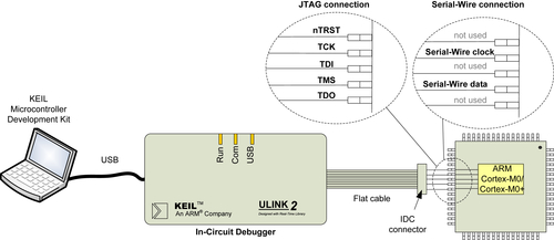
In order to allow a debugger to control the aforementioned debug components and carry out debug operations, the Cortex-M processors provide a debug interface unit. This debug interface unit can either use the JTAG protocol or the Serial Wire Debug (SWD) protocol (Figure 4.14). In some Cortex-M-based products, the microcontroller vendors can also choose to use a debug interface unit which supports both JTAG and SWD protocol. However, typical Cortex-M0 and Cortex-M0+ implementations are likely to support only one protocol with SWD probably being preferred due to fewer pins required.
The SWD protocol is a new standard developed by ARM® and can reduce the number debug connection pins to just two signals. It can handle all the same debug features as JTAG without any loss of performance. The SWD interface shares the same connector as JTAG: the Serial clock signal is shared with JTAG TCK signal, and the Serial Wire data is shared with the JTAG TMS signal. There are many debug emulators for ARM microcontrollers including ULINK2 (from Keil®), and JLink (from SEGGER) that support the SWD protocol.
4.9. Program Image and Start-up Sequence
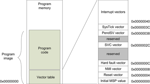
To understand the start-up sequence of the Cortex®-M processors, we need to have a quick overview on the program image first. Normally, the program image for the Cortex-M0/M0+ processor is located from address 0x00000000.
The beginning of the program image contains the vector table. It contains the starting addresses (vectors) of exceptions. Each vector is located in address of “Exception_Number x 4.” For example, external IRQ #0 is exception type #16, therefore the address of the vector for IRQ#0 is in 16x4 = 0x40. These vectors have LSB set to 1 to indicate that the exceptions handlers are to be executed with Thumb instructions. The size of the vector table depends on how many interrupts are implemented.
The vector table also defines the initial value of the MSP. This is stored in the first word of the vector table, as shown in Figure 4.15.
When the processor exits from reset, it will first read the first two word addresses in the vector table, as shown in Figure 4.16. The first word is the initial MSP value, and the second word is the reset vector which determines the starting of the program execution address (reset handler).
For example, if we have boot code starting from address 0x000000C0, we need to put this address value in the reset vector location with the LSB set to one to indicate that it is Thumb code. Therefore, the value in address 0x00000004 is set to 0x000000C1, as shown in Figure 4.17. After the reset vector is fetched by the processor, it will start executing program code from the address found there. This behavior is different from traditional ARM® processors (e.g., ARM7TDMI), where the processor executes the program starting from address 0x00000000, and the vectors in the vector table are instructions as opposed to address values in the Cortex-M processors.

The reset sequence also initializes the MSP. Assume we have SRAM located from 0x20000000 to 0x20007FFF, and we want to put the main stack at the top of the SRAM, we can set this up by putting 0x20008000 in address 0x00000000 (also shown in Figure 4.17).
Since the Cortex-M processor will first decrement the stack pointer before pushing the data on to the stack, the first stacked item will be located in 0x200007FFC, which is just at the top of the SRAM. While the second stacked item will be in 0x20007FF8, below the first stacked item.
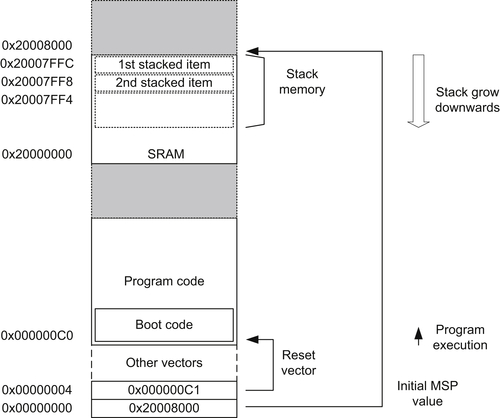
This behavior is different from traditional ARM processors and many other microcontroller architectures where the stack pointer has to be initialized by software code rather than a value in a fixed address.
If the PSP is to be used, it must be initialized by software code before writing to the CONTROL register to switch the stack pointer. The reset sequence only initializes the MSP and not the PSP.
Different software development tools have different ways of specifying the initial stack pointer value and the values for the reset and exception vectors. Most of the development tools come with code examples demonstrating how this can be done with their development flow. In most compilation tools, the vector table can be defined completely using C codes.
..................Content has been hidden....................
You can't read the all page of ebook, please click here login for view all page.