Memory Protection Unit
Abstract
This chapter introduces the Memory Protection Unit (MPU), an optional programmable unit in the Cortex®-M0+ processor, including its usages, the programmer's model, the configuration steps, and the differences between the MPU in ARMv6-M and ARMv7-M processors.
Keywords
Comparison of MPU with ARMv7-M architecture; Memory barrier; Memory protection unit (MPU) overview; MPU configuration; MPU registers; MPU usages; Sub-Region Disable12.1. What is MPU?
12.2. MPU Use Cases
12.3. Technical Introduction
12.4. MPU Registers
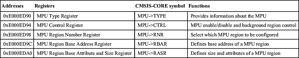
Table 12.1
| Addresses | Registers | CMSIS-CORE symbol | Functions |
| 0xE000ED90 | MPU Type Register | MPU->TYPE | Provides information about the MPU |
| 0xE000ED94 | MPU Control Register | MPU->CTRL | MPU enable/disable and background region control |
| 0xE000ED98 | MPU Region Number Register | MPU->RNR | Select which MPU region to be configured |
| 0xE000ED9C | MPU Region Base Address Register | MPU->RBAR | Defines base address of a MPU region |
| 0xE000EDA0 | MPU Region Base Attribute and Size Register | MPU->RASR | Defines size and attributes of a MPU region |
12.4.1. MPU Type Register
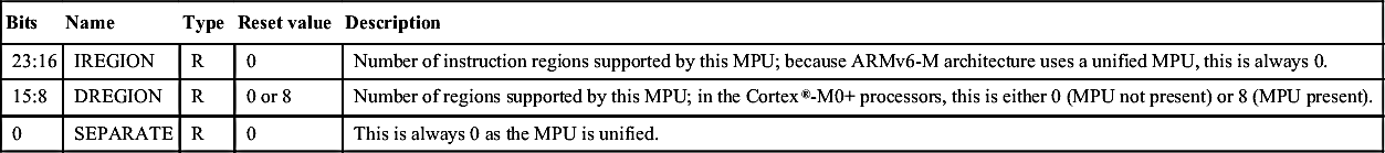
Table 12.2
MPU Type Register (MPU->TYPE, 0xE000ED90)
| Bits | Name | Type | Reset value | Description |
| 23:16 | IREGION | R | 0 | Number of instruction regions supported by this MPU; because ARMv6-M architecture uses a unified MPU, this is always 0. |
| 15:8 | DREGION | R | 0 or 8 | Number of regions supported by this MPU; in the Cortex®-M0+ processors, this is either 0 (MPU not present) or 8 (MPU present). |
| 0 | SEPARATE | R | 0 | This is always 0 as the MPU is unified. |
12.4.2. MPU Control Register
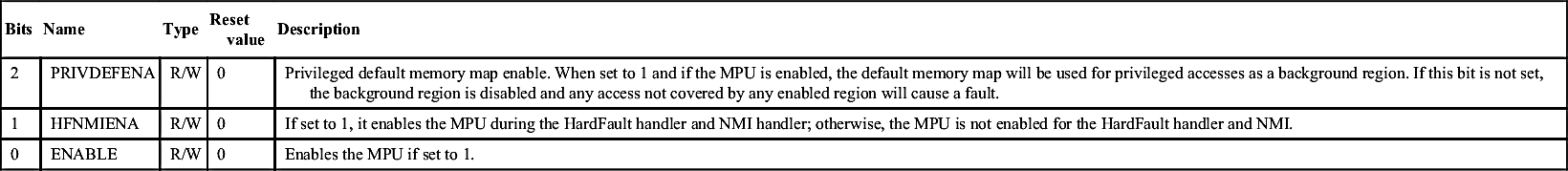
Table 12.3
MPU Control Register (MPU->CTRL, 0xE000ED94)
| Bits | Name | Type | Reset value | Description |
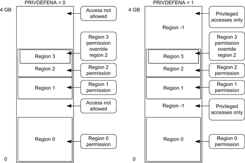
| 2 | PRIVDEFENA | R/W | 0 | Privileged default memory map enable. When set to 1 and if the MPU is enabled, the default memory map will be used for privileged accesses as a background region. If this bit is not set, the background region is disabled and any access not covered by any enabled region will cause a fault. |
| 1 | HFNMIENA | R/W | 0 | If set to 1, it enables the MPU during the HardFault handler and NMI handler; otherwise, the MPU is not enabled for the HardFault handler and NMI. |
| 0 | ENABLE | R/W | 0 | Enables the MPU if set to 1. |
12.4.3. MPU Region Number Register

12.4.4. MPU Region Base Address Register
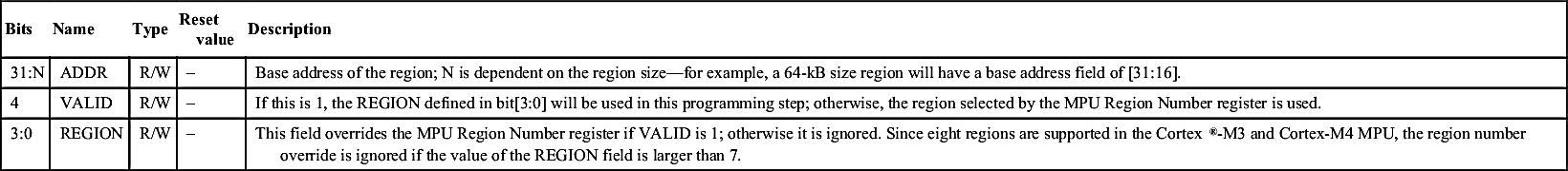
Table 12.5
MPU Region Base Address Register (MPU->RBAR, 0xE000ED9C)
| Bits | Name | Type | Reset value | Description |
| 31:N | ADDR | R/W | – | Base address of the region; N is dependent on the region size—for example, a 64-kB size region will have a base address field of [31:16]. |
| 4 | VALID | R/W | – | If this is 1, the REGION defined in bit[3:0] will be used in this programming step; otherwise, the region selected by the MPU Region Number register is used. |
| 3:0 | REGION | R/W | – | This field overrides the MPU Region Number register if VALID is 1; otherwise it is ignored. Since eight regions are supported in the Cortex®-M3 and Cortex-M4 MPU, the region number override is ignored if the value of the REGION field is larger than 7. |
12.4.5. MPU Region Base Attribute and Size Register
Table 12.6
MPU Region Base Attribute and Size Register (MPU->RASR, 0xE000EDA0)
| Bits | Name | Type | Reset value | Description |
| 31:29 | Reserved | – | – | – |
| 28 | XN | R/W | – | Instruction Access Disable (1 = Disable instruction fetch from this region; an attempt to do so will result in a memory management fault) |
| 27 | Reserved | – | – | – |
| 26:24 | AP | R/W | – | Data Access Permission field |
| 23:22 | Reserved | – | – | – |
| 21:19 | TEX | R/W | – | Type Extension field—always 0 in ARMv6-M |
| 18 | S | R/W | – | Shareable |
| 17 | C | R/W | – | Cacheable |
| 16 | B | R/W | – | Bufferable |
| 15:8 | SRD | R/W | – | Sub-Region Disable |
| 7:6 | Reserved | – | – | |
| 5:1 | REGION SIZE | R/W | – | MPU Protection Region size |
| 0 | ENABLE | R/W | – | Region enable |

Table 12.7
Encoding of REGION SIZE field for different memory region sizes
| REGION size | Size | REGION size | Size |
| b00000 | Reserved | b10000 | 128 KB |
| b00001 | Reserved | b10001 | 256 KB |
| b00010 | Reserved | b10010 | 512 KB |
| b00011 | Reserved | b10011 | 1 MB |
| b00100 | Reserved | b10100 | 2 MB |
| b00101 | Reserved | b10101 | 4 MB |
| b00110 | Reserved | b10110 | 8 MB |
| b00111 | 256 byte | b10111 | 16 MB |
| b01000 | 512 byte | b11000 | 32 MB |
| b01001 | 1 KB | b11001 | 64 MB |
| b01010 | 2 KB | b11010 | 128 MB |
| b01011 | 4 KB | b11011 | 256 MB |
| b01100 | 8 KB | b11100 | 512 MB |
| b01101 | 16 KB | b11101 | 1 GB |
| b01110 | 32 KB | b11110 | 2 GB |
| b01111 | 64 KB | b11111 | 4 GB |
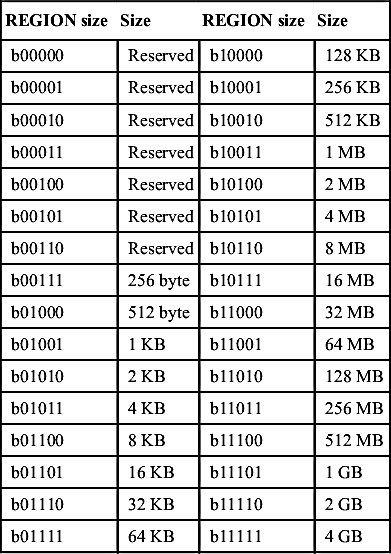
Table 12.8
Encoding of AP field for various access permission configurations
| AP Value | Privileged access | User access | Description |
| 000 | No access | No access | No access |
| 001 | Read/Write | No access | Privileged access only |
| 010 | Read/Write | Read only | Write in a user program generates a fault |
| 011 | Read/Write | Read/Write | Full access |
| 100 | Unpredictable | Unpredictable | Unpredictable |
| 101 | Read only | No access | Privileged read only |
| 110 | Read only | Read only | Read only |
| 111 | Read only | Read only | Read only |
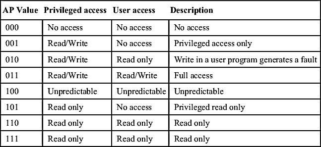
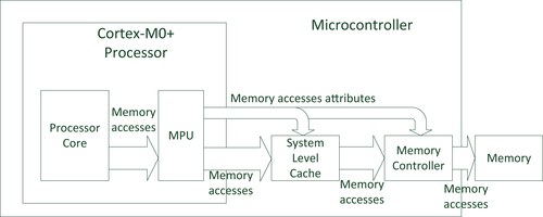
Table 12.9
Memory attributes (TEX is always 0 in ARMv6-M architecture)
| TEX | C | B | Description | Region shareability |
| b000 | 0 | 0 | Strongly ordered (transfers carry out and complete in programmed order) | Shareable |
| b000 | 0 | 1 | Shared device (write can be buffered) | Shareable |
| b000 | 1 | 0 | Outer and inner write-through; no write allocate | [S] |
| b000 | 1 | 1 | Outer and inner write-back; no write allocate | [S] |
| b001 | 0 | 0 | Outer and inner non-cacheable (not supported) | [S] |
| b001 | 0 | 1 | Reserved | Reserved |
| b001 | 1 | 0 | Implementation defined (not supported) | – |
| b001 | 1 | 1 | Outer and inner write-back; write and read allocate (not supported) | [S] |
| b010 | 0 | 0 | Nonshared device (not supported) | Not shared |
| b010 | 0 | 1 | Reserved | Reserved |
| b010 | 1 | X | Reserved | Reserved |
| b1BB | A | A | Cached memory; BB = outer policy, AA = inner policy (not supported) | [S] |

Table 12.10
Commonly used memory attributes in microcontrollers
| Type | Memory type | Commonly used memory attributes |
| ROM, flash (program memories) | Normal memory | Nonshareable, write-through C = 1, B = 0, TEX = 0, S = 0 |
| Internal SRAM | Normal memory | Shareable, write-through C = 1, B = 0, TEX = 0, S = 1/S = 0 |
| External RAM | Normal memory | Shareable, write-back C = 1, B = 1, TEX = 0, S = 1/S = 0 |
| Peripherals | Device | Shareable devices C = 0, B = 1, TEX = 0, S = 1/S = 0 |
12.5. Setting Up the MPU

#define MPU_DEFS_RASR_SIZE_256B  (0x07 << MPU_RASR_SIZE_Pos)
#define MPU_DEFS_RASR_SIZE_512B  (0x08 << MPU_RASR_SIZE_Pos)
#define MPU_DEFS_RASR_SIZE_1KB   (0x09 << MPU_RASR_SIZE_Pos)
#define MPU_DEFS_RASR_SIZE_2KB   (0x0A << MPU_RASR_SIZE_Pos)
#define MPU_DEFS_RASR_SIZE_4KB   (0x0B << MPU_RASR_SIZE_Pos)
#define MPU_DEFS_RASR_SIZE_8KB   (0x0C << MPU_RASR_SIZE_Pos)
#define MPU_DEFS_RASR_SIZE_16KB  (0x0D << MPU_RASR_SIZE_Pos)
#define MPU_DEFS_RASR_SIZE_32KB  (0x0E << MPU_RASR_SIZE_Pos)
#define MPU_DEFS_RASR_SIZE_64KB  (0x0F << MPU_RASR_SIZE_Pos)
#define MPU_DEFS_RASR_SIZE_128KB (0x10 << MPU_RASR_SIZE_Pos)
#define MPU_DEFS_RASR_SIZE_256KB (0x11 << MPU_RASR_SIZE_Pos)
#define MPU_DEFS_RASR_SIZE_512KB (0x12 << MPU_RASR_SIZE_Pos)
#define MPU_DEFS_RASR_SIZE_1MB   (0x13 << MPU_RASR_SIZE_Pos)
#define MPU_DEFS_RASR_SIZE_2MB   (0x14 << MPU_RASR_SIZE_Pos)
#define MPU_DEFS_RASR_SIZE_4MB   (0x15 << MPU_RASR_SIZE_Pos)
#define MPU_DEFS_RASR_SIZE_8MB   (0x16 << MPU_RASR_SIZE_Pos)
#define MPU_DEFS_RASR_SIZE_16MB  (0x17 << MPU_RASR_SIZE_Pos)
#define MPU_DEFS_RASR_SIZE_32MB  (0x18 << MPU_RASR_SIZE_Pos)
#define MPU_DEFS_RASR_SIZE_64MB  (0x19 << MPU_RASR_SIZE_Pos)
#define MPU_DEFS_RASR_SIZE_128MB (0x1A << MPU_RASR_SIZE_Pos)
#define MPU_DEFS_RASR_SIZE_256MB (0x1B << MPU_RASR_SIZE_Pos)
#define MPU_DEFS_RASR_SIZE_512MB (0x1C << MPU_RASR_SIZE_Pos)
#define MPU_DEFS_RASR_SIZE_1GB   (0x1D << MPU_RASR_SIZE_Pos)
#define MPU_DEFS_RASR_SIZE_2GB   (0x1E << MPU_RASR_SIZE_Pos)
#define MPU_DEFS_RASR_SIZE_4GB   (0x1F << MPU_RASR_SIZE_Pos)
#define MPU_DEFS_RASE_AP_NO_ACCESS       (0x0 << MPU_RASR_AP_Pos)
#define MPU_DEFS_RASE_AP_PRIV_RW         (0x1 << MPU_RASR_AP_Pos)
#define MPU_DEFS_RASE_AP_PRIV_RW_USER_RO (0x2 << MPU_RASR_AP_Pos)
#define MPU_DEFS_RASE_AP_FULL_ACCESS     (0x3 << MPU_RASR_AP_Pos)
#define MPU_DEFS_RASE_AP_PRIV_RO         (0x5 << MPU_RASR_AP_Pos)
#define MPU_DEFS_RASE_AP_RO              (0x6 << MPU_RASR_AP_Pos)
#define MPU_DEFS_NORMAL_MEMORY_WT        (MPU_RASR_C_Msk)
#define MPU_DEFS_NORMAL_MEMORY_WB        (MPU_RASR_C_Msk | MPU_RASR_B_Msk)
#define MPU_DEFS_NORMAL_SHARED_MEMORY_WT (MPU_RASR_C_Msk | MPU_RASR_S_Msk)
#define MPU_DEFS_NORMAL_SHARED_MEMORY_WB (MPU_DEFS_NORMAL_MEMORY_WB | MPU_RASR_S_Msk)
#define MPU_DEFS_SHARED_DEVICE           (MPU_RASR_B_Msk)
#define MPU_DEFS_STRONGLY_ORDERED_DEVICE (0x0)
// -------------------------------------------------------------------------
int mpu_setup(void)
{
  uint32_t i;
  uint32_t const mpu_cfg_rbar[4] = {
      0x08000000,            // Flash address for STM32L0
      0x20000000,     // SRAM
      IOPPERIPH_BASE, // GPIO base address
      USART1_BASE     // USART base address
   };
  uint32_t const mpu_cfg_rasr[4] = {
     (MPU_DEFS_RASR_SIZE_64KB     | MPU_DEFS_NORMAL_MEMORY_WT   |
       MPU_DEFS_RASE_AP_FULL_ACCESS | MPU_RASR_ENABLE_Msk),  //  Flash
     (MPU_DEFS_RASR_SIZE_8KB     | MPU_DEFS_NORMAL_MEMORY_WT   |
       MPU_DEFS_RASE_AP_FULL_ACCESS | MPU_RASR_ENABLE_Msk),  //  SRAM
     (MPU_DEFS_RASR_SIZE_4KB     | MPU_DEFS_SHARED_DEVICE         |
   MPU_DEFS_RASE_AP_FULL_ACCESS | MPU_RASR_ENABLE_Msk),  //  GPIO A to GPIO D
     (MPU_DEFS_RASR_SIZE_2KB     | MPU_DEFS_SHARED_DEVICE         |
   MPU_DEFS_RASE_AP_FULL_ACCESS | MPU_RASR_ENABLE_Msk)    //  USART
  };
  if (MPU->TYPE==0) {return 1;}    // NO MPU: Return 1 to indicate error
  __DMB();                         // Make sure outstanding transfers are done
  MPU->CTRL = 0;                   // Disable the MPU
  for (i=0;i<4;i++) {              // Configure only 4 regions
    MPU->RNR  = i;                 // Select which MPU region to configure
    MPU->RBAR = mpu_cfg_rbar[i];   // Configure region base address register
    MPU->RASR = mpu_cfg_rasr[i];   // Configure region attribute and size register
    }
  for (i=4;i<8;i++) {// Disabled unused regions
    MPU->RNR  = i;   // Select which MPU region to configure
    MPU->RBAR = 0;   // Configure region base address register
    MPU->RASR = 0;   // Configure region attribute and size register
    }
  MPU->CTRL = MPU_CTRL_ENABLE_Msk; // Enable the MPU
  __DSB();  // Memory barriers to ensure subsequence data & instruction
  __ISB();  //  transfers using updated MPU settings
  return 0; // No error
}
// -------------------------------------------------------------------------

// -------------------------------------------------------------------------
int mpu_setup(void)
{
  uint32_t i;
  uint32_t const mpu_cfg_rbar[4] = {
    // Flash address for STM32L0
    (0x08000000| MPU_RBAR_VALID_Msk     | (MPU_RBAR_REGION_Msk & 0)),
    // SRAM
    (0x20000000| MPU_RBAR_VALID_Msk     | (MPU_RBAR_REGION_Msk & 1)),
    // GPIO base address
    (IOPPERIPH_BASE| MPU_RBAR_VALID_Msk | (MPU_RBAR_REGION_Msk & 2)),
    // USART base address
    (USART1_BASE| MPU_RBAR_VALID_Msk    | (MPU_RBAR_REGION_Msk & 3))
    };
  uint32_t const mpu_cfg_rasr[4] = {
    (MPU_DEFS_RASR_SIZE_64KB      | MPU_DEFS_NORMAL_MEMORY_WT |
     MPU_DEFS_RASE_AP_FULL_ACCESS | MPU_RASR_ENABLE_Msk), // Flash
    (MPU_DEFS_RASR_SIZE_8KB       | MPU_DEFS_NORMAL_MEMORY_WT |
     MPU_DEFS_RASE_AP_FULL_ACCESS | MPU_RASR_ENABLE_Msk), // SRAM
    (MPU_DEFS_RASR_SIZE_4KB       | MPU_DEFS_SHARED_DEVICE    |
     MPU_DEFS_RASE_AP_FULL_ACCESS | MPU_RASR_ENABLE_Msk), // GPIO A to GPIO D
    (MPU_DEFS_RASR_SIZE_2KB       | MPU_DEFS_SHARED_DEVICE    |
     MPU_DEFS_RASE_AP_FULL_ACCESS | MPU_RASR_ENABLE_Msk)  // USART
    };
  if (MPU->TYPE==0) {return 1;}    // Return 1 to indicate error
  __DMB();                         // Make sure outstanding transfers are done
  MPU->CTRL = 0;                   // Disable the MPU
  for (i=0;i<4;i++) {              // Configure only 4 regions
    MPU->RBAR = mpu_cfg_rbar[i];   // Configure region base address register
    MPU->RASR = mpu_cfg_rasr[i];   // Configure region attribute and size register
    }
  for (i=4;i<8;i++) {// Disabled unused regions
    MPU->RNR  = i;   // Select which MPU region to configure
    MPU->RBAR = 0;   // Configure region base address register
    MPU->RASR = 0;   // Configure region attribute and size register
    }
  MPU->CTRL = MPU_CTRL_ENABLE_Msk; // Enable the MPU
  __DSB();  // Memory barriers to ensure subsequence data & instruction
  __ISB();  //  transfers using updated MPU settings
  return 0; // No error
}
// -------------------------------------------------------------------------
// -------------------------------------------------------------------------
// Enable MPU with input options
// Options can be MPU_CTRL_HFNMIENA_Msk or MPU_CTRL_PRIVDEFENA_Msk
void mpu_enable(uint32_t options)
{
  MPU->CTRL = MPU_CTRL_ENABLE_Msk | options;   // Disable the MPU
  __DSB();  // Ensure MPU settings take effects
  __ISB();  // Sequence instruction fetches using update settings
  return;
}
// Disable the MPU.
void mpu_disable(void)
{
  __DMB();       // Make sure outstanding transfers are done
  MPU->CTRL = 0; // Disable the MPU
  return;
}
// Function to disable a region (0 to 7)
void mpu_region_disable(uint32_t region_num)
{
  MPU->RNR  = region_num;
  MPU->RBAR = 0;
  MPU->RASR = 0;
  return;
}
// Function to enable a region
void mpu_region_config(uint32_t region_num, uint32_t addr, uint32_t size, uint32_t attributes)
{
  MPU->RNR  = region_num;
  MPU->RBAR = addr;
  MPU->RASR = size | attributes;
  return;
}
int mpu_setup(void)
{
  if (MPU->TYPE==0) {return 1;}    // NO MPU: Return 1 to indicate error
  mpu_disable();
  mpu_region_config(0, 0x08000000, MPU_DEFS_RASR_SIZE_64KB,
    MPU_DEFS_NORMAL_MEMORY_WT | MPU_DEFS_RASE_AP_FULL_ACCESS  |
    MPU_RASR_ENABLE_Msk), // Region 0 - Flash
  mpu_region_config(1, 0x20000000, MPU_DEFS_RASR_SIZE_8KB,
    MPU_DEFS_NORMAL_MEMORY_WT | MPU_DEFS_RASE_AP_FULL_ACCESS  |
    MPU_RASR_ENABLE_Msk), // Region 1 - SRAM
  mpu_region_config(2, IOPPERIPH_BASE, MPU_DEFS_RASR_SIZE_4KB,
    MPU_DEFS_SHARED_DEVICE    | MPU_DEFS_RASE_AP_FULL_ACCESS  |
    MPU_RASR_ENABLE_Msk), // Region 2 - GPIO A to GPIO D
  mpu_region_config(3, USART1_BASE, MPU_DEFS_RASR_SIZE_2KB,
    MPU_DEFS_SHARED_DEVICE    | MPU_DEFS_RASE_AP_FULL_ACCESS  |
    MPU_RASR_ENABLE_Msk), // Region 3 - USART
  mpu_region_disable(4);// Disabled unused regions
  mpu_region_disable(5);
  mpu_region_disable(6);
  mpu_region_disable(7);
  mpu_enable(0); // Enable the MPU with no additional option
  return 0; // No error
}
12.6. Memory Barrier and MPU Configuration
12.7. Using Sub-Region Disable
12.7.1. Allow Efficient Memory Separation


12.7.2. Reduce the Total Number of Regions Needed
12.8. Considerations When Using MPU

12.8.1. Program Code
12.8.2. Data Memory
12.9. Comparing with the MPU in the Cortex®-M3/M4/M7 Processors
Table 12.11
Comparison of MPU features in Cortex®-M0+ processor to Cortex-M3/M4/M7 processors
| ARMv6-M (Cortex-M0+) | ARMv7-M (Cortex-M3/M4/M7) | |
| Number of regions | 8 | 8 (all)/16 (Cortex-M7 only) |
| Unified I & D regions | Y | Y |
| Region address | Y | Y |
| Region size | 256 bytes to 4 GB (can use SRD to get to 32 bytes) | 32 bytes to 4 GB |
| Region memory attributes | S, C, B, XN | TEX, S, C, B, XN |
| Region Access Permission (AP) | Y | Y |
| Sub-Region Disable (SRD) | 8 bits | 8 bits |
| Background region | Yes (programmable) | Yes (programmable) |
| MPU bypass for NM/HardFault | Yes (programmable) | Yes (programmable) |
| Alias of MPU registers | N | Y |
| MPU registers accesses | Word size only | Word/Halfword/Byte |
| Fault exception | HardFault only | HardFault/MemManage |