Chapter 19
Ultralow-Power Designs
Abstract
This chapter covers examples of using various low-power features, and follow by a range of in-depth topics related to low-power designs including how to optimize the design for longer battery life, with detailed examples of using low-power features in Freescale KL25Z and NXP LPC1114 microcontrollers. This chapter also covers additional topics of how to measure energy efficiency with EEMBC® ULPBench™, and debug considerations with using low-power features.
Keywords
Debug considerations; EEMBC ULPBench; Examples of low-power designs with microcontrollers; Low-power design; Send-Event-on-Pend feature; Using of sleep modes; Using Sleep-on-Exit; WFI and WFE instructions19.1. Examples of Using Low-Power Features
19.1.1. Overview
More and more chip designers are using the ARM® Cortex®-M0 and Cortex-M0+ processors in wide range of ultralow-power (ULP) microcontrollers and System-on-Chip products. In Section 2.6.1 (Chapter 2) we have already covered the low-power benefits of the Cortex-M0 and Cortex-M0+ processors, and then in Chapter 9, we have also covered the low-power features of the Cortex-M0 and Cortex-M0+ processors. Here we will go into more details of how to utilize various features, and what we should be aware of when creating low-power applications.
Before we start going into the details, a key point that software developers need to understand is that low-power features are very device specific. What we illustrated in the examples here is not sufficient to enable the software developers to get the longest battery life. Software developers should refer to application notes or examples from microcontroller vendors to utilize the low-power features available.
19.1.2. Entering Sleep Modes
By default, the Cortex-M0 and Cortex-M0+ processors support a sleep mode and a deep sleep mode. However, please note that microcontroller vendors can define additional sleep modes using device-specific programmable registers. Inside the processor, the selection between sleep mode and deep sleep mode is defined by the SLEEPDEEP bit in the System Control Register (Table 9.9).
For the users of CMSIS-compliant device driver library, the System Control Register can be accessed by the register symbol “SCB->SCR.” For example, to enable deep sleep mode, you can use:
SCB->SCR |= SCB_SCR_SLEEPDEEP_Msk; /∗ Enable deep sleep feature ∗/
The System Control Register must be accessed using a word size transfer.
The actual differences between normal sleep mode and deep sleep mode on a microcontroller depend on the chip's system level design. For example, normal sleep might result in some of the clock signals being switched off, while deep sleep might also reduce voltage supplies to the memory blocks and might switch off additional components in the system.
After selecting the sleep mode, you can enter sleep mode using either the WFE (Wait-for-Event) or WFI (Wait-for-Interrupt) instructions. It is recommended to add a DSB (Data Synchronization Barrier) instruction before executing WFI/WFE to allow better portability (e.g., in other high-performance processors, there could be outstanding memory transfers that need to be completed before entering sleep).
In most cases, the device driver libraries from microcontroller vendors contain functions to enter low-power modes that are customized for the corresponding microcontrollers. Using these functions will often help achieving the best level of power optimization for the microcontrollers.
However, if you are developing C code that needs to be portable between multiple Cortex-M microcontrollers, you can use the following CMSIS functions to access WFE and WFI instructions directly (Table 19.1).
For users that are not using CMSIS-compliant device drivers, you can use intrinsic functions provided by the C compilers, or using in-line assembly to generate the WFE and WFI instructions. In these cases, the software code will be tool chain dependent and less portable. For example, Keil® MDK-ARM and ARM DS-5™ provides the following C intrinsic functions (unlike the CMSIS version, they are in lower cases) (Table 19.2).
From architecture point of view, a DSB instruction should be executed before executing WFE or WFI. This ensures that outstanding data memory operations (e.g., buffered write) are completed before entering sleep. However, on existing Cortex-M0 and Cortex-M0+ processor, omitting the DSB instruction does not cause any issue.
Since the WFE can be woken up by various sources of events, including event occurred in the past, it is usually used in an idle loop. For example:
while (processing_required()==0) {
  __DSB();// Use of memory barrier is recommended for portability
  __WFE();
 }
Users of assembly programming environments can use WFE and WFI directly in their assembly codes.
19.1.3. WFE versus WFI
One of the commonly asked questions about sleep modes on the Cortex-M processors is when to use WFI and when to use WFE. Typically, for interrupt-driven applications, the WFI instruction is used.
However, if there are interactions between the interrupt handlers and the main program, the WFE instruction should be used.
The reason for using WFE is to prevent a corner case that if the interrupt took place between the comparison of “timer_irq_occurred” and the sleep operation, the processor would go to sleep despite the timer interrupt has took place and the main program should continue. By using WFE, the processor's event register is set by the IRQ and therefore the WFE will not enter sleep, thus enable the “printf” statement to execute.
19.1.4. Using Sleep-On-Exit Feature
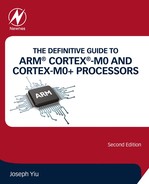
The Sleep-On-Exit feature is ideal for interrupt-driven applications. When it is enabled, the processor can enter sleep as soon as it completes an exception handler and returns to thread mode. It does not cause the processor to enter sleep if the exception handler is returning to another exception handler (nested interrupt). By using Sleep-On-Exit, the microcontroller can stay in sleep mode as much as possible (Figure 19.1).
When the Cortex-M processor enters sleep using Sleep-On-Exit, it is just like executing WFI immediately after the exception exit. However, the unstacking process is not carried out because the registers will have to be pushed on to the stack at the next exception entry. The Sleep-On-Exit feature reduces the power consumption of the system by
1. avoiding unnecessary program execution in thread in interrupt-driven applications and
2. reducing unnecessary stack push and pop operations.
In the case when the processor is woken up by a halt debug request, then the unstacking process will be carried out automatically.
When the Sleep-On-Exit feature is used, the WFE or WFI instruction is normally placed in an idle loop.
SCB->SCR |= SCB_SCR_SLEEPONEXIT_Msk; // Enable Sleep-On-Exit feature
while (1) {
  __DSB(); // Use of memory barrier is recommended for portability
  __WFI(); // Execute WFI and enter sleep
  };
The loop is required because if the processor is woken up by a halt debug request, the instruction after the WFI (branch back to WFI loop) would be executed when the processor is unhalted after debugging.
If you are not using CMSIS-compliant device driver, you can use the following C code to enable the Sleep-On-Exit feature.
#define SCB_SCR (∗((volatile unsigned long ∗)(0xE000ED10)))
/∗ Set SLEEPONEXIT bit in System Control Register ∗/
SCB_SCR = SCB_SCR | 0x2;
Users of assembly language can enable this feature using the following assembly code.
LDR    r0, =0xE000ED10 ; System Control Register address
LDR    r1, [r0]
MOVS   r2, #0x2
ORR    r1, r2 ; Set SLEEPONEXIT bit
STR    r1, [r0]
In interrupt-driven applications, do not enable Sleep-On-Exit feature too early during the initialization. Otherwise if the processor receives an interrupt request during the initialization process, it will enter sleep automatically after the interrupt handler executed, before the rest of the initialization process completes.
19.1.5. Using Send-Event-on-Pend Feature
The Send-Event-on-Pend feature allows any interrupt (including disabled ones) to wake up the processor if the processor entered sleep by executing the WFE instruction. When the SEVONPEND bit in the System Control Register is set, an interrupt switching from inactive state to pending state generates an event, which wakes up the processor from WFE sleep.
If the pending status of an interrupt was already set before entering sleep, a new request from this interrupt during WFE sleep will not wake up the processor.
For users of CMSIS-compliant device driver libraries, the Send-Event-on-Pend feature can be enabled by setting bit 4 in the System Control Register. For example, you can use:
SCB->SCR |= SCB_SCR_SEVONPEND_Msk; /∗ Enable Send-Event-on-Pend ∗/
If you are not using a CMSIS-compliant device driver library, you can use the following C code to carry out the same operation:
#define SCB_SCR (∗((volatile unsigned long ∗)(0xE000ED10)))
/∗ Set SEVONPEND bit in System Control Register ∗/
SCB_SCR |= 1<<4;
Users of assembly language can enable this feature using the following assembly code.
LDR    r0, =0xE000ED10 ; System Control Register address
LDR    r1, [r0]
MOVS   r2, #0x10 ; Set SEVONPEND bit
ORR    r1, r2
STR    r1, [r0]
To utilize the Send-Event-on-Pend feature, the program must execute WFE instruction rather than using WFI or Sleep-On-Exit to enter sleep mode.
19.1.6. Using Wake-up Interrupt Controller
The Wake-up Interrupt Controller (WIC) feature allows the Cortex-M0/Cortex-M0+ processor to enter a sleep state with all clock signals stopped, or even powered down with state retention in the processor logic, while still be able to wake up and resume operations quickly. Details of this feature are covered in Section 9.5.6.
Since the interrupt masking information is transferred between NVIC and WIC automatically using a hardware interface, there is no additional programming step for interrupt management. However, the enabling of some of the ULP states might involve additional device-specific programming steps. For example:
• Depending on the device you are using, you might need to switch on deep sleep mode to use the WIC feature. (Note: in Cortex-M3 r2p0 and r2p1, and Cortex-M4 r0p1, it is necessary to enable deep sleep mode to use the WIC feature. Whereas in Cortex-M0 and Cortex-M0+ processors, both sleep and deep sleep modes can use the WIC feature.)
Apart from these, the presence of the WIC feature is usually transparent to the software.
Since all the clock signals connected to the processor could be stopped in WIC-enabled sleep, the SysTick timer (which is inside the processor) could also be stopped. As a result, it could be necessary to set up a separate peripheral timer to wake up the processor periodically if your application requires an embedded OS and need the OS to operate continuously. In addition, when developing simple applications that need a periodic timer interrupt, and if WIC-mode deep sleep is required, it might be necessary to use a peripheral timer for periodic interrupt generation instead of the SysTick timer even embedded OS is not used.
Not all Cortex-M processor-based microcontrollers support the WIC feature. The reduction of power using the WIC depends on the application and the semiconductor process being used. Currently, the State Retention Power Gating (see Section 9.5.6) technology is only supported in a limited number of silicon technology processes (cell libraries), therefore some chip designs might use the WIC but without using the state retention power down state.
19.1.7. Using Event Communication Interface
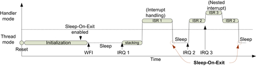
One of the wake-up sources for the WFE sleep operation is an external event signal. (Here the word “external” refers external to the processor boundary. The source generating the event can be on chip or off chip.) The event signal could be generated by on-chip peripherals, or another processor on the same chip. The event communication and WFE can be used together to reduce power in polling loops.
On the Cortex-M processors, there are two signals for event communication:
• TXEV: Transmit Event. A pulse is generated when the SEV instruction is executed.
• RXEV: Receive Event. When a pulse is received on this signal, the event latch inside the processor would be set and can cause the processor to wake up from WFE sleep operation.
First, we look at a simple use of the event connection in a single-processor system: the event can be generated by a number of peripherals. For this example, a DMA controller is illustrated here (Figure 19.2).
In a microcontroller system, a memory block copying process can be accelerated using a DMA controller. If a polling loop is used to determine the DMA status, this will waste energy and consume memory bandwidth and might end up slowing down the DMA operation. To save energy, WFE is used to put the processor into sleep state. When the DMA operation completes, we can then use a “Done” status signal (DMA completed) to wake up the processor and continue program execution.
In the application code, instead of using a simple polling loop that continuously monitor the status of the DMA controller, the polling loop can include WFE instruction as follows:
Enable_DMA_event_mask(); // Write to programmable enable mask register
                         // to enable DMA event
Start_DMA(); // Start DMA operation
do {
    __DSB(); // Use of memory barrier is recommended for portability
    __WFE(); // WFE Sleep operation, wake up when an event is received
} while (check_DMA_completed()==0);
Disable_DMA_event_mask(); // Write to programmable enable mask register
                          // to disable DMA event
Since the processor could be woken up by other events, the polling loop must still check the DMA controller status.
For applications using an embedded OS, an OS-specific delay function should be used instead of using WFE to allow the processor to switch to another task that is waiting to be executed. Using of embedded OS is covered in Chapter 20.
In multiprocessor systems, interprocessor communication such as spin lock often involves polling software flags in shared memory. Similar to the DMA controller example, the WFE sleep operation can be used to reduce power consumption during these activities. In a dual processor system, the event communication interface can be connected in a cross over configuration as shown in Figure 19.3.

In this arrangement, the polling loop for a shared software flag could be written as:
do {
    __DSB(); // Use of memory barrier is recommended for portability
    __WFE(); // WFE Sleep operation, wake up when an event is received
} while (sw_flag_x==0); // poll software flag
task_X(); // execute task X when software flag for task X is received
On the other process that changes “sw_flag_x,” it needs to generate an event after the shared variable is updated. This can be done by executing the SEV (Send event) instruction.
sw_flag_x = 1; // Set software flag in shared memory
__DSB(); // Data synchronization barrier to ensure the write is completed
         // not essential for Cortex-M0/M0+ but is added for software porting
__SEV(); // execute SEV instruction
Using this arrangement, the processor running the polling loop can stay in sleep mode until it receives an event. Since the SEV execution sets the internal event latch, this method works even if the polling process and the process that sets the software variable are running at different times on the same processor, as in a single processor multitasking system.
For applications using an embedded OS, OS-specific event-passing mechanism should be used instead of directly using WFE and SEV.
19.2. Requirements of Low-Power Designs
There are many low-power microcontrollers on the market. Traditionally, many microcontroller vendors classify their microcontrollers as low-power or ULP based on:
• Active current during program execution
• Idle current during sleep
Today, when selecting microcontrollers for low-power applications, designers should also consider:
• Energy efficiency—how much processing work can be done with certain amount of energy.
• Code density—how much program memory is need for an application. ROM (or flash) size requirement can have a significant impact on the system level power.
• Latencies—how long would it take to wake up the processor from sleep, and how long it will take for the processor to complete an interrupt processing task? This can be important for some applications with real-time requirements that the processor might have to run at higher clock frequency to response to an interrupt request quickly.
In many applications, energy efficiency is the key for better battery life. If a microcontroller has lower active current but need several times higher number clock cycles to complete a task, overall it can burn off more power. As a result, the Cortex®-M processors have been very popular in low-power design as they offer excellent energy efficiency as well as high code density.
In addition to longer battery life, there are many other benefits for having energy-efficient processor in low-power designs. For example,
• Smaller battery is required—enable smaller, more portable products
• Low-power requirement might simplify the design of power supply, cooling
• Might enable easier PCB design (thinner power tracks) and thinner wires inside products
• Reduce the electromagnetic interference the microcontroller generates. This can be important to wireless communication product as it affects the quality of the wireless communications
• Enable energy harvesting
19.3. Where Does the Power Go?
To create better low-power design, it would be helpful if we first understand where the power is consumed on a silicon chip. We start by first looking into a photo of a microcontroller die with a Cortex®-M3 processor, as shown in Figure 19.4.
Note on Figure 19.4: Integrated circuit die photo of a STM32F100C4T6B ARM® Cortex-M3 MCU (microcontroller) with 16 KB Flash, 4 KB SRAM, 24 MHz CPU, motor control, and CEC functions.
While it is not clear where the processor is in the photo (it is likely to have merged with the digital logic on the upper right-hand side of the photo, which might also contains digital peripherals, DMA controller, and bus interconnect components), it is clear that the memory blocks (left-hand side) takes a significant space. The bottom right contains some nicely structured components. Some of these blocks could be the analog components (this chip has one 12-bit ADC and two 12-bit DACs).

Figure 19.4 Die of a STM32F100C4T6B ARM Cortex®-M3 microcontroller. Wikipedia (http://en.wikipedia.org/wiki/ARM_Cortex-M).
And next to each of the I/O pads, there are also some transistors to help boosting the drive current and also components for protection and voltage level conversions.
Somewhere in the chip, there are also other clock-related components like three internal oscillators, an external Phase Locked Loop (PLL).
In general, the power consumption of a component in the chip is closely related to its area and its signal toggling activities (Table 19.3).
Table 19.3
Common elements that consume power in a microcontroller
| Components | Description |
| Memories | Typically memories are the most power hungry part of the chip, especially if the microcontroller supports large memory size. The power consumption of the system could also depend on the application code. If the application task is intensive on memory accesses, this can increase the power consumption of the memory system. |
| Processor | Since the Cortex®-M0 and Cortex-M0+ processors are quite small, the actual power consumption of the processor is also fairly small. |
| Peripherals | Some of the peripherals, especially analog peripherals like ADC and DAC can also consume fair amount of power when they are enabled. However, in most all microcontrollers some of these peripherals can often be powered down if they are not used. |
| Oscillators | Some external crystal oscillators could consume fair amount of power when enabled. Many modern microcontrollers have internal RC oscillator which can be lower power but less accurate. |
| I/O pads | When enabled, especially when configured as an output pin, the I/O pad can consume fair amount of power due to the transistor size and potentially, additional power for pull up or pull down support. Many microcontrollers allow the I/O pads to be enabled/disabled via software. |
| Clock distribution network | Hidden in the chip photo there is also a range of transistors that distributes the clock signals to different parts of the chip. These transistors can also consume quite a bit of power when the clock is running. |
Today we see many low-power Cortex-M microcontrollers with very sophisticated system features which enable longer battery life. For example:
• Various run modes and sleep modes available
• Ultralow-power Real Time Clock (RTC), watchdog, and Brown Out Detector (BOD)
• Smart peripherals that can operate while the processor remains in sleep modes
• Flexible clock system control features to allow clock signals for inactive parts of the design to be turned off.
While we will not be able to cover the details of all the low-power features in individual microcontroller devices here, we can cover some of the general concepts. Since different microcontrollers have different low-power features, if you want to fully utilize the low-power capability of the microcontrollers, you need to check out the details of the low-power features from reference materials or examples available from the microcontroller vendors. In many cases, example code could be available for download from the manufacturer Web site.
19.4. Developing Low-Power Applications
19.4.1. Overview of Low-Power Design Practices
In general, there are various measures that can be taken to reduce power consumption:
• Reduction of active power
• Choose the right microcontroller device—Once the basic system and memory size requirements of the project are clear, you can select a microcontroller with enough memory and peripherals but not too much more.
• Run the processor at suitable clock frequency—Many applications do not require a high clock frequency. When a processor is running at high clock speed, it might require wait states due to flash memory access time and hence reduce the energy efficiency.
• Choose the right clock source—Many low-power microcontrollers provide multiple clock sources including internal ones. Depending on the requirements of your applications, some clock sources might work better than others. There is no general rule of “best choice” for which clock source to use. It entirely depends on the application and the microcontroller you are using.
• Do not enable a peripheral unless it is needed—some low-power microcontrollers allow you to turn off clock signals to each peripheral. In some cases, you can even turn off the power supply to certain peripheral to reduce power.
• Other clock system features—Some microcontrollers provide various clock dividers for different parts of the system. You can use these dividers to reduce the power, for example, reduce the processor speed when the processing requirement is low.
• Good power supply design—Good choice of power supply design can provide optimum voltage for the application.
• Reduction of active cycles
• When the processor is idle, sleep modes can be used to reduce power consumption, even it is going to enter sleep only for a short period of time.
• Application code can be optimized for speed to reduce active cycles—In some cases (e.g., C compiler option set to speed optimization), it might increase code size, but when there is spare space in the flash memory then the optimization is worth trying.
• Reduce of power during sleep
• Select the right low-power features—A low-power microcontroller might support various low-power sleep modes. Using the right sleep modes might help you to reduce the power consumption significantly.
• Turn off unneeded peripherals and clock signals during sleep. This can reduce the power consumption, but it might also increase the time required to restore the system to operation state after exiting sleep mode.
• Some microcontrollers can even turn off power supply to some parts inside the microcontroller like flash memory and oscillators during sleeps. But doing this usually needs a longer time to wake up the system.
Most microcontroller vendors would provide code library and example codes to demonstrate the low-power features of their microcontrollers. Those examples can make the application development much easier.
The first step of developing a low-power application is to be familiar with the microcontroller device you are using. A few areas to investigate when developing sleep mode support code included:
• Determine which sleep mode should be used
• Determine which clock signals need to be remain turn on
• Determine if some clock support circuits like crystal oscillators can be switched off
• Determine if clock source switching is needed
19.4.2. Various Approaches to Reduce Power
There are several approaches for creating low-power applications.
Run the Application Quickly and Then Go to Sleep as Much as Possible
This is a very common approach to use. Sleep-mode supports are very common in modern microcontrollers and this approach allows a very good performance margin. So in case there are more interrupt requests arriving than usual, the system can still cope with the processing demand. The down side is that the peak current could be high, and you might need to enable and switch the clock to a fast clock every time the microcontroller wakes up, which could take some time.
Slow Down the Clock as Much as Possible
Many microcontrollers allow you to run the processor at a very slow clock rate, for example, using the RTC 32 KHz oscillator as the processor clock. This enables a much lower active current, and is suitable for applications that only need to deal with periodic tasks where latency to other requests is not an issue.
Power Down and Restart
Depending on the application requirements, some designers choose to power down the microcontroller and configure the microcontroller to wake up on certain hardware events. This can help getting the lowest idle power. But the time required to restart the processor can result in longer response latency, and the restarting process could also consume fair amount of energy.
Some microcontroller vendors include a state retention SRAM and firmware to help shortening the restart process. Firmware APIs could be available to store processor registers and states into the retention SRAM before power down, and the boot loader can then restore the information automatically so that the processor resumes from where it was in the application code. However, there could be some limitations, for example, some processor states like exception status (i.e., IPSR) might not be restored and therefore such power down feature might only be used in thread mode.
Other Possibilities
Some designers have investigated other approaches such as Dynamic Voltage and Frequency Scaling (DVFS) for microcontrollers (mostly academic research studies). However, DVFS is not suitable for some applications because in some microcontrollers, the clock outputs from on-chip PLL is unstable during switching and the PLL switching time could be too long to allow such system to deal with interrupt requests in real time. In addition, this method is unsuitable for many microcontrollers where the peripherals are operating on a clock derived from the processor's clock and require a constant clock speed.
19.4.3. Selecting the Right Approach
The actual selection of the low-power approach depends on many device-specific factors and application-specific requirements. For example, if in your application it might have to deal with unpredictable processing loading requirements, then it is better to run the processor faster so that it can cope with occasional high processing demand periods, and get the system to sleep mode as long as possible. However, running the clock faster than needed can also have drawbacks:
• Excessive power consumption on the oscillator, and potentially high power wastage in the PLL (if used).
• Clock signals going to some of the peripherals could still be on all the time. If available, consider utilizing some of the clock prescalars to reduce the clock speed of certain peripherals.
You can also consider running the clock in a medium frequency range, and only increase the clock speed when certain processing tasks (that require longer execution time) are executed.
In some applications, you could find that instead of using a PLL to get a high clock frequency, you can use a higher frequency crystal and use clock prescalar to reduce the processor's clock to lower operating frequency when the work load is low. If the processing requirement increases, then reprogram the prescalar to increase the processor's clock speed. This avoids the need to use the PLL (especially if the PLL is power hungry) and reduce the clock speed switching time (reprogram a clock prescalar is normally much faster than a PLL frequency switch).
In applications that the role of the processor is just to wake up periodically and do some processing, and the processing latency is not an issue, then running the clock slow could be one good way to reduce power. This is particularly useful for systems based on energy harvesting because it reduces the peak current to a minimum. However, there are some cases where running the clock as slow as possible might not able to save energy:
• At low frequency range, the power consumption does not necessarily reduce linearly as the clock rate reduced due to leakage current, or active power of external components connected to the microcontroller. If the leakage current of the system is high, then running the system for longer can increase the power consumed due to leakage current. This is particularly true for microcontroller devices with memories that have high leakage current, or when certain analog components need to be turned on throughout the processing. If the leakage current is much lower during sleep, running the system faster and putting it into sleep mode longer might save more power.
• There can be various limitations of frequency range and low-power characteristics of the oscillator and clock circuit designs. If the oscillator and PLL power consumption is significant and the power of these components cannot be able to reduce any further under certain frequency range, then reducing clock frequency further lower is not going to help.
• Do not use a crystal with frequency lower than the specified frequency range stated by the microcontroller data sheet. Not only the crystal oscillator might not be able to startup properly, it might end up with harmonic in the oscillation which might result in an unreliable system and the oscillator could consume more power. It is also important to use the right capacitors with the crystal as stated in data sheet.
For applications that stay in sleep mode for extensive amount of time and if wake-up latency is not an issue, power down the design when the system is idle could be the best choice. In such case, care must be taken to reduce the power consumed in the start-up sequence. For example, a slow oscillator (e.g., 32 KHz) might take much longer time than a fast crystal oscillator to startup, therefore could end up with higher start-up energy consumption.
19.5. Debug Considerations
19.5.1. Debug and Low-Power
Depending on the microcontroller devices used, in some cases the sleep modes can disable all the clock signals or can disable the signal paths for debug connections. In such cases, if you are running a debug session on a debug host and such sleep mode is used, the debug session would terminate as the debugger can no longer talk to the chip.
In some other cases, you might find that when a debugger is connected, it disables certain low-power features so that the debug session can continue during sleep. However, the power of the system during debug will not reflect the real-world scenarios (it will be higher).
19.5.2. “Safe Mode” for Debug and Flash Programming
If you are using a microcontroller device that could terminate your debug connection during sleep mode, and if you are developing an application that could go into sleep mode fairly quickly after the system powers up, you could find that your microcontroller device get locked out from the debug connections after the program image is programmed. This is because the debugger does not have enough time to connect to the device before the sleep mode takes place (unless you can force the processor clock to run very slowly). This could also prevent you from updating the program image in the flash, because that also requires a debug connection.
For this case, you should consider adding a “safe mode” at the starting of the application so that the device will not go into sleep mode, or at least, not immediately when the safe mode is activated. Alternatively, the safe mode can force the application to use a sleep mode that does not disconnect the debugger. Such safe mode can be implemented by adding a simple status check on an input pin at start-up.
In some microcontroller devices, there are boot mode configurations and you can use that to enable flash programming instead of using a safe mode. However, the “safe mode” feature in the application is still useful for enabling debug operations.
19.5.3. Debug Interface and Low-Voltage Pins
Some microcontrollers can work at low voltage supply and this enables them to have very low-power consumption. However, some debug adaptors are not designed for low-voltage debug interface. As a result, you might need to increase the supply voltage for the development board during software development, or to get a debug adaptor that can operate at lower voltage.
19.6. Benchmarking of Low-Power Devices
19.6.1. Background of ULPBench™
Currently, most microcontroller vendors describe the low-power characteristic of their products by quoting active current and idle current. However, as highlighted in the beginning of Section 19.2, this is no longer enough for designers. As there were no standardized rules of how active current should be measured, some of the quoted active current from microcontroller vendors could be controversial because:
• The data can be obtained by running “while(1)”—the instruction could be fetched from a prefetch buffer and therefore no memory access activity in the flash and SRAM.
• The data can be obtained by running program code from SRAM, with the flash memory turned off.
• The data can be obtained by running program with wait states for flash memory enabled. This reduces the signal toggling and therefore reduces power.
• The test could be carried out with a voltage supply that is only suitable for labs environment and is not suitable for real-world applications.
As a result, there is a need to come up a standardize way to demonstrate energy efficiency in low-power microcontroller devices.
Although it is possible to use existing benchmark code like EEMBC® CoreMark® as a reference for measuring power, the data processing complexity of CoreMark is somewhat overkill for a lot of the ULP applications. On the other hand, Dhrystone is too small to illustrate processing requirements and therefore is not suitable either.
There is also the need to demonstrate the sleep mode current. If the program execution is too long, the active power will dominate the test result.
As a result, the EEMBC ULPBench workgroup was formed in 2012. The aim of the work group is to create benchmark suites that are suitable for measuring energy efficiency of low-power and ULP microcontroller devices, with a consistent and well-defined method.
The ULPBench project is divided into multiple phases. The first phase focuses on the energy efficiency of the processors inside the microcontroller, and is named ULPBench-Core Profile (or ULPBench-CP). Currently, additional profiles are being discussed and investigated in the EEMBC ULPBench workgroup.
19.6.2. Overview of the ULPBench-CP
The score of the ULBench-CP is to measure the energy efficiency of ULP microcontroller devices, including 8-, 16-, and 32-bit devices. Unlike traditional benchmarks, the ULPBench needs a piece of hardware to measure the actual energy consumption by a device. Therefore the ULPBench-CP has defined:
• A workload (in C language) that can be used on 8-, 16-, and 32-bit architectures,
• A reference energy measurement hardware, called the EnergyMonitor,
• A Windows-based GUI to access the measurement hardware and control the test process and to display and compute the results.
In order to reflect the work load pattern of real-world applications, the workload executes a workload once every second and enter sleep mode the rest of the time (Figure 19.5).
The measurement process spans 10 occurrences of the processing. In order to ensure the data is accurate, 12 occurrences of the processing are needed and the software controlling the test detects the middle 10 occurrences and uses them for calculation of benchmark result.
The workload contains data processing functions including:
• Data processing of 8-, 16-, and 32-bit data types,
• Control functions (7-segment LCD),
• Sorting,
• String functions,
• Task scheduling.

A simple task scheduler is included as part of the workload, but no actual context switching takes place because such operation is not supported by a number of 8-bit microcontrollers targeting ULP applications.
On existing Cortex®-M0, Cortex-M0+, Cortex-M3, and Cortex-M4 processors, the execution time of the workload takes around 10–14 k clock cycles. So if you wish, you can execute the workload with an on-chip 32-KHz crystal provided it has the required accuracy (±50 ppm).
To support the measurement setup, EEMBC provides a reference hardware tool called EnergyMonitor that you can buy from EEMBC Web site, and a software running on a personal computer to collect the data from EnergyMonitor and compute the result. The EnergyMonitor hardware is shown in Figure 19.6.
The Energy Monitor receives the power from the USB connector, and supplies the power to the DUT (Device Under Test) using jumper connector (Figure 19.7).
Some software porting work is required to get the ULPBench-CP working on a microcontroller. ARM® has already contributed a template for the Cortex-M processors, but software developers need to add device-specific low-power feature support code, and might need to port the timer code to use device-specific low-power timer instead of the generic SysTick timer for best results. Also, some I/O control functions are defined in ULPbench-CP to indicate that the system is indeed running ULPBench-CP correctly (signal toggling can be observed with an oscilloscope). These functions also need to be ported.
After the software porting work is done, we can then test the ULPBench-CP with the ULPBench EnergyMonitor software. The measurement process is repeated a number of times before the score were computed. The result can then be optionally uploaded to the EEMBC Web site for display. Figure 19.8 shows the ULPBench-CP test result of a STM32L476, a microcontroller with Cortex-M4 with FPU processor, 1 MB on-chip flash and 12 KB of SRAM, which has an impressive official score of 123.5 ULPMark™-CP. Additional ULPBench-CP scores can be found on EEMBC Web site.1


Unlike traditional power measurement tools, the EnergyMonitor essentially measures the charging time of a capacitor which supplies current to the device under test. Unlike ADC sampling, this method provides higher accuracy by avoiding any error stemming from current spikes between samples.
In order to make sure the test provides a fair and equitable comparison, the measurement setup has a number of requirements:
• The supply voltage is 3 V.
• The wake-up timer must be accurate (within ±50 ppm).
• The program code must run from the microcontroller's flash memory (or NVM).
The benchmark result is represented as ULPMark-CP = 1000/(median of 5 times average energy per second for 10 ULPBench cycles). The energy is measure in microjoules.

19.7. Example of Using Low-Power Features on Freescale KL25Z
19.7.1. Objective
The aim of this test example is to generate a 1-Hz- period interrupt to output a message via the UART interface, and have the processor put in low-power mode to reduce the overall current as much as possible.
In this example, we assume that the timing of the wake-up event needs to be very accurate. As a result, we use the external crystal for the clock source during operation.
19.7.2. Test Setup
The test is based on the Freescale Freedom board (FRDM-KL25Z). In this development board, you can do a small modification so that you can measure the electric supply current going into the microcontroller by connecting an ammeter across jumper J4 (Figure 19.9).
• If you are using REV-D of the FRDM-KL25Z, there is a solder shorter right under jumper J4 that you need to cut out.
• If you are using REV-E of the FRDM-KL25Z, there are two resistors connected across J4 and both are placed next to J4: a 0 Ω (R73) and a 10 Ω (R81). If you want to measure the current using an ammeter, you should desolder both of them. Alternatively you can remove just the 0-Ω resister and measure the current using a voltmeter.

After doing the modification, you can put the board back into normal operations again by putting a jumper header on jumper J4. In case you want to find out more about the differences between the REV D and REV E of the Freedom board, Erich Styger wrote a very good blog about this which can be found in http://mcuoneclipse.com/2013/06/09/frdm-kl25z-reve-board-arrived/.
19.7.3. Low-Power Modes on KL25Z
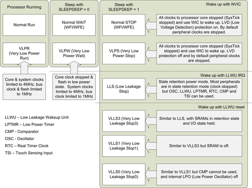
The KL25Z128VL microcontroller device supports a number of power modes, as shown in Figure 19.10.
In this example, we use the VLPS (Very Low Power Stop) mode. Alternatively LLS (Low Leakage Stop) could be used but the UART will be stopped during sleep. If the processor entered sleep before the UART transmission completed, the output UART data could be corrupted.
The selection of the operation mode is handled by a unit called System Mode Controller (SMC).
19.7.4. Clocking Arrangement
The clock generation involved several components, as illustrated in Figure 19.11. This included:
• Multipurpose Clock Generator (MCG)—This unit contains the internal RC oscillators (4 MHz and 32 KHz), a Frequency Locked Loop (FLL) and a Phase Locked Loop (PLL). The FLL and PLL can utilize the clock generated from the System Oscillator.
• System Integration Module (SIM)—This unit provides various clock multiplexing/routing/prescaling options, as well as controls the clocks to peripherals.
• Power Management Controller (PMC)—This unit contains the internal voltage regulator, power on reset (POR), and low-voltage detect system. (Not used in this example.)
• Real Time Clock (RTC)—Generate Timer interrupts and a 1-Hz clock. (Not used in this example.)
Instead of using RTC for the 1-Hz interrupt generation, we use the LPTMR (Low-Power Timer) because the external crystal is connected to an 8-MHz crystal. The RTC works best with an external 32-KHz crystal.

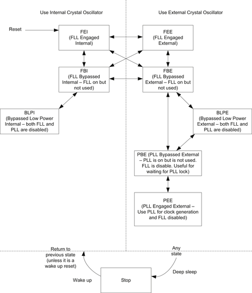
To make things slightly more challenging, software developers also need to understand the operation states of the MCG (Figure 19.12).
In our example, the system starts-up in FEI state, then switches the FBE state, and then switches to BLPE state. The switching of the operation states are done inside the “SystemInit()” function at start-up.
19.7.5. The Test Setup
The overview of the setup can be summarized as:
• For first step of our experiment, the microcontroller uses Normal Run and Normal Stop. The system runs on 8-MHz clock frequency.
• Then we enhance the design to use Very Low-Power Run (VLPR) and Very Low-Power Stop (VLPS) modes to further reduce the power.
• The wake-up source selected is the Low-Power Timer (LPTMR) module.
The setup of the MCG is easy. The control code is already included in the default.
"system_MKL25Z4.c". We only need to select the define option in this file:
#define DISABLE_WDOG    1

#define CLOCK_SETUP    2
/∗ Predefined clock setups
   0 … Multipurpose Clock Generator (MCG) in FLL Engaged Internal (FEI) mode
       Reference clock source for MCG module is the slow internal clock source
       32.768kHz
       Core clock = 41.94MHz, BusClock = 13.98MHz
   1 … Multipurpose Clock Generator (MCG) in PLL Engaged External (PEE) mode
       Reference clock source for MCG module is an external crystal 8MHz Core clock = 48MHz, BusClock = 24MHz
   2 … Multipurpose Clock Generator (MCG) in Bypassed Low Power External (BLPE)
       mode
       Core clock/Bus clock derived directly from an external crystal 8MHz with
       no multiplication
       Core clock = 8MHz, BusClock = 8MHz
∗/
The code to get the system running is as follows. Please note that at the start of the test program, a UART input function is called so that the test does not start until it has received a character from the UART interface. This prevents the board from being locked out completely by the low-power mode and allow the program flash to be reprogrammed (see safe mode operation in 19.5.2).
Once this is working, the "void Low_Power_Config(void)" function is updated to include the additional enhancement:
• To enable the use of VLPR and VLPS modes, we need to reduce the clock frequency of the system from 8 MHz to a lower frequency at 4 MHz or lower. A frequency value of 1 MHz is selected.
• To save more power, the flash memory is turned off during sleep (this is referred as Flash Doze feature in Freescale document).
• Turn off internal oscillator.
• Enable the very-low power modes by programming to the System Mode Controller (SMC) module.
The modified “void Low_Power_Config(void)” function is as follows.
19.7.6. Measurement Results
After the test is created, several measurements were made (Table 19.4). Please note that the measurements should be made without debugger connected. Note: Due to the limitation of the multimeter used and other potential factors in the setup (e.g., potentially activities of the onboard SDA debugger chip might have affected the debug operation state), the results shown here might not be accurate.
The sleep current of 1.27 mA seems a bit high. With a CR2032 coin cell of 225 mAh, this gives only 177 h of operations (just over 1 week). However, the KL25Z data sheet quotes the power of using an external 4 MHz crystal adds around 228 μA electric current. Since we are using an 8-MHz crystal, the actual power used by the external crystal oscillator can be quite significant. In addition, the 8-MHz clock routing paths to peripherals (e.g., clock buffers and capacitance of clock lines) can also contribute to the higher power.
Table 19.4
Test results with 8-MHz clock source
| Condition | Current |
| Running the processor at 8 MHz without entering sleep | 3.23 mA |
| Running the processor at 1 MHz without entering sleep (Note: Oscillator still running at 8 MHz) | 2.52 mA |
| Sleep current | 1.27 mA |
In order to double check how the system power can be further reduced, the test setup is modified to use the internal 4-MHz RC oscillator. The “SystemInit()” function is edited to add a new clock setup so that the system is Started with MCG unit in BLPI (Bypassed Low Power Internal) mode. The processor and bus clocks are reduced to 1 MHz by the clock dividers (Table 19.5).
To help investigate the power activities, a 10-Ω resistor can be used to connect along the voltage supply connection and the voltage across the resistor can be measured with an oscilloscope (Figure 19.13). However, due to the small electrical current in this test, the result cannot be read from the graph accurately.
Assume that most of the time the microcontroller is sleeping (using 0.04 mA), this now gives us 5500 h, or over 200 days of battery life from a single CR2032 battery.
Additional power saving could be possible by reducing the active cycles. For example, by using interrupt-driven mechanism to output the text string into the UART, instead of polling-based UART function, could help. However, an experimental trial of changing the printf message to just output one character do not seems to be able to reduce the power consumption. This potentially highlight that the majority of the power is not consumed by the processor or the UART, but could be by other components inside the chip.

The active cycles can also be reduced by compiler optimizations and software optimizations. Also, potential delay could also be resulted if some of the bus clock frequency and memory clock speed are set too low. It is important to carefully investigate the clock frequency requirements for each part of the design.
If the application is not using the UART interface, potentially we can run the system at a much lower clock frequency. According to the datasheet, the electric current of the oscillator can be reduced to ∼0.5 μA if using a 32 KHz. Also, with such arrangement, the RTC can be used for the periodic 1-Hz interrupt generation instead of the Low-Power Timer module.
Do not forget that we have not utilized all the low-power modes in the KL25Z design yet. There are a number of other low-leakage power modes available and can further reduce the idle/sleep current.
..................Content has been hidden....................
You can't read the all page of ebook, please click here login for view all page.