Appendix E
Debug Registers Quick Reference
E.1. Overview
The debug systems in the Cortex®-M0 and Cortex-M0+ processors contain a number of programmable registers. These registers can be accessed by in-circuit debuggers only and cannot be accessed by the application software. This quick reference is intended for tools developers, or if you are using a debugger that supports debug scripts (e.g., ARM® DS-5), where you can use debug scripts to access these registers to carry out testing operations automatically.
The debug system in the Cortex-M0 and the Cortex-M0+ processors is partitioned into as follows:
• Debug support in the processor core,
• Breakpoint unit,
• Data watchpoint unit,
• ROM table,
• and optionally, a Micro Trace Buffer (MTB) for Cortex-M0+ processor.
System-on-Chip developers can add additional debug support components if required. If additional debug components are added, an additional ROM table unit could also be added to the system so that a debugger can identify available debug components included in the system.
The debug support is configurable; for example, some Cortex-M0/M0+ devices might not have any debug support, and some Cortex-M0+ devices might not have MTB support.
E.2. Core Debug Registers
The processor core contains a number of registers for debug purpose (Table E.1).
Table E.1
Summary of core debug registers
| Address | Name | Descriptions |
| 0xE000ED24 | SHCSR | System Handler Control and State Register—indicate system exception status. |
| 0xE000ED30 | DFSR | Debug Fault Status Register—Allow debugger to determine the cause of halting. |
| Table Continued | ||

| Address | Name | Descriptions |
| 0xE000EDF0 | DHCSR | Debug Halting Control and Status Register—Control processor debug activities like halting, single stepping |
| 0xE000EDF4 | DCRSR | Debug Core Register Selector Register—control read and write of core registers during halt |
| 0xE000EDF8 | DCRDR | Debug Core Register Data Register—data transfer register for reading or writing core registers during halt |
| 0xE000EDFC | DEMCR | Debug Exception Monitor Control Register—for enabling of data watchpoint unit and vector catch feature. Vector catch allows the debugger to halt the processor if the processor is reset, or if a HardFault exception is triggered. |
| 0xE000EFD0 to 0xE000EFFC | PIDs, CIDs | ID registers |

System Handler Control and State Register (0xE000ED24)
| Bits | Field | Type | Reset value | Descriptions |
| 31:16 | Reserved | – | – | Reserved |
| 15 | SVCALLPENDED | RO | 0 | 1 indicates SVC execution is pended. Accessible from debugger only. |
| 14:0 | Reserved | – | – | Reserved |

Debug Fault Status Register (0xE000ED30)
| Bits | Field | Type | Reset value | Descriptions |
| 31:5 | Reserved | – | – | Reserved |
| 4 | EXTERNAL | RWc | 0 | EDBGRQ was asserted |
| 3 | VCATCH | RWc | 0 | Vector catch occurred |
| 2 | DWTTRAP | RWc | 0 | Data watchpoint occurred |
| 1 | BKPT | RWc | 0 | Breakpoint occurred |
| 0 | HALTED | RWc | 0 | Halted by debugger or single stepping |

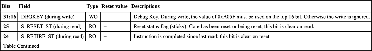
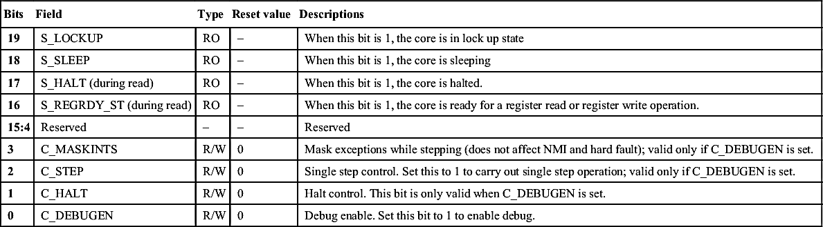
Debug Halting Control and Status Register (0xE000EDF0)
| Bits | Field | Type | Reset value | Descriptions |
| 31:16 | DBGKEY (during write) | WO | – | Debug Key. During write, the value of 0xA05F must be used on the top 16 bit. Otherwise the write is ignored. |
| 25 | S_RESET_ST (during read) | RO | – | Reset status flag (sticky). Core has been reset or being reset; this bit is clear on read. |
| 24 | S_RETIRE_ST (during read) | RO | – | Instruction is completed since last read; this bit is clear on reset. |
| Table Continued | ||||
| Bits | Field | Type | Reset value | Descriptions |
| 19 | S_LOCKUP | RO | – | When this bit is 1, the core is in lock up state |
| 18 | S_SLEEP | RO | – | When this bit is 1, the core is sleeping |
| 17 | S_HALT (during read) | RO | – | When this bit is 1, the core is halted. |
| 16 | S_REGRDY_ST (during read) | RO | – | When this bit is 1, the core is ready for a register read or register write operation. |
| 15:4 | Reserved | – | – | Reserved |
| 3 | C_MASKINTS | R/W | 0 | Mask exceptions while stepping (does not affect NMI and hard fault); valid only if C_DEBUGEN is set. |
| 2 | C_STEP | R/W | 0 | Single step control. Set this to 1 to carry out single step operation; valid only if C_DEBUGEN is set. |
| 1 | C_HALT | R/W | 0 | Halt control. This bit is only valid when C_DEBUGEN is set. |
| 0 | C_DEBUGEN | R/W | 0 | Debug enable. Set this bit to 1 to enable debug. |
Debug Core Register Selector Register (0xE000EDF4)
| Bits | Field | Type | Reset value | Descriptions |
| 31:17 | Reserved | – | – | Reserved |
| 16 | REGWnR | WO | – | Set to 1 to write value to register Set to 0 to read value from register |
| 15:5 | Reserved | – | – | Reserved |
| 4:0 | REGSEL | WO | 0 | Register select |

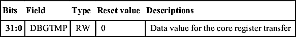
Debug Core Register Data Register (0xE000EDF8)
Debug Exception and Monitor Control Register (0xE000EDFC)
| Bits | Field | Type | Reset value | Descriptions |
| 31:25 | Reserved | – | – | Reserved |
| 24 | DWTENA | RW | 0 | Data Watchpoint unit enable. |
| 23:11 | Reserved | – | – | Reserved |
| 10 | VC_HARDERR | RW | 0 | Debug trap at hard fault exception |
| 9:1 | Reserved | – | – | Reserved |
| 0 | VC_CORERESET | RW | 0 | Halt processor after system reset and before the first instruction executed. |

E.3. Breakpoint Unit
The breakpoint unit contains up to four comparators for instruction breakpoints. Each comparator can produce a breakpoint for up to two instructions (if the two instructions are located in the same word address). Additional breakpoints can be implemented by inserting breakpoint instructions in the program image if the program memory can be modified (Table E.2).
The breakpoint unit design is configurable. Some microcontrollers might contain no breakpoint unit, or a breakpoint unit with less than four comparators.
Table E.2
Summary of registers in the breakpoint unit
| Address | Name | Descriptions |
| 0xE0002000 | BP_CTRL | Breakpoint Control Register—for enabling the breakpoint unit and provide information about the breakpoint unit. |
| 0xE0002008 | BP_COMP0 | Breakpoint Comparator Register 0 |
| 0xE000200C | BP_COMP1 | Breakpoint Comparator Register 1 |
| 0xE0002010 | BP_COMP2 | Breakpoint Comparator Register 2 |
| 0xE0002014 | BP_COMP3 | Breakpoint Comparator Register 3 |
| 0xE0002FD0 to 0xE0002FFC | PIDs, CIDs | ID registers |
Breakpoint Control Register (0xE0002000)
| Bits | Field | Type | Reset value | Descriptions |
| 31:17 | Reserved | – | – | Reserved |
| 7:4 | NUM_CODE | RO | 0 to 4 | Number of comparators |
| 3:2 | Reserved | – | – | Reserved |
| 1 | KEY | WO | – | Write Key. When write to this register, this bit should be set to 1, otherwise the write operation is ignored. |
| 0 | ENABLE | RW | 0 | Enable control |

Breakpoint Comparator Registers (0xE0002008–0xE0002014)
| Bits | Field | Type | Reset value | Descriptions |
| 31:30 | BP_MATCH | RW | – | Breakpoint setting: 00: No breakpoint 01: Breakpoint at lower half word address 10: Breakpoint at upper half word address 11: Breakpoint at both lower and upper half word |
| 29 | Reserved | – | – | Reserved |
| 28:2 | COMP | RW | – | Compare instruction address |
| 1 | Reserved | – | – | Reserved |
| 0 | ENABLE | RW | 0 | Enable control for this comparator |

E.4. Data Watchpoint Unit
The data watchpoint unit (DWT) has two main functions:
• Setting data watchpoints
• Providing a Program Counter (PC) sampling register for basic profiling.
Before accessing the DWT, the DWTENA bit in Debug Exception and Monitor Control Register (DEMCR, address 0xE000EDFC) must be set to 1 to enable the DWT. Unlike the Data Watchpoint and Trace unit in Cortex®-M3/M4, the DWT in the Cortex-M0 and Cortex-M0+ processors does not support trace. But the programming models of its registers are mostly compatible to the DWT in ARM®v7-M (Table E.3).
The DWT design is configurable. Some microcontrollers might contain no DWT, or a DWT with just one comparator.
Table E.3
| Address | Name | Descriptions |
| 0xE0001000 | DWT_CTRL | DWT Control Register—provide information about the data watchpoint unit. |
| 0xE000101C | DWT_PCSR | Program Counter Sample Register—provide current program address |
| 0xE0001020 | DWT_COMP0 | Comparator Register 0 |
| 0xE0001024 | DWT_MASK0 | Mask Register 0 |
| 0xE0001028 | DWT_FUNCTION0 | Function Register 0 |
| 0xE0001030 | DWT_COMP1 | Comparator Register 1 |
| 0xE0001034 | DWT_MASK1 | Mask Register 1 |
| 0xE0001038 | DWT_FUNCTION1 | Function Register 1 |
| 0xE0001FD0 to 0xE0001FFC | PIDs, CIDs | ID registers |
DWT Control Register (0xE0001000)
| Bits | Field | Type | Reset value | Descriptions |
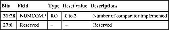
| 31:28 | NUMCOMP | RO | 0 to 2 | Number of comparator implemented |
| 27:0 | Reserved | – | – | Reserved |
Program Counter Sample Register (0xE000101C)
| Bits | Field | Type | Reset value | Descriptions |
| 31:0 | EIASAMPLE | RO | – | Execution instruction address sample. Read as 0xFFFFFFFF is core is halted or if DWTENA is 0. |

DWT COMP0 Register and DWT COMP1 Registers (0xE0001020, 0xE0001030)
| Bits | Field | Type | Reset value | Descriptions |
| 31:0 | COMP | RW | – | Address value to compare to. The value must be aligned to the compare address range defined by the compare mask register. |

DWT MASK0 Register and DWT MASK1 Registers (0xE0001024, 0xE0001034)
| Bits | Field | Type | Reset value | Descriptions |
| 31:4 | Reserved | – | – | Reserved |
| 3:0 | MASK | RW | – | Mask pattern: 0000: compare mask = 0xFFFFFFFF 0001: compare mask = 0xFFFFFFFE … 1110: compare mask = 0xFFFFC000 1111: compare mask = 0xFFFF8000 |

DWT FUNC0 Register and DWT FUNC1 Registers (0xE0001028, 0xE0001038)
| Bits | Field | Type | Reset value | Descriptions |
| 31:4 | Reserved | – | – | Reserved |
| 3:0 | FUNC | RW | 0 | Function: 0000: Disabled 0100: Watchpoint on PC match 0101: Watchpoint on read address 0110: Watchpoint on write address 0111: Watchpoint on read or write address Other values: Reserved |

E.5. ROM Table Registers
The ROM table is used to allow a debugger to identify available components in the system. The lowest two bits of each entry are used to indicate if the debug component is present, and if there is another valid entry following in the next address in the ROM table. The rest of the bits in the ROM table contain the address offset of the debug unit from the ROM table base address.
| Address | Value | Name | Descriptions |
| 0xE00FF000 | 0xFFF0F003 | SCS | Points to System Control Space base address 0xE000E000 |
| 0xE00FF004 | 0xFFF02003 | DWT | Points to DW base address 0xE0001000 |
| 0xE00FF008 | 0xFFF03003 | BPU | Points to BPU base address 0xE0002000 |
| 0xE00FF00C | 0x00000000 | end | End of table marker |
| 0xE00FFFCC | 0x00000001 | MEMTYPE | Indicates that system memory is accessible on this memory map. |
| 0xE00FFFD0 to 0xE00FFFFC | 0x000000–– | IDs | Peripheral ID and component ID values (values dependent on the design versions). |

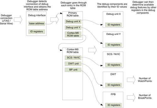
Using the ROM table, the debugger can identify the debug components available as shown in Figure E.1.
The ROM table look-up can be divided into multiple stages if a System-on-Chip design contains additional debug components and an extra ROM table. In such cases the ROM table look-up can be cascaded, as shown in Figure E.2, so that the debugger can identify all the debug components available.

E.6. Micro Trace Buffer
E.6.1. Overview
The MTB component provides instruction trace feature for the Cortex®-M0+ processor (Table E.4). It is an optional component and the base address of the MTB is device dependent. The full details of the MTB are covered in the CoreSight™ MTB-M0+ Technical Reference Manual (TRM, reference 15), which can be downloaded from ARM® Web site.
Table E.4
| Address | Name | Descriptions |
| Base address + 0x0 | POSITION | Position of the trace pointer |
| Base address + 0x4 | MASTER | Various control information, including memory size allocated for trace buffer. |
| Base address + 0x8 | FLOW | Control watermark level, and what actions to take when the trace pointer reached water mark level. |
| Base address + 0xC | BASE | The base address of the SRAM |
| Base address + 0xF00 to 0xFFC | CoreSight registers | Registers for CoreSight device management and identifications |
E.6.2. POSITION Register
| Bits | Field | Type | Reset value | Descriptions |
| 31:N | – | – | 0 | Unimplemented bits of POINTER. Read as zero, write ignored. |
| N:3 | POINTER | RW | – | Relative address for the next trace packet (the address must be multiple of 8 because each packet contains two words). Width of POINTER depends on the SRAM size connected to the MTB. Physical address of pointer is POINTER + BASE. |
| 2 | WRAP | RW | – | This bit is set to 1 automatically when the POINTER value wraps when reaching to the end of the allocated space. |
| 1:0 | Reserved | – | – |

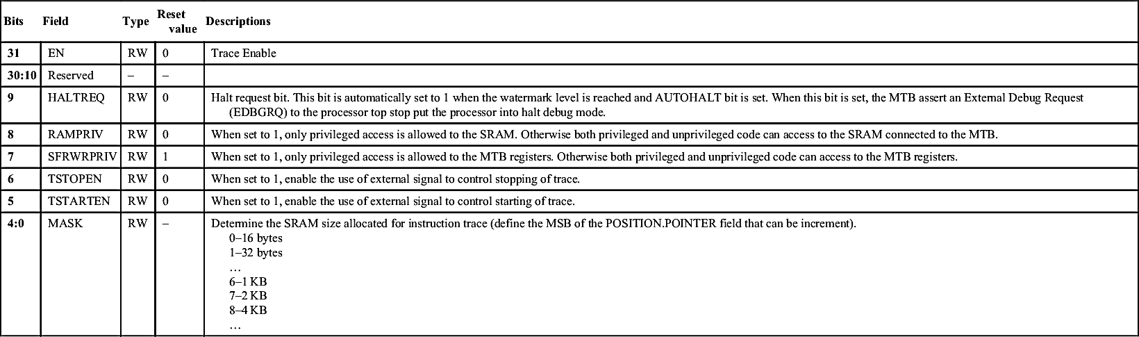
E.6.3. MASTER Register
| Bits | Field | Type | Reset value | Descriptions |
| 31 | EN | RW | 0 | Trace Enable |
| 30:10 | Reserved | – | – | |
| 9 | HALTREQ | RW | 0 | Halt request bit. This bit is automatically set to 1 when the watermark level is reached and AUTOHALT bit is set. When this bit is set, the MTB assert an External Debug Request (EDBGRQ) to the processor top stop put the processor into halt debug mode. |
| 8 | RAMPRIV | RW | 0 | When set to 1, only privileged access is allowed to the SRAM. Otherwise both privileged and unprivileged code can access to the SRAM connected to the MTB. |
| 7 | SFRWRPRIV | RW | 1 | When set to 1, only privileged access is allowed to the MTB registers. Otherwise both privileged and unprivileged code can access to the MTB registers. |
| 6 | TSTOPEN | RW | 0 | When set to 1, enable the use of external signal to control stopping of trace. |
| 5 | TSTARTEN | RW | 0 | When set to 1, enable the use of external signal to control starting of trace. |
| 4:0 | MASK | RW | – | Determine the SRAM size allocated for instruction trace (define the MSB of the POSITION.POINTER field that can be increment). 0–16 bytes 1–32 bytes … 6–1 KB 7–2 KB 8–4 KB … |
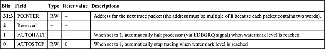
E.6.4. FLOW Register
| Bits | Field | Type | Reset value | Descriptions |
| 31:3 | POINTER | RW | – | Address for the next trace packet (the address must be multiple of 8 because each packet contains two words). |
| 2 | Reserved | – | – | |
| 1 | AUTOHALT | – | – | When set to 1, automatically halt processor (via EDBGRQ signal) when watermark level is reached. |
| 0 | AUTOSTOP | RW | 0 | When set to 1, automatically stop tracing when watermark level is reached |
E.6.5. BASE Register

E.6.6. Packet Format
Each of the MTB packets is two words in size (Figure E.3). The packet address must be aligned to multiple of 8 bytes.

Since an instruction address must be aligned to half-word aligned address, the bit 0 of each word in an MTB packet can be used for other information, the S bit and A bit (Table E.5):
Table E.5
Definition of the S bit and A bit in an MTB packet
| Bit | Descriptions |
| S bit | Start bit. If this bit is 1, it indicates that the trace was previously has been stopped and this packet is the start of a new sequence. During a trace session, the trace could be stopped and started again using external controlled signal (when MASTER.TSTARTED and MASTER.TSTOPED bits are set) |
| A bit | Atomic bit. Indicates the type of branch. If this bit is 0, it indicates a normal branch operation. The source address field indicates the address of the instruction that trigger the branch. If this bit is 1, it indicates exception entry or a PC update in a debug state. The source address field indicates the return address for the exception, or the address of the instruction that was to be executed before entering debug state. |
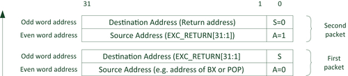
In exception returns, two MTB packets are generated (Figure E.4).
E.6.7. Examples
Take an example that a microcontroller has an SRAM connected to the MTB which is 32 KB in size, and the address of the SRAM is at 0x20000000 (Figure E.5). The BASE register should read as 0x20000000.

Since the size of the SRAM is 32 KB, only bit[14:2] of the POSITION register is implemented. A debugger can detect the maximum size of the SRAM by writing 0xFFFFFFF8 to the POSITION register, and get 0x00007FF8 back.
For instruction trace, we would like to allocate only the last 4 KB of the SRAM. The first 28 KB of the SRAM is still used by the application code.
To enable such arrangement, we can program the MTB as:
• POSITION = 0x00007000 (Trace buffer starting address = BASE + 0x00007000)
• FLOW = 0 (watermark)
• MASTER = 0x80000008 (FIELD = 0x8, the highest bit that can be toggled by pointer increment is bit 8 (512 × 8 bytes = 4 KB). EN bit set to 1 to enable trace)
To disable trace, we can just clear the EN bit in MASTER:
• MASTER = 0x00000008
After the trace is done, the debugger can read the POSITION register to deter the ending location of the trace, read the trace buffer backward and identify the start of the trace by checking the S-bit. If the TSTARTEN and TSTOPEN bits are used in the trace setup, there can be multiple trace sessions and the debugger should read through the whole 4 KB allocated buffer to see if there are multiple sessions of instruction trace.
..................Content has been hidden....................
You can't read the all page of ebook, please click here login for view all page.