
Memory Systems
Publisher Summary
Since the Cortex™-M3 processor has different memory architecture from that of traditional ARM processors, the different features of its memory systems are explained in this chapter. The memory map shows what is included in each memory region. Aside from decoding which memory block or device is accessed, the memory map also defines the memory attributes of the access. The different memory attributes and its regions are described here. Access permissions for default memory are also discussed. Bit-band operations allow a single/store operation to access a single data bit. The chapter also provides details about unaligned transfers and what it looks like. The Cortex-M3 has no SWP instruction (swap), which is now replaced by exclusive access operations. The two ENDIAN Modes are also discussed in this chapter with examples.
5.1 Memory System Features Overview
The Cortex™-M3 processor has different memory architecture from that of traditional ARM processors. First, it has a predefined memory map that specifies which bus interface is to be used when a memory location is accessed. This feature also allows the processor design to optimize the access behavior when different devices are accessed.
Another feature of the memory system in the Cortex-M3 is the bit-band support. This provides atomic operations to bit data in memory or peripherals. The bit-band operations are supported only in special memory regions. This topic is covered in more detail later in this chapter.
The Cortex-M3 memory system also supports unaligned transfers and exclusive accesses. These features are part of the v7-M architecture. Finally, the Cortex-M3 supports both little endian and big endian memory configuration.
5.2 Memory Maps
The Cortex-M3 processor has a fixed memory map (see Figure 5.1). This makes it easier to port software from one Cortex-M3 product to another. For example, components described in previous sections, such as Nested Vectored Interrupt Controller (NVIC) and Memory Protection Unit (MPU), have the same memory locations in all Cortex-M3 products. Nevertheless, the memory map definition allows great flexibility so that manufacturers can differentiate their Cortex-M3-based product from others.
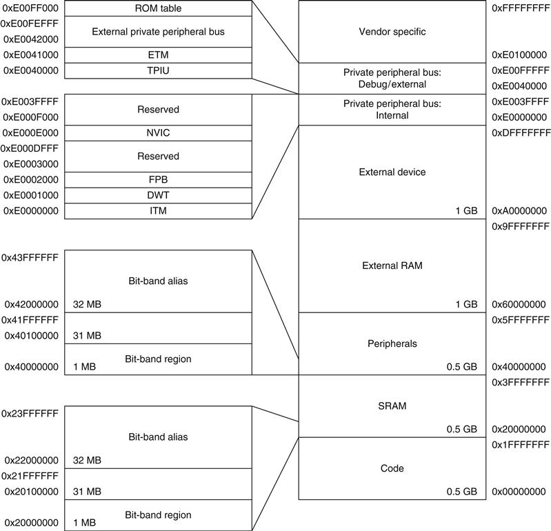
Some of the memory locations are allocated for private peripherals such as debugging components. They are located in the private peripheral memory region. These debugging components include the following:
• Fetch Patch and Breakpoint Unit (FPB)
• Data Watchpoint and Trace Unit (DWT)
• Instrumentation Trace Macrocell (ITM)
• Embedded Trace Macrocell (ETM)
The details of these components are discussed in later chapters on debugging features.
The Cortex-M3 processor has a total of 4 GB of address space. Program code can be located in the code region, the Static Random Access Memory (SRAM) region, or the external RAM region. However, it is best to put the program code in the code region because with this arrangement, the instruction fetches and data accesses are carried out simultaneously on two separate bus interfaces.
The SRAM memory range is for connecting internal SRAM. Access to this region is carried out via the system interface bus. In this region, a 32-MB range is defined as a bit-band alias. Within the 32-bit‑band alias memory range, each word address represents a single bit in the 1-MB bit-band region. A data write access to this bit-band alias memory range will be converted to an atomic READ-MODIFY-WRITE operation to the bit-band region so as to allow a program to set or clear individual data bits in the memory. The bit-band operation applies only to data accesses not instruction fetches. By putting Boolean information (single bits) in the bit-band region, we can pack multiple Boolean data in a single word while still allowing them to be accessible individually via bit-band alias, thus saving memory space without the need for handling READ-MODIFY-WRITE in software. More details on bit-band alias can be found later in this chapter.
Another 0.5-GB block of address range is allocated to on-chip peripherals. Similar to the SRAM region, this region supports bit-band alias and is accessed via the system bus interface. However, instruction execution in this region is not allowed. The bit-band support in the peripheral region makes it easy to access or change control and status bits of peripherals, making it easier to program peripheral control.
Two slots of 1-GB memory space are allocated for external RAM and external devices. The difference between the two is that program execution in the external device region is not allowed, and there are some differences with the caching behaviors.
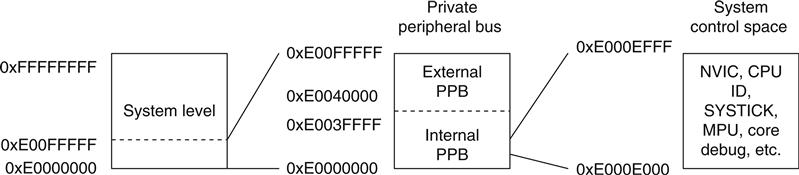
The last 0.5-GB memory is for the system-level components, internal peripheral buses, external peripheral bus, and vendor-specific system peripherals. There are two segments of the private peripheral bus (PPB):
• Advanced High-Performance Bus (AHB) PPB, for Cortex-M3 internal AHB peripherals only; this includes NVIC, FPB, DWT, and ITM
• Advance Peripheral Bus (APB) PPB, for Cortex-M3 internal APB devices as well as external peripherals (external to the Cortex-M3 processor); the Cortex-M3 allows chip vendors to add additional on-chip APB peripherals on this private peripheral bus via an APB interface
The NVIC is located in a memory region called the system control space (SCS) (see Figure 5.2). Besides providing interrupt control features, this region also provides the control registers for SYSTICK, MPU, and code debugging control.
The remaining unused vendor-specific memory range can be accessed via the system bus interface. However, instruction execution in this region is not allowed.
The Cortex-M3 processor also comes with an optional MPU. Chip manufacturers can decide whether to include the MPU in their products.
What we have shown in the memory map is merely a template; individual semiconductor vendors provide detailed memory maps including the actual location and size of ROM, RAM, and peripheral memory locations.
5.3 Memory Access Attributes
The memory map shows what is included in each memory region. Aside from decoding which memory block or device is accessed, the memory map also defines the memory attributes of the access. The memory attributes you can find in the Cortex-M3 processor include the following:
• Bufferable: Write to memory can be carried out by a write buffer while the processor continues on next instruction execution.
• Cacheable: Data obtained from memory read can be copied to a memory cache so that next time it is accessed the value can be obtained from the cache to speed up the program execution.
• Executable: The processor can fetch and execute program code from this memory region.
• Sharable: Data in this memory region could be shared by multiple bus masters. Memory system needs to ensure coherency of data between different bus masters in shareable memory region.
The Cortex-M3 bus interfaces output the memory access attributes information to the memory system for each instruction and data transfer. The default memory attribute settings can be overridden if MPU is present and the MPU region configurations are programmed differently from the default. Though the Cortex-M3 processor does not have a cache memory or cache controller, a cache unit can be added on the microcontroller which can use the memory attribute information to define the memory access behaviors. In addition, the cache attributes might also affect the operation of memory controllers for on-chip memory and off-chip memory, depending on the memory controllers used by the chip manufacturers.
The memory access attributes for each memory region are as follows:
• Code memory region (0x00000000–0x1FFFFFFF): This region is executable, and the cache attribute is write through (WT). You can put data memory in this region as well. If data operations are carried out for this region, they will take place via the data bus interface. Write transfers to this region are bufferable.
• SRAM memory region (0x20000000–0x3FFFFFFF): This region is intended for on-chip RAM. Write transfers to this region are bufferable, and the cache attribute is write back, write allocated (WB-WA). This region is executable, so you can copy program code here and execute it.
• Peripheral region (0x40000000–0x5FFFFFFF): This region is intended for peripherals. The accesses are noncacheable. You cannot execute instruction code in this region (Execute Never, or XN in ARM documentation, such as the Cortex-M3 TRM).
• External RAM region (0x60000000–0x7FFFFFFF): This region is intended for either on-chip or off-chip memory. The accesses are cacheable (WB-WA), and you can execute code in this region.
• External RAM region (0x80000000–0x9FFFFFFF): This region is intended for either on-chip or off-chip memory. The accesses are cacheable (WT), and you can execute code in this region.
• External devices (0xA0000000–0xBFFFFFFF): This region is intended for external devices and/or shared memory that needs ordering/nonbuffered accesses. It is also a nonexecutable region.
• External devices (0xC0000000–0xDFFFFFFF): This region is intended for external devices and/or shared memory that needs ordering/nonbuffered accesses. It is also a nonexecutable region.
• System region (0xE0000000–0xFFFFFFFF): This region is for private peripherals and vendor-specific devices. It is nonexecutable. For the PPB memory range, the accesses are strongly ordered (noncacheable, nonbufferable). For the vendor-specific memory region, the accesses are bufferable and noncacheable.
Note that from Revision 1 of the Cortex-M3, the code region memory attribute export to external memory system is hardwired to cacheable and nonbufferable. This cannot be overridden by MPU configuration. This update only affects the memory system outside the processor (e.g., level 2 cache and certain types of memory controllers with cache features). Within the processor, the internal write buffer can still be used for write transfers accessing the code region.
5.4 Default Memory Access Permissions
The Cortex-M3 memory map has a default configuration for memory access permissions. This prevents user programs (non-privileged) from accessing system control memory spaces such as the NVIC. The default memory access permission is used when either no MPU is present or MPU is present but disabled.
If MPU is present and enabled, the access permission in the MPU setup will determine whether user accesses are allowed.
The default memory access permissions are shown in Table 5.1.
Table 5.1
Default Memory Access Permissions
| Memory Region | Address | Access in User Program |
| Vendor specific | 0xE0100000–0xFFFFFFFF | Full access |
| ROM table | 0xE00FF000–0xE00FFFFF | Blocked; user access results in bus fault |
| External PPB | 0xE0042000–0xE00FEFFF | Blocked; user access results in bus fault |
| ETM | 0xE0041000–0xE0041FFF | Blocked; user access results in bus fault |
| TPIU | 0xE0040000–0xE0040FFF | Blocked; user access results in bus fault |
| Internal PPB | 0xE000F000–0xE003FFFF | Blocked; user access results in bus fault |
| NVIC | 0xE000E000–0xE000EFFF | Blocked; user access results in bus fault, except Software Trigger Interrupt Register that can be programmed to allow user accesses |
| FPB | 0xE0002000–0xE0003FFF | Blocked; user access results in bus fault |
| DWT | 0xE0001000–0xE0001FFF | Blocked; user access results in bus fault |
| ITM | 0xE0000000–0xE0000FFF | Read allowed; write ignored except for stimulus ports with user access enabled |
| External device | 0xA0000000–0xDFFFFFFF | Full access |
| External RAM | 0x60000000–0x9FFFFFFF | Full access |
| Peripheral | 0x40000000–0x5FFFFFFF | Full access |
| SRAM | 0x20000000–0x3FFFFFFF | Full access |
| Code | 0x00000000–0x1FFFFFFF | Full access |
When a user access is blocked, the fault exception takes place immediately.
5.5 Bit-Band Operations
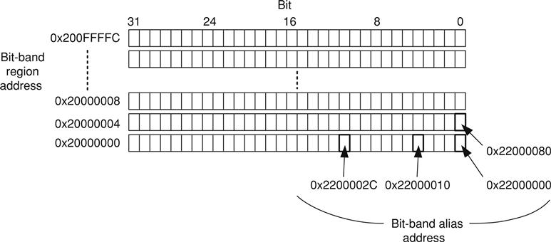
Bit-band operation support allows a single load/store operation to access (read/write) to a single data bit. In the Cortex-M3, this is supported in two predefined memory regions called bit-band regions. One of them is located in the first 1 MB of the SRAM region, and the other is located in the first 1 MB of the peripheral region. These two memory regions can be accessed like normal memory, but they can also be accessed via a separate memory region called the bit-band alias (see Figure 5.3). When the bit-band alias address is used, each individual bit can be accessed separately in the least significant bit (LSB) of each word-aligned address.
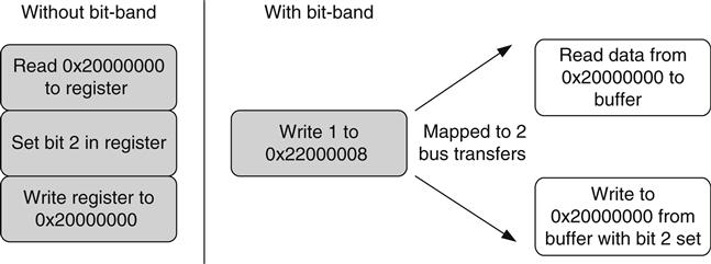
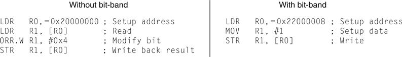
For example, to set bit 2 in word data in address 0x20000000, instead of using three instructions to read the data, set the bit, and then write back the result, this task can be carried out by a single instruction (see Figure 5.4). The assembler sequence for these two cases could be like the one shown in Figure 5.5.
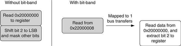
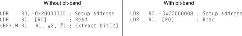
Similarly, bit-band support can simplify application code if we need to read a bit in a memory location. For example, if we need to determine bit 2 of address 0x20000000, we use the steps outlined in Figure 5.6. The assembler sequence for these two cases could be like the one shown in Figure 5.7.
Bit-band operation is not a new idea; in fact, a similar feature has existed for more than 30 years on 8-bit microcontrollers such as the 8051. Although the Cortex-M3 does not have special instructions for bit operation, special memory regions are defined so that data accesses to these regions are automatically converted into bit-band operations.
Note that the Cortex-M3 uses the following terms for the bit-band memory addresses:
• Bit-band region: This is a memory address region that supports bit-band operation.
• Bit-band alias: Access to the bit-band alias will cause an access (a bit-band operation) to the bit-band region. (Note: A memory remapping is performed.)
Within the bit-band region, each word is represented by an LSB of 32 words in the bit-band alias address range. What actually happens is that when the bit-band alias address is accessed, the address is remapped into a bit-band address. For read operations, the word is read and the chosen bit location is shifted to the LSB of the read return data. For write operations, the written bit data are shifted to the required bit position, and a READ-MODIFY-WRITE is performed.
There are two regions of memory for bit-band operations:
For the SRAM memory region, the remapping of the bit-band alias is shown in Table 5.2.
Table 5.2
Remapping of Bit-Band Addresses in SRAM Region
| Bit-Band Region | Aliased Equivalent |
| 0x20000000 bit[0] | 0x22000000 bit[0] |
| 0x20000000 bit[1] | 0x22000004 bit[0] |
| 0x20000000 bit[2] | 0x22000008 bit[0] |
| … | … |
| 0x20000000 bit[31] | 0x2200007C bit[0] |
| 0x20000004 bit[0] | 0x22000080 bit[0] |
| … | … |
| 0x20000004 bit[31] | 0x220000FC bit[0] |
| … | … |
| 0x200FFFFC bit[31] | 0x23FFFFFC bit[0] |
Similarly, the bit-band region of the peripheral memory region can be accessed via bit-band aliased addresses, as shown in Table 5.3.
Table 5.3
Remapping of Bit-Band Addresses in Peripheral Memory Region
| Bit-Band Region | Aliased Equivalent |
| 0x40000000 bit[0] | 0x42000000 bit[0] |
| 0x40000000 bit[1] | 0x42000004 bit[0] |
| 0x40000000 bit[2] | 0x42000008 bit[0] |
| … | … |
| 0x40000000 bit[31] | 0x4200007C bit[0] |
| 0x40000004 bit[0] | 0x42000080 bit[0] |
| … | … |
| 0x40000004 bit[31] | 0x420000FC bit[0] |
| … | … |
| 0x400FFFFC bit[31] | 0x43FFFFFC bit[0] |
1. Set address 0x20000000 to a value of 0x3355AACC.
2. Read address 0x22000008. This read access is remapped into read access to 0x20000000. The return value is 1 (bit[2] of 0x3355AACC).
3. Write 0x0 to 0x22000008. This write access is remapped into a READ-MODIFY-WRITE to 0x20000000. The value 0x3355AACC is read from memory, bit 2 is cleared, and a result of 0x3355AAC8 is written back to address 0x20000000.
4. Now, read 0x20000000. That gives you a return value of 0x3355AAC8 (bit[2] cleared).
When you access bit-band alias addresses, only the LSB (bit[0]) in the data is used. In addition, accesses to the bit-band alias region should not be unaligned. If an unaligned access is carried out to bit-band alias address range, the result is unpredictable.
5.5.1 Advantages of Bit-Band Operations
So, what are the uses of bit-band operations? We can use them to, for example, implement serial data transfers in general-purpose input/output (GPIO) ports to serial devices. The application code can be implemented easily because access to serial data and clock signals can be separated.
Bit-band operation can also be used to simplify branch decisions. For example, if a branch should be carried out based on 1 single bit in a status register in a peripheral, instead of
you can simplify the operations to
Besides providing faster bit operations with fewer instructions, the bit-band feature in the Cortex-M3 is also essential for situations in which resources are being shared by more than one process. One of the most important advantages or properties of a bit-band operation is that it is atomic. In other words, the READ-MODIFY-WRITE sequence cannot be interrupted by other bus activities. Without this behavior in, for example, using a software READ-MODIFY-WRITE sequence, the following problem can occur: consider a simple output port with bit 0 used by a main program and bit 1 used by an interrupt handler. A software-based READ-MODIFY-WRITE operation can cause data conflicts, as shown in Figure 5.8.

With the Cortex-M3 bit-band feature, this kind of race condition can be avoided because the READ-MODIFY-WRITE is carried out at the hardware level and is atomic (the two transfers cannot be pulled apart) and interrupts cannot take place between them (see Figure 5.9).

Similar issues can be found in multitasking systems. For example, if bit 0 of the output port is used by Process A and bit 1 is used by Process B, a data conflict can occur in software-based READ-MODIFY-WRITE (see Figure 5.10).

Again, the bit-band feature can ensure that bit accesses from each task are separated so that no data conflicts occur (see Figure 5.11).

Besides I/O functions, the bit-band feature can be used for storing and handling Boolean data in the SRAM region. For example, multiple Boolean variables can be packed into one single memory location to save memory space, whereas the access to each bit is still completely separated when the access is carried out via the bit-band alias address range.
For system-on-chip (SoC) designers designing a bit-band-capable device, the device's memory address should be located within the bit-band memory, and the lock (HMASTLOCK) signal from the AHB interface must be checked to make sure that writable register contents will not be changed except by the bus when a locked transfer is carried out.
5.5.2 Bit-Band Operation of Different Data Sizes
Bit-band operation is not limited to word transfers. It can be carried out as byte transfers or half word transfers as well. For example, when a byte access instruction (LDRB/STRB) is used to access a bit-band alias address range, the accesses generated to the bit-band region will be in byte size. The same applies to half word transfers (LDRH/STRH). When you use nonword transfers to bit-band alias addresses, the address value should still be word aligned.
5.5.3 Bit-Band Operations in C Programs
There is no native support of bit-band operation in most C compilers. For example, C compilers do not understand that the same memory can be accessed using two different addresses, and they do not know that accesses to the bit-band alias will only access the LSB of the memory location. To use the bit-band feature in C, the simplest solution is to separately declare the address and the bit-band alias of a memory location. For example:
#define DEVICE_REG0 *((volatile unsigned long *) (0x40000000))
#define DEVICE_REG0_BIT0 *((volatile unsigned long *) (0x42000000))
#define DEVICE_REG0_BIT1 *((volatile unsigned long *) (0x42000004))
...
DEVICE_REG0 = 0xAB; // Accessing the hardware register by normal
// address
...
DEVICE_REG0 = DEVICE_REG0 | 0x2; // Setting bit 1 without using
// bitband feature
...
DEVICE_REG0_BIT1 = 0x1; // Setting bit 1 using bitband feature
// via the bit band alias address
It is also possible to develop C macros to make accessing the bit-band alias easier. For example, we could set up one macro to convert the bit-band address and the bit number into the bit-band alias address and set up another macro to access the memory location by taking the address value as a pointer:
// Convert bit band address and bit number into
// bit band alias address
#define BITBAND(addr,bitnum) ((addr & 0xF0000000)+0x2000000+((addr & 0xFFFFF)<<5)+(bitnum <<2))
// Convert the address as a pointer
#define MEM_ADDR(addr) *((volatile unsigned long *) (addr))
Based on the previous example, we rewrite the code as follows:
#define DEVICE_REG0 0x40000000
#define BITBAND(addr,bitnum) ((addr & 0xF0000000)+0x02000000+((addr & 0xFFFFF)<<5)+(bitnum<<2))
#define MEM_ADDR(addr) *((volatile unsigned long *) (addr))
...
MEM_ADDR(DEVICE_REG0) = 0xAB; // Accessing the hardware
// register by normal address
...
// Setting bit 1 without using bitband feature
MEM_ADDR(DEVICE_REG0) = MEM_ADDR(DEVICE_REG0) | 0x2;
...
// Setting bit 1 with using bitband feature
MEM_ADDR(BITBAND(DEVICE_REG0,1)) = 0x1;
Note that when the bit-band feature is used, the variables being accessed might need to be declared as volatile. The C compilers do not know that the same data could be accessed in two different addresses, so the volatile property is used to ensure that each time a variable is accessed, the memory location is accessed instead of a local copy of the data inside the processor.
Starting from ARM RealView Development Suite version 4.0 and Keil MDK-ARM 3.80, bit band support is provided by __attribute__((bitband)) language extension and __bitband command line option (see reference 6). You can find further examples of bit-band accesses with C macros using ARM RealView Compiler Tools in the ARM Application Note 179 [Ref. 7].
5.6 Unaligned Transfers
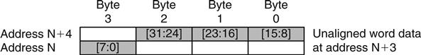
The Cortex-M3 supports unaligned transfers on single accesses. Data memory accesses can be defined as aligned or unaligned. Traditionally, ARM processors (such as the ARM7/ARM9/ARM10) allow only aligned transfers. That means in accessing memory, a word transfer must have address bit[1] and bit[0] equal to 0, and a half word transfer must have address bit[0] equal to 0. For example, word data can be located at 0x1000 or 0x1004, but it cannot be located in 0x1001, 0x1002, or 0x1003. For half word data, the address can be 0x1000 or 0x1002, but it cannot be 0x1001.
So, what does an unaligned transfer look like? Figures 5.12 through 5.16 show some examples. Assuming that the memory infrastructure is 32-bit (4 bytes) wide, an unaligned transfer can be any word size read/write such that the address is not a multiple of 4, as shown in Figures 5.12–5.14, or when the transfer is in half word size, and the address is not a multiple of 2, as shown in Figures 5.15 and 5.16.


All the byte-size transfers are aligned on the Cortex-M3 because the minimum address step is 1 byte.
In the Cortex-M3, unaligned transfers are supported in normal memory accesses (such as LDR, LDRH, STR, and STRH instructions). There are a number of limitations:
• Unaligned transfers are not supported in Load/Store multiple instructions.
• Stack operations (PUSH/POP) must be aligned.
• Exclusive accesses (such as LDREX or STREX) must be aligned; otherwise, a fault exception (usage fault) will be triggered.
• Unaligned transfers are not supported in bit-band operations. Results will be unpredictable if you attempt to do so.
When unaligned transfers are used, they are actually converted into multiple aligned transfers by the processor's bus interface unit. This conversion is transparent, so application programmers do not have to worry about it. However, when an unaligned transfer takes place, it is broken into separate transfers, and as a result, it takes more clock cycles for a single data access and might not be good for situations in which high performance is required. To get the best performance, it's worth making sure that data are aligned properly.
It is also possible to set up the NVIC so that an exception is triggered when an unaligned transfer takes place. This is done by setting the UNALIGN_TRP (unaligned trap) bit in the configuration control register in the NVIC (0xE000ED14). In this way, the Cortex-M3 generates usage fault exceptions when unaligned transfers take place. This is useful during software development to test whether an application produces unaligned transfers.
5.7 Exclusive Accesses
You might have noticed that the Cortex-M3 has no SWP instruction (swap), which was used for semaphore operations in traditional ARM processors like ARM7TDMI. This is now being replaced by exclusive access operations. Exclusive accesses were first supported in architecture v6 (for example, in the ARM1136).
Semaphores are commonly used for allocating shared resources to applications. When a shared resource can only service one client or application processor, we also call it Mutual Exclusion (MUTEX). In such cases, when a resource is being used by one process, it is locked to that process and cannot serve another process until the lock is released. To set up a MUTEX semaphore, a memory location is defined as the lock flag to indicate whether a shared resource is locked by a process. When a process or application wants to use the resource, it needs to check whether the resource has been locked first. If it is not being used, it can set the lock flag to indicate that the resource is now locked. In traditional ARM processors, the access to the lock flag is carried out by the SWP instruction. It allows the lock flag read and write to be atomic, preventing the resource from being locked by two processes at the same time.
In newer ARM processors, the read/write access can be carried out on separated buses. In such situations, the SWP instructions can no longer be used to make the memory access atomic because the read and write in a locked transfer sequence must be on the same bus. Therefore, the locked transfers are replaced by exclusive accesses. The concept of exclusive access operation is quite simple but different from SWP; it allows the possibility that the memory location for a semaphore could be accessed by another bus master or another process running on the same processor (see Figure 5.17).
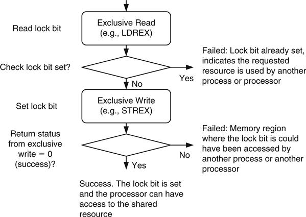
To allow exclusive access to work properly in a multiple processor environment, an additional hardware called “exclusive access monitor” is required. This monitor checks the transfers toward shared address locations and replies to the processor if an exclusive access is success. The processor bus interface also provides additional control signals1 to this monitor to indicate if the transfer is an exclusive access.
If the memory device has been accessed by another bus master between the exclusive read and the exclusive write, the exclusive access monitor will flag an exclusive failed through the bus system when the processor attempts the exclusive write. This will cause the return status of the exclusive write to be 1. In the case of failed exclusive write, the exclusive access monitor also blocks the write transfer from getting to the exclusive access address.
Exclusive access instructions in the Cortex-M3 include LDREX (word), LDREXB (byte), LDREXH (half word), STREX (word), STREXB (byte), and STREXH (half word). A simple example of the syntax is as follows:
LDREX <Rxf>, [Rn, #offset]
STREX <Rd>, <Rxf>, [Rn, #offset]
Where Rd is the return status of the exclusive write (0 = success and 1 = failure). Example code for exclusive accesses can be found in Chapter 10. You can also access exclusive access instructions in C using intrinsic functions provided in Cortex Microcontroller Software Interface Standard (CMSIS) compliant device driver libraries from microcontroller vendors: __LDREX, __LEDEXH, __LDREXB, __STREX, __STREXH, __STREXB. More details of these functions are covered in Appendix G.
When exclusive accesses are used, the internal write buffers in the Cortex-M3 bus interface will be bypassed, even when the MPU defines the region as bufferable. This ensures that semaphore information on the physical memory is always up to date and coherent between bus masters. SoC designers using Cortex-M3 on multiprocessor systems should ensure that the memory system enforces data coherency when exclusive transfers occur.
5.8 Endian Mode
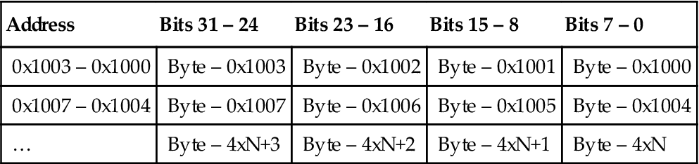
The Cortex-M3 supports both little endian and big endian modes. However, the supported memory type also depends on the design of the rest of the microcontroller (bus connections, memory controllers, peripherals, and so on). Make sure that you check your microcontroller datasheets in detail before developing your software. In most cases, Cortex-M3-based microcontrollers will be little endian. With little endian mode, the first byte of a word size data is stored in the least significant byte of the 32-bit memory location (see Table 5.4).
Table 5.4
The Cortex-M3 Little Endian Memory View Example
| Address | Bits 31 – 24 | Bits 23 – 16 | Bits 15 – 8 | Bits 7 – 0 |
| 0x1003 – 0x1000 | Byte – 0x1003 | Byte – 0x1002 | Byte – 0x1001 | Byte – 0x1000 |
| 0x1007 – 0x1004 | Byte – 0x1007 | Byte – 0x1006 | Byte – 0x1005 | Byte – 0x1004 |
| … | Byte – 4xN+3 | Byte – 4xN+2 | Byte – 4xN+1 | Byte – 4xN |
There are some microcontrollers that use big endian mode. In such a case, the first byte of a word size data is stored in the most significant byte of the 32-bit address memory location (see Table 5.5).
Table 5.5
The Cortex-M3 Big Endian Memory View Example
| Address | Bits 31 – 24 | Bits 23 – 16 | Bits 15 – 8 | Bits 7 – 0 |
| 0x1003 – 0x1000 | Byte – 0x1000 | Byte – 0x1001 | Byte – 0x1002 | Byte – 0x1003 |
| 0x1007 – 0x1004 | Byte – 0x1004 | Byte – 0x1005 | Byte – 0x1006 | Byte – 0x1007 |
| … | Byte – 4xN | Byte – 4xN+1 | Byte – 4xN+2 | Byte – 4xN+3 |
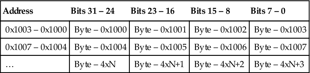
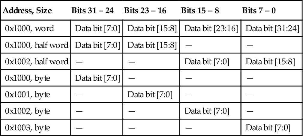
The definition of big endian in the Cortex-M3 is different from the ARM7. In the ARM7TDMI, the big endian scheme is called word-invariant big endian, also referred as BE-32 in ARM documentation, whereas in the Cortex-M3, the big endian scheme is called byte-invariant big endian, also referred as BE-8 (byte-invariant big endian is supported on ARM architecture v6 and v7). The memory view of both schemes is the same, but the byte lane usage on the bus interface during data transfers is different (see Tables 5.6 and 5.7).
Table 5.6
The Cortex-M3 (Byte-Invariant Big Endian, BE-8)—Data on the AHB Bus
| Address, Size | Bits 31 – 24 | Bits 23 – 16 | Bits 15 – 8 | Bits 7 – 0 |
| 0x1000, word | Data bit [7:0] | Data bit [15:8] | Data bit [23:16] | Data bit [31:24] |
| 0x1000, half word | — | — | Data bit [7:0] | Data bit [15:8] |
| 0x1002, half word | Data bit [7:0] | Data bit [15:8] | — | — |
| 0x1000, byte | — | — | — | Data bit [7:0] |
| 0x1001, byte | — | — | Data bit [7:0] | — |
| 0x1002, byte | — | Data bit [7:0] | — | — |
| 0x1003, byte | Data bit [7:0] | — | — | — |
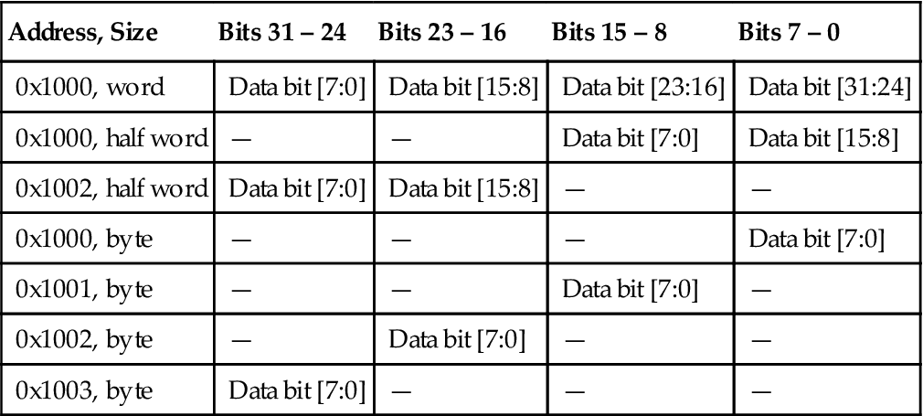
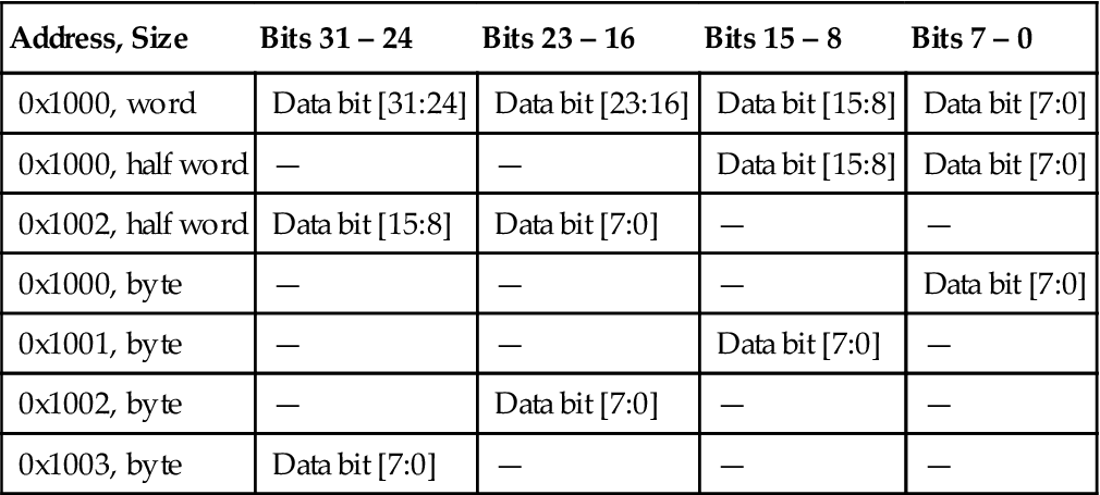
Table 5.7
ARM7TDMI (Word-Invariant Big Endian, BE-32)—Data on the AHB Bus
| Address, Size | Bits 31 – 24 | Bits 23 – 16 | Bits 15 – 8 | Bits 7 – 0 |
| 0x1000, word | Data bit [7:0] | Data bit [15:8] | Data bit [23:16] | Data bit [31:24] |
| 0x1000, half word | Data bit [7:0] | Data bit [15:8] | — | — |
| 0x1002, half word | — | — | Data bit [7:0] | Data bit [15:8] |
| 0x1000, byte | Data bit [7:0] | — | — | — |
| 0x1001, byte | — | Data bit [7:0] | — | — |
| 0x1002, byte | — | — | Data bit [7:0] | — |
| 0x1003, byte | — | — | — | Data bit [7:0] |
Note that the data transfer on the AHB bus in BE-8 mode uses the same data byte lanes as in little endian. However, the data byte inside the half word or word data is reversely ordered compared to little endian (see Table 5.8).
Table 5.8
The Cortex-M3 Little Endian—Data on the AHB Bus
| Address, Size | Bits 31 – 24 | Bits 23 – 16 | Bits 15 – 8 | Bits 7 – 0 |
| 0x1000, word | Data bit [31:24] | Data bit [23:16] | Data bit [15:8] | Data bit [7:0] |
| 0x1000, half word | — | — | Data bit [15:8] | Data bit [7:0] |
| 0x1002, half word | Data bit [15:8] | Data bit [7:0] | — | — |
| 0x1000, byte | — | — | — | Data bit [7:0] |
| 0x1001, byte | — | — | Data bit [7:0] | — |
| 0x1002, byte | — | Data bit [7:0] | — | — |
| 0x1003, byte | Data bit [7:0] | — | — | — |
In the Cortex-M3 processor, the endian mode is set when the processor exits reset. The endian mode cannot be changed afterward. (There is no dynamic endian switching, and the SETEND instruction is not supported.) Instruction fetches are always in little endian as are data accesses in the system control memory space (such as NVIC and FPB) and the external PPB memory range (memory range from 0xE0000000 to 0xE00FFFFF is always little endian).
In case your SoC does not support big endian but one or some of the peripherals you are using contain big endian data, you can easily convert the data between little endian and big endian using some of the data type conversion instructions in the Cortex-M3. For example, REV and REV16 are very useful for this kind of conversion.