Debugging Components
Publisher Summary
This chapter focuses on a number of debugging components used to provide debugging features such as breakpoint, watchpoint, Flash Patch, and trace that the Cortex™-M3 processor comes with, all of which can be programmed through the Cortex-M3 Private Peripheral Bus. The chapter discusses the trace system that is based on CoreSight architecture—the Data Watchpoint and Trace (DWT) components and their debugging functionalities; the Instrumentation Trace Macrocell (ITM), a control register for controlling the enabling of individual features; the hardware trace with ITM and DWT; and the Embedded Trace Macrocell that is used for providing instruction traces. The chapter describes other trace components as well, which include the Trace Port Interface Unit and the Flash Patch and Breakpoint unit. It explains the Advanced High-Performance Bus Access Port (AHB-AP), a bridge between the debug interface module and the Cortex-M3 memory system, exploring three registers in the AHB-AP—the CSW register that can control the transfers, the TAR register that is used to specify the transfer address, and the DRW register that is used to carry out the data transfer operation. The ROM table, used to allow auto detection of debug components inside a Cortex-M3 chip, is also explored.
16.1 Introduction
The Cortex™-M3 processor comes with a number of debugging components used to provide debugging features such as breakpoint, watchpoint, Flash Patch, and trace. If you are an application developer, there might be a chance that you'll never need to know the details about these debugging components because they are normally used only by debugger tools. This chapter will introduce you to the basics of each debug component. If you want to know the details about things such as the actual programmer's model, refer to the Cortex-M3 Technical Reference Manual [Ref. 1].
All the debug trace components, as well as the Flash Patch and Breakpoint (FPB), can be programmed through the Cortex-M3 Private Peripheral Bus (PPB). In most cases, the components will only be programmed by the debugging host. It is not recommended for applications to try accessing the debug components (except stimulus port registers in the Instrumentation Trace Macrocell [ITM]) because this could interfere with the debugger's operation.
16.1.1 The Trace System in the Cortex-M3
The Cortex-M3 trace system is based on the CoreSight architecture. Trace results are generated in the form of packets, which can be of various lengths (in terms of number of bytes). The trace components transfer the packets using Advanced Trace Bus (ATB) to the Trace Port Interface Unit (TPIU), which formats the packets into Trace Interface Protocol. The data is then captured by an external trace capture device such as a Trace Port Analyzer (TPA), as shown in Figure 16.1.

There are up to three trace sources in a standard Cortex-M3 processor: Embedded Trace Macrocell (ETM), ITM, and Data Watchpoint and Trace (DWT). Note that the ETM in the Cortex-M3 is optional, so some Cortex-M3 products do not have instruction trace capability. During operation, each trace source is assigned a 7-bit ATB Trace ID value (ATID), which is transferred along the trace packets during merging in the ATB so that the packets can be separated back into multiple trace streams when they reach the debug host.
Unlike many other standard CoreSight components, the debug components in the Cortex-M3 processor include the functionality of merging ATB streams, whereas in standard CoreSight systems, ATB packet merger, called ATB funnel, is a separate block.
Before using the trace system, the Trace Enable (TRCENA) bit in the Debug Exception and Monitor Control register (DEMCR) must be set to 1 (see Table 15.2 or D.38). Otherwise, the trace system will be disabled. In normal operations that do not require tracing, clearing the TRCENA bit can disable some of the trace logic and reduce the power consumption.
16.2 Trace Components: DWT
The DWT has a number of debugging functionalities:
1 It has four comparators, each of which can be configured as follows:
a Hardware watch point (generates a watch point event to the processor to invoke debug modes such as halt or debug monitor)
b ETM trigger (causes the ETM to emit a trigger packet in the instruction trace stream)
d Data address sampler trigger
The first comparator can also be used to compare against the clock cycle counter (CYCCNT) instead of comparing with a data address.
2 Counters for counting the following:
When used as a hardware watchpoint or ETM trigger, the comparator can be programmed to compare either data addresses or program counters. When programmed as other functions, it compares the data addresses.
Each of the comparators has three corresponding registers, which are as follows:
The COMP register is a 32-bit register that the data address (or program counter value, or CYCCNT) compares to. The MASK register determines whether any bit in the data address will be ignored during the compare (see Table 16.1).
Table 16.1
Encoding of the DWT Mask Registers
| MASK | Ignore Bit |
| 0 | All bits are compared |
| 1 | Ignore bit [0] |
| 2 | Ignore bit [1:0] |
| 3 | Ignore bit [2:0] |
| … | … |
| 15 | Ignore bit [14:0] |
By using the mask register, it is possible to trace data access in an address range of 32 KB maximum size. However, because of the limited first in/first out (FIFO) size in the DWT and the ITM, it is not practical to trace lots of data transfers as this will cause trace overflow and result in loss of trace data.
The comparator's FUNCTION register determines its function. To avoid unexpected behavior, the MASK register and the COMP register should be programmed before this register is set. If the comparator's function is to be changed, you should disable the comparator by setting FUNCTION to 0 (disable), then program the MASK and COMP registers, and then enable the FUNCTION register in the last step.
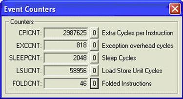
The rest of the DWT counters are typically used for profiling the application codes. They can be programmed to emit events (in the form of trace packets) when the counter overflows. One typical application is to use the CYCCNT register to count the number of clock cycles required for a specific task, for benchmarking purposes.
For example, the Keil μVision development tool can use these profiling counters to generate statistical information (see Figure 16.2). These counters trigger event packets to be generated and are collected by the debugger through the Serial Wire Viewer (SWV) output.
The TRCENA bit in the DEMCR must be set to 1 before the DWT is used. If the DWT is being used to generate a trace, the DWT enable (DWTEN) bit in the ITM control register should also be enabled.
16.3 Trace Components: ITM
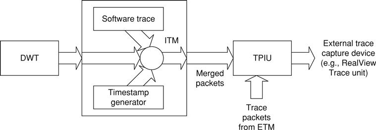
The ITM has the following functionalities, as shown in Figure 16.3:
• Software can directly write console messages to ITM stimulus ports and output them as trace data.
• The DWT can generate trace packets and output them through the ITM.
• The ITM can generate timestamp packets that are inserted into a trace stream to help the debugger find out the timing of events.
Because the ITM uses a trace port to output data, if the microcontroller or system-on-chip (SoC) does not have TPIU support, the traced information cannot be output. Therefore, it is necessary to check whether the microcontroller or SoC has all the required features before you use the ITM. In the worst case, if these features are not available, you can still use semihosting via the Nested Vectored Interrupt Controller (NVIC) debug register (supported by ARM RealView Debugger) or a universal asynchronous receiver/transmitter (UART) to output console messages.
To use the ITM, the TRCENA bit in the DEMCR must be set to 1. Otherwise, the ITM will be disabled and ITM registers cannot be accessed.
In addition, there is also a lock register in the ITM. You need to write the access key 0xC5ACCE55 (CoreSight ACCESS) to this register before programming the ITM. Otherwise, all write operations to the ITM will be ignored.
Finally, the ITM itself is another control register to control the enabling of individual features. The control register also contains the ATID field, which is an ID value for the ITM in the ATB. This ID value must be unique from the IDs for other trace sources, so that the debug host receiving the trace packet can separate the ITM's trace packets from other trace packets.
16.3.1 Software Trace with the ITM
One of the main uses of the ITM is to support debug message output (such as printf). The ITM contains 32 stimulus ports, allowing different software processes to output to different ports, and the messages can be separated later at the debug host. Each port can be enabled or disabled by the Trace Enable register and can be programmed (in groups of eight ports) to allow or disallow user processes to write to it.
Unlike UART-based text output, using the ITM to output does not cause much delay for the application. A FIFO buffer is used inside the ITM, so writing output messages can be buffered. However, it is still necessary to check whether the FIFO is full before you write to it.
The output messages can be collected at the trace port interface or the Serial Wire Viewer interface (SWV) on the TPIU. There is no need to remove code that generates the debug messages from the final code because if the TRCENA control bit is low, the ITM will be inactive and debug messages will not be output. You can also switch on the output message in a “live” system and use the Trace Enable register in the ITM to limit which ports are enabled so that only some of the messages can be output.
For example, the Keil μVision development tool can collect and display the text output using the ITM viewer shown in Figure 16.4.

16.3.2 Hardware Trace with ITM and DWT
The ITM is used in output of hardware trace packets. The packets are generated from the DWT, and the ITM acts as a trace packet merging unit. To use DWT trace, you need to enable the DWTEN bit in the ITM control register; the rest of the DWT trace settings still need to be programmed at the DWT.
16.3.3 ITM Timestamp
ITM has a timestamp feature that allows trace capture tools to find out timing information by inserting delta timestamp packets into the traces when a new trace packet enters the FIFO inside the ITM. The timestamp packet is also generated when the timestamp counter overflows.
The timestamp packets provide the time difference (delta) with previous events. Using the delta timestamp packets, the trace capture tools can then establish the timing of when each packet is generated, and hence reconstruct the timing of various debug events.
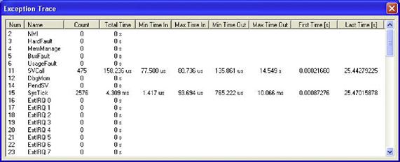
Combining the trace functionality of DWT and ITM, we can collect a lot of useful information. For example, the exception trace windows in the Keil μVision development tool can tell you what exceptions have been carried out and how much time was spend on the exceptions, as shown in Figure 16.5.
16.4 Trace Components: ETM
The ETM block is used for providing instruction traces. It is optional and might not be available on some Cortex-M3 products. When it is enabled and when the trace operation starts, it generates instruction trace packets. A FIFO buffer is provided in the ETM to allow enough time for the trace stream to be captured.
To reduce the amount of data generated by the ETM, it does not always output exactly what address the processor has reached/executed. It usually outputs information about program flow and outputs full addresses only if needed (e.g., if a branch has taken place). Because the debugging host should have a copy of the binary image, it can then reconstruct the instruction sequence the processor has carried out.
The ETM also interacts with other debugging components such as the DWT. The comparators in the DWT can be used to generate trigger events in the ETM or to control the trace start/stop.
Unlike the ETM in traditional ARM processors, the Cortex-M3 ETM does not have its own address comparators, because the DWT can carry out the comparison for ETM. Furthermore, because the data trace functionality is carried out by the DWT, the ETM design in the Cortex-M3 is quite different from traditional ETM for other ARM cores.
To use the ETM in the Cortex-M3, the following setup is required (handled by debug tools):
1 The TRCENA bit in the DEMCR must be set to 1 (refer to Table 15.2 or D.38).
2 The ETM needs to be unlocked so that its control registers can be programmed. This can be done by writing the value 0xC5ACCE55 to the ETM LOCK_ACCESS register.
3 The ATB ID register (ATID) should be programmed to a unique value so that the trace packet output through the TPIU can be separated from packets from other trace sources.
4 The Non-Invasive Debug Enable (NIDEN) input signal of the ETM must be set to high. The implementation of this signal is device specific. Refer to the datasheet from your chip's manufacturer for details.
16.5 Trace Components: TPIU
The TPIU is used to output trace packets from the ITM, DWT, and ETM to the external capture device (for example, a TPA). The Cortex-M3 TPIU supports two output modes:
• Clocked mode, using up to 4-bit parallel data output ports
• SWV mode, using single-bit SWV output1
In clocked mode, the actual number of bits being used on the data output port can be programmed to different sizes. This will depend on the chip package as well as the number of signal pins available for trace output in the application. The maximum trace port size supported by the chip can be determined from one of the registers in the TPIU. In addition, the speed of trace data output can also be programmed.
In SWV mode, a one-bit serial protocol is used and this reduces the number of output signal to 1, but the maximum bandwidth for trace output will also be reduced. When combining SWV with Serial-Wire debug protocol, the Text Data Output (TDO) pin normally used for Joint Test Action Group (JTAG) protocol can be shared with SWV (see Figure 16.6). For example, the trace output in SWV mode can be collected using a standard debug connector for JTAG using a Keil U-Link2 module.
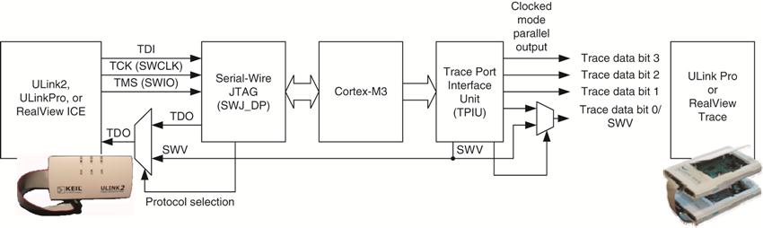
Alternatively, the SWV output mode can also share a pin with the trace output pin in clocked mode. The trace data (either in clocked mode or SWV mode) can be collected by external TPA like the ARM RealView Trace.
When instruction trace (using ETM) is required, the clocked mode is more suitable than SWV mode as it provides higher trace bandwidth. For simple data trace and event trace (e.g., tracing of exception events), the SWV mode is usually sufficient and can be used with less connection pins.
To use the TPIU, the TRCENA bit in the DEMCR must be set to 1, and the protocol (mode) selection register and trace port size control registers need to be programmed by the trace capture software.
16.6 The Flash Patch and Breakpoint Unit
The FPB has the following two functions:
• Hardware breakpoint (generates a breakpoint event to the processor to invoke debug modes such as halt or debug monitor)
• Patch instruction or literal data from Code memory space to Static Random Access Memory (SRAM) memory region
16.6.1 Breakpoint Feature
The breakpoint function is fairly easy to understand—during debugging, you can set one or multiple breakpoints to program addresses or literal constant addresses. If the program code at the breakpoint addresses get executed, or if the literal constant addresses get accessed, then this triggers the breakpoint debug event and causes the program execution to halt (for halt mode debug) or triggers the debug monitor exception (if debug monitor is used). Then, you can examine the register's content, memory contents, debug using single stepping, and so on.
16.6.2 Flash Patch Feature
The Flash Patch function allows using a small programmable memory in the system to apply patches to a program memory which cannot be modified. For products to be produced in high volume, using mask ROM or one-time-programmable ROM can reduce the cost of the product. But, if a software bug is found after the device is programmed, it could be costly to replace the devices. By integrating a small reprogrammable memory, for example, a very small Flash or Electrically Erasable Programmable Read Only Memory (EEPROM), patches can be made to the original software programmed in the device. For microcontrollers that only use Flash to store software, Flash Patch is not required as the whole Flash can be erased and reprogrammed easily.
16.6.3 Comparators
The FPB contains eight comparators:
The comparators can be used either for breakpoint function or Flash Patch function, but both do not function at the same time.
The FPB has a Flash Patch control register that contains an enable bit to enable the FPB. In addition, each comparator comes with a separate enable bit in its comparator control register. Both of the enable bits must be set to 1 for a comparator to operate.
The comparators can be programmed to remap addresses from Code space to the SRAM memory region. When this function is used, the REMAP register needs to be programmed to provide the base address of the remapped contents. The upper three bits of the REMAP register (bit[31:29]) is hardwired to b001, limiting the remap base address location to within 0x20000000 to 0x3FFFFF80, which is always within the SRAM memory region.
When the instruction address or the literal address hits the address defined by the comparator, the read access is remapped to the table pointed to by the REMAP register (see Figure 16.7).

Using the remap function, it is possible to create some “what-if” test cases in which the original instruction or a literal value is replaced by a different one; even the program code is in ROM or Flash memory. An example use is to allow execution of a program or subroutine in the SRAM region by patching program ROM in the Code region so that a branch to the test program or subroutine can take place. This makes it possible to debug a ROM-based device.
Alternatively, the six instruction address comparators can be used to generate breakpoints as well as to invoke halt mode debug or debug monitor exceptions.
16.7 The Advanced High-Performance Bus Access Port
The Advanced High-Performance Bus Access Port (AHB-AP) is a bridge between the debug interface module (Serial-Wire JTAG Debug Port or Serial-Wire Debug Port) and the Cortex-M3 memory system (see Figure 16.8). For the most basic data transfers between the debug host and the Cortex-M3 system, the following three registers in the AHB-AP are used:
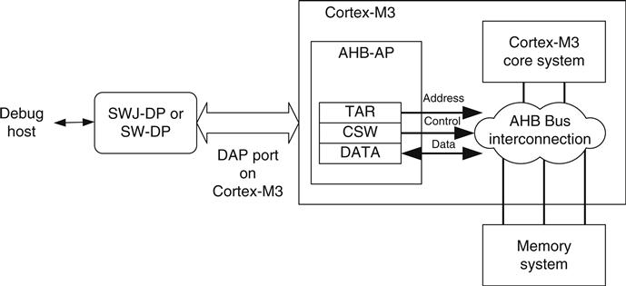
The CSW register can control the transfer direction (read/write), transfer size, transfer types, and so on. The TAR register is used to specify the transfer address, and the DRW register is used to carry out the data transfer operation (transfer starts when this register is accessed).
The data register DRW represents exactly what is shown on the bus. For half word and byte transfers, the required data will have to be manually shifted to the correct byte lane by debugger software. For example, if you want to carry out a data transfer of half word size to address 0x1002, you need to have the data on bit [31:16] of the DRW register. The AHB-AP can generate unaligned transfers, but it does not rotate the result data based on the address offset. So, the debugger software will have to either rotate the data manually or split an unaligned data access into several accesses if needed.
Other registers in the AHB-AP provide additional features. For example, the AHB-AP provides four banked registers and an automatic address increment function so that access to memory within close range or sequential transfers can be speeded up. The AHB-AP also contains a register called base address to indicate the address of ROM table.
In the CSW register, there is one bit called MasterType. This is normally set to 1 so that hardware receiving the transfer from AHB-AP knows that it is from the debugger. However, the debugger can pretend to be the core by clearing this bit. In this case, the transfer received by the device attached to the AHB system should behave as though it is accessed by the processor. This is useful for testing peripherals with FIFO that can behave differently when accessed by the debugger.
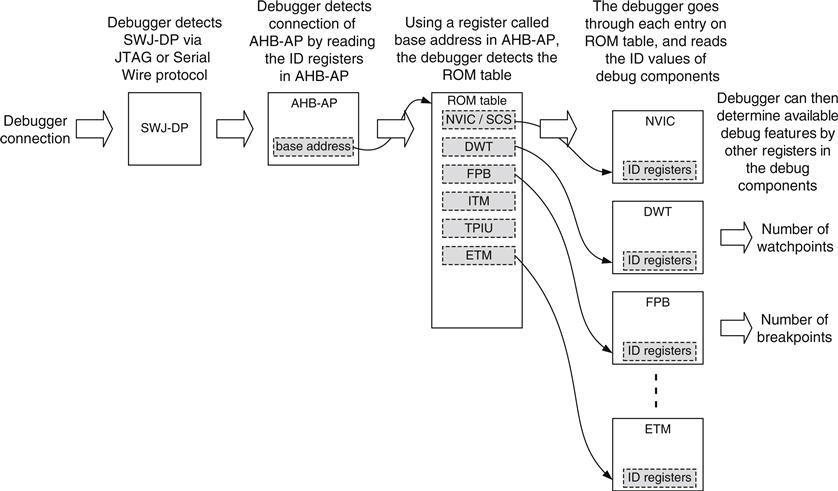
16.8 ROM Table
The ROM table is used to allow autodetection of debug components inside a Cortex-M3 chip. The Cortex-M3 processor is the first product based on ARM v7-M architecture. It has a defined memory map and includes a number of debug components. However, in newer Cortex-M devices or if the chip designers modified the default debug components, the memory map for the debug devices could be different. To allow debug tools to detect the components in the debug system, a ROM table is included; it provides information on the NVIC and debug block addresses.
The ROM table is located in address 0xE00FF000. Using contents in the ROM table, the memory locations of system and debug components can be calculated. The debug tool can then check the ID registers of the discovered components and determine what is available on the system.
For the Cortex-M3, the first entry in the ROM table (0xE00FF000) should contain the offset to the NVIC memory location. (The default value in the ROM table's first entry is 0xFFF0F003; bit[1:0] means that the device exists and there is another entry in the ROM table following. The NVIC offset can be calculated as 0xE00FF000 + 0xFFF0F000 = 0xE000E000.)
The default ROM table for the Cortex-M3 is shown in Table 16.2. However, because chip manufacturers can add, remove, or replace some of the optional debug components with other CoreSight debug components, the value you find on your Cortex-M3 device could be different.
Table 16.2
Cortex-M3 Default ROM Table Values
| Address | Value | Name | Description |
| 0xE00FF000 | 0xFFF0F003 | NVIC | Points to the NVIC base address at 0xE000E000 |
| 0xE00FF004 | 0xFFF02003 | DWT | Points to the DWT base address at 0xE0001000 |
| 0xE00FF008 | 0xFFF03003 | FPB | Points to the FPB base address at 0xE0002000 |
| 0xE00FF00C | 0xFFF01003 | ITM | Points to the ITM base address at 0xE0000000 |
| 0xE00FF010 | 0xFFF41003 | TPIU | Points to the TPIU base address at 0xE0040000 |
| / 0xFFF41002 | |||
| 0xE00FF014 | 0xFFF42003 | ETM | Points to the ETM base address at 0xE0041000 |
| / 0xFFF42002 | |||
| 0xE00FF018 | 0 | End | End-of-table marker |
| 0xE00FFFCC | 0x1 | MEMTYPE | Indicates that system memory can be accessed on this memory map |
| 0xE00FFFD0 | 0 / 0x04 | PID4 | Peripheral ID space; reserved |
| 0xE00FFFD4 | 0 / 0x00 | PID5 | Peripheral ID space; reserved |
| 0xE00FFFD8 | 0 / 0x00 | PID6 | Peripheral ID space; reserved |
| 0xE00FFFDC | 0 / 0x00 | PID7 | Peripheral ID space; reserved |
| 0xE00FFFE0 | 0 / 0xC3 | PID0 | Peripheral ID space; reserved |
| 0xE00FFFE4 | 0 / 0xB4 | PID1 | Peripheral ID space; reserved |
| 0xE00FFFE8 | 0 / 0x0B | PID2 | Peripheral ID space; reserved |
| 0xE00FFFEC | 0 / 0x00 | PID3 | Peripheral ID space; reserved |
| 0xE00FFFF0 | 0 / 0x0D | CID0 | Component ID space; reserved |
| 0xE00FFFF4 | 0 / 0x10 | CID1 | Component ID space; reserved |
| 0xE00FFFF8 | 0 / 0x05 | CID2 | Component ID space; reserved |
| 0xE00FFFFC | 0 / 0xB1 | CID3 | Component ID space; reserved |
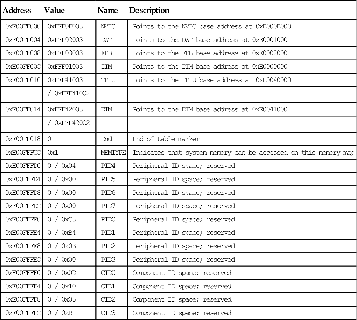
The lowest two bits of the value indicate whether the device exists. In normal cases, the NVIC, DWT, and FPB should always be there, so the last two bits are always 1. However, the TPIU and the ETM could be taken out by the chip manufacturer and might be replaced with other debugging components from the CoreSight product family.
The upper part of the value indicates the address offset from the ROM table base address. For example,
NVIC address = 0xE00FF000 + 0xFFF0F000 = 0xE000E000 (truncated to 32-bit)
For debug tool development using CoreSight technology, it is necessary to determine the address of debug components from the ROM table. Some Cortex-M3 devices might have a different setup of the debug component connection that can result in additional base addresses. By calculating the correct device address from this ROM table, the debugger can determine the base address of the provided debug component, and then from the component ID of those components the debugger can determine the type of debug components that are available (see Figure 16.9).