
The Nested Vectored Interrupt Controller and Interrupt Control
Publisher Summary
The Nested Vectored Interrupt Controller (NVIC) is an integrated part of the Cortex-M3 processor. It is closely linked to the Cortex-M3 CPU core logic. Its control registers can be accessed as memory-mapped devices. This chapter describes the basic Interrupt configuration. The NVIC supports 1–240 external interrupt inputs which are commonly known as interrupt request queues (IRQs). Procedures of setting up an interrupt have been demonstrated with examples. This chapter also throws light on the basic interrupt configurations with the help of different registers and highlights software interrupt and how it can be generated. The chapter ends with a detailed discussion on the Systick Timer which is integrated with the NVIC.
8.1 Nested Vectored Interrupt Controller Overview
As we've seen, the Nested Vectored Interrupt Controller (NVIC) is an integrated part of the Cortex™-M3 processor. It is closely linked to the Cortex-M3 CPU core logic. Its control registers are accessible as memory-mapped devices. Besides control registers and control logic for interrupt processing, the NVIC unit also contains control registers for the SYSTICK Timer, and debugging controls. In this chapter, we'll examine the control logic for interrupt processing. Memory Protection Unit and debugging control logic are discussed in later chapters.
The NVIC supports 1–240 external interrupt inputs (commonly known as interrupt request [IRQs]). The exact number of supported interrupts is determined by the chip manufacturers when they develop their Cortex-M3 chips. In addition, the NVIC also has a Nonmaskable Interrupt (NMI) input. The actual function of the NMI is also decided by the chip manufacturer. In some cases, this NMI cannot be controlled from an external source.
The NVIC can be accessed in the System Control Space (SCS) address range, which is memory location 0xE000E000. Most of the interrupt control/status registers are accessible only in privileged mode, except the Software Trigger Interrupt register (STIR), which can be set up to be accessible in user mode. The interrupt control/status register can be accessed in word, half word, or byte transfers.
In addition, a few other interrupt-masking registers are also involved in the interrupts. They are the “special registers” covered in Chapter 3 and are accessed through special registers access instructions: move special register to general-purpose register (MRS) and move to special register from general-purpose register (MSR) instructions.
8.2 The Basic Interrupt Configuration
Each external interrupt has several registers associated with it.
In addition, a number of other registers can also affect the interrupt processing:
8.2.1 Interrupt Enable and Clear Enable
The Interrupt Enable register is programmed through two addresses. To set the enable bit, you need to write to the SETENA register address; to clear the enable bit, you need to write to the CLRENA register address. In this way, enabling or disabling an interrupt will not affect other interrupt enable states. The SETENA/CLRENA registers are 32 bits wide; each bit represents one interrupt input.
As there could be more than 32 external interrupts in the Cortex-M3 processor, you might find more than one SETENA and CLRENA register—for example, SETENA0, SETENA1, and so on (see Table 8.1). Only the enable bits for interrupts that exist are implemented. So, if you have only 32 interrupt inputs, you will only have SETENA0 and CLRENA0. The SETENA and CLRENA registers can be accessed as word, half word, or byte. As the first 16 exception types are system exceptions, external Interrupt #0 has a start exception number of 16 (see Table 7.2).
8.2.2 Interrupt Set Pending and Clear Pending
If an interrupt takes place but cannot be executed immediately (for instance, if another higher-priority interrupt handler is running), it will be pended. The interrupt-pending status can be accessed through the Interrupt Set Pending (SETPEND) and Interrupt Clear Pending (CLRPEND) registers. Similarly to the enable registers, the pending status controls might contain more than one register if there are more than 32 external interrupt inputs.
The values of pending status registers can be changed by software, so you can cancel a current pended exception through the CLRPEND register, or generate software interrupts through the SETPEND register (see Table 8.2).
8.2.3 Priority Levels
Each external interrupt has an associated priority-level register, which has a maximum width of 8 bits and a minimum width of 3 bits. As described in the previous chapter, each register can be further divided into preempt priority level and subpriority level based on priority group settings. The priority-level registers can be accessed as byte, half word, or word. The number of priority-level registers depends on how many external interrupts the chip contains (see Table 8.3). The priority level configuration registers details can be found in Appendix D, Table D.19.
Table 8.1
Interrupt Set Enable Registers and Interrupt Clear Enable Registers (0xE000E100-0xE000E11C, 0xE000E180-0xE000E19C)
| Address | Name | Type | Reset Value | Description |
| 0xE000E100 | SETENA0 | R/W | 0 | Enable for external Interrupt #0–31 bit[0] for Interrupt #0 (exception #16) bit[1] for Interrupt #1 (exception #17) … bit[31] for Interrupt #31 (exception #47) Write 1 to set bit to 1; write 0 has no effect Read value indicates the current status |
| 0xE000E104 | SETENA1 | R/W | 0 | Enable for external Interrupt #32–63 Write 1 to set bit to 1; write 0 has no effect Read value indicates the current status |
| 0xE000E108 | SETENA2 | R/W | 0 | Enable for external Interrupt #64–95 Write 1 to set bit to 1; write 0 has no effect Read value indicates the current status |
| … | — | — | — | — |
| 0xE000E180 | CLRENA0 | R/W | 0 | Clear enable for external Interrupt #0–31 bit[0] for Interrupt #0 bit[1] for Interrupt #1 … bit[31] for Interrupt #31 Write 1 to clear bit to 0; write 0 has no effect Read value indicates the current enable status |
| 0xE000E184 | CLRENA1 | R/W | 0 | Clear enable for external Interrupt #32–63 Write 1 to clear bit to 0; write 0 has no effect Read value indicates the current enable status |
| 0xE000E188 | CLRENA2 | R/W | 0 | Clear enable for external Interrupt #64–95 Write 1 to clear bit to 0; write 0 has no effect Read value indicates the current enable status |
| … | — | — | — | — |
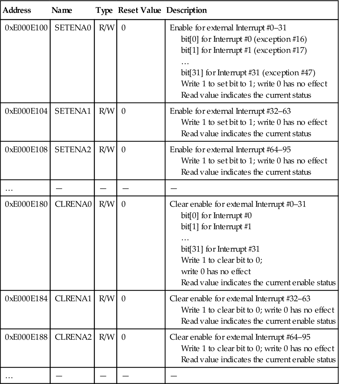
Table 8.2
Interrupt Set-Pending Registers and Interrupt Clear-Pending Registers (0xE000E200-0xE000E21C, 0xE000E280-0xE000E29C)
| Address | Name | Type | Reset Value | Description |
| 0xE000E200 | SETPEND0 | R/W | 0 | Pending for external Interrupt #0–31 bit[0] for Interrupt #0 (exception #16) bit[1] for Interrupt #1 (exception #17) … bit[31] for Interrupt #31 (exception #47) Write 1 to set bit to 1; write 0 has no effect Read value indicates the current status |
| 0xE000E204 | SETPEND1 | R/W | 0 | Pending for external Interrupt #32–63 Write 1 to set bit to 1; write 0 has no effect Read value indicates the current status |
| 0xE000E208 | SETPEND2 | R/W | 0 | Pending for external Interrupt #64–95 Write 1 to set bit to 1; write 0 has no effect Read value indicates the current status |
| … | — | — | — | — |
| 0xE000E280 | CLRPEND0 | R/W | 0 | Clear pending for external Interrupt #0–31 bit[0] for Interrupt #0 (exception #16) bit[1] for Interrupt #1 (exception #17) … bit[31] for Interrupt #31 (exception #47) Write 1 to clear bit to 0; write 0 has no effect Read value indicates the current pending status |
| 0xE000E284 | CLRPEND1 | R/W | 0 | Clear pending for external Interrupt #32–63 Write 1 to clear bit to 0; write 0 has no effect Read value indicates the current pending status |
| 0xE000E288 | CLRPEND2 | R/W | 0 | Clear pending for external Interrupt #64–95 Write 1 to clear bit to 0; write 0 has no effect Read value indicates the current pending status |
| … | — | — | — | — |

Table 8.3
Interrupt Priority-Level Registers (0xE000E400-0xE000E4EF)
| Address | Name | Type | Reset Value | Description |
| 0xE000E400 | PRI_0 | R/W | 0 (8 bit) | Priority-level external Interrupt #0 |
| 0xE000E401 | PRI_1 | R/W | 0 (8 bit) | Priority-level external Interrupt #1 |
| … | — | — | — | — |
| 0xE000E41F | PRI_31 | R/W | 0 (8 bit) | Priority-level external Interrupt #31 |
| … | — | — | — | — |

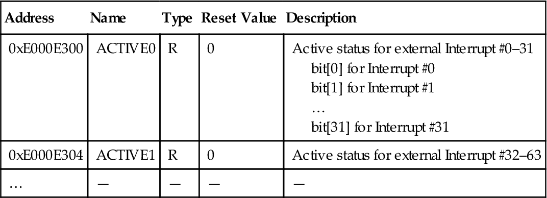
8.2.4 Active Status
Each external interrupt has an active status bit. When the processor starts the interrupt handler, the bit is set to 1 and cleared when the interrupt return is executed. However, during an Interrupt Service Routine (ISR) execution, a higher-priority interrupt might occur and cause preemption. During this period, although the processor is executing another interrupt handler, the previous interrupt is still defined as active. The active registers are 32 bit but can also be accessed using half word or byte-size transfers. If there are more than 32 external interrupts, there will be more than one active register. The active status registers for external interrupts are read-only (see Table 8.4).
Table 8.4
Interrupt Active Status Registers (0xE000E300-0xE000E31C)
| Address | Name | Type | Reset Value | Description |
| 0xE000E300 | ACTIVE0 | R | 0 | Active status for external Interrupt #0–31 bit[0] for Interrupt #0 bit[1] for Interrupt #1 … bit[31] for Interrupt #31 |
| 0xE000E304 | ACTIVE1 | R | 0 | Active status for external Interrupt #32–63 |
| … | — | — | — | — |
8.2.5 PRIMASK and FAULTMASK Special Registers
The PRIMASK register is used to disable all exceptions except NMI and hard fault. It effectively changes the current priority level to 0 (highest programmable level). In C programming, you can use the intrinsic functions provided in Cortex Microcontroller Software Interface Standard (CMSIS) compliant device driver libraries or provided in the compiler to set and clear PRIMASK:
void __enable_irq(); // Clear PRIMASK
void __disable_irq(); // Set PRIMASK
void __set_PRIMASK(uint32_t priMask); // Set PRIMASK to value
uint32_t __get_PRIMASK(void); // Read the PRIMASK value
For assembly language users, you can change the current status of PRIMASK using Change Process State (CPS) instructions:
CPSIE I ; Clear PRIMASK (Enable interrupts)
CPSID I ; Set PRIMASK (Disable interrupts)
This register is also programmable using MRS and MSR instructions. For example,
MOV R0, #1
MSR PRIMASK, R0 ; Write 1 to PRIMASK to disable all
; interrupts
and
MOV R0, #0
MSR PRIMASK, R0 ; Write 0 to PRIMASK to allow interrupts
PRIMASK is useful for temporarily disabling all interrupts for critical tasks. When PRIMASK is set, if a fault takes place, the hard fault handler will be executed.
FAULTMASK is just like PRIMASK except that it changes the effective current priority level to −1, so that even the hard fault handler is blocked. Only the NMI can be executed when FAULTMASK is set. It can be used by fault handlers to raise its priority to −1, so that they can have access to some features for hard fault exception (more information on this is provided in Chapter 12). In C programming with CMSIS compliant driver libraries, you can use the intrinsic functions provided in device driver libraries to set and clear FAULTMASK as follows:
void __set_FAULTMASK(uint32_t faultMask);
uint32_t __get_FAULTMASK(void);
For assembly language users, you can change the current status of FAULTMASK using CPS instructions as follows:
CPSIE F ; Clear FAULTMASK
CPSID F ; Set FAULTMASK
You can also access the FAULTMASK register using MRS and MSR instructions.
FAULTMASK is cleared automatically upon exiting the exception handler except return from NMI handler. Both FAULTMASK and PRIMASK registers cannot be set in the user state.
8.2.6 The BASEPRI Special Register
In some cases, you might want to disable interrupts only with priority lower than a certain level. In this case, you could use the BASEPRI register. To do this, simply write the required masking priority level to the BASEPRI register. For example, if you want to block all exceptions with priority level equal to or lower than 0x60, you can write the value to BASEPRI:
__set_BASEPRI(0x60); // Disable interrupts with priority
// 0x60-0xFF using CMSIS
Or in assembly language:
MOV R0, #0x60
MSR BASEPRI, R0 ; Disable interrupts with priority
; 0x60-0xFF
You can also read back the value of BASEPRI:
x = __get_BASEPRI(void); // Read value of BASEPRI
Or in assembly language:
MRS R0, BASEPRI
To cancel the masking, just write 0 to the BASEPRI register:
__set_BASEPRI(0x0); // Turn off BASEPRI masking
Or in assembly language:
MOV R0, #0x0
MSR BASEPRI, R0 ; Turn off BASEPRI masking
The BASEPRI register can also be accessed using the BASEPRI_MAX register name. It is actually the same register, but when you use it with this name, it will give you a conditional write operation. (As far as hardware is concerned, BASEPRI and BASEPRI_MAX are the same register, but in the assembler code they use different register name coding.) When you use BASEPRI_MAX as a register, the processor hardware automatically compares the current value and the new value and only allows the update if it is to be changed to a higher priority level; it cannot be changed to lower priority levels. For example, consider the following instruction sequence:
MOV R0, #0x60
MSR BASEPRI_MAX, R0 ; Disable interrupts with priority
; 0x60, 0x61,…, etc
MOV R0, #0xF0
MSR BASEPRI_MAX, R0 ; This write will be ignored because
; it is lower
; level than 0x60
MOV R0, #0x40
MSR BASEPRI_MAX, R0 ; This write is allowed and change the
; masking level to 0x40
To change to a lower masking level or disable the masking, the BASEPRI register name should be used. The BASEPRI/BASEPRI_MAX register cannot be set in the user state.
As with other priority-level registers, the formatting of the BASEPRI register is affected by the number of implemented priority register widths. For example, if only 3 bits are implemented for priority-level registers, BASEPRI can be programmed as 0x00, 0x20, 0x40 … 0xC0, and 0xE0.
8.2.7 Configuration Registers for Other Exceptions
Usage faults, memory management faults, and bus fault exceptions are enabled by the System Handler Control and State register (0xE000ED24). The pending status of faults and active status of most system exceptions are also available from this register (see Table 8.5).
Table 8.5
The System Handler Control and State Register (0xE000ED24)
| Bits | Name | Type | Reset Value | Description |
| 18 | USGFAULTENA | R/W | 0 | Usage fault handler enable |
| 17 | BUSFAULTENA | R/W | 0 | Bus fault handler enable |
| 16 | MEMFAULTENA | R/W | 0 | Memory management fault handler enable |
| 15 | SVCALLPENDED | R/W | 0 | SVC pended; SVC was started but was replaced by a higher-priority exception |
| 14 | BUSFAULTPENDED | R/W | 0 | Bus fault pended; bus fault handler was started but was replaced by a higher-priority exception |
| 13 | MEMFAULTPENDED | R/W | 0 | Memory management fault pended; memory management fault started but was replaced by a higher-priority exception |
| 12 | USGFAULTPENDED | R/W | 0 | Usage fault pended; usage fault started but was replaced by a higher-priority exception |
| 11 | SYSTICKACT | R/W | 0 | Read as 1 if SYSTICK exception is active |
| 10 | PENDSVACT | R/W | 0 | Read as 1 if PendSV exception is active |
| 8 | MONITORACT | R/W | 0 | Read as 1 if debug monitor exception is active |
| 7 | SVCALLACT | R/W | 0 | Read as 1 if SVC exception is active |
| 3 | USGFAULTACT | R/W | 0 | Read as 1 if usage fault exception is active |
| 1 | BUSFAULTACT | R/W | 0 | Read as 1 if bus fault exception is active |
| 0 | MEMFAULTACT | R/W | 0 | Read as 1 if memory management fault is active |
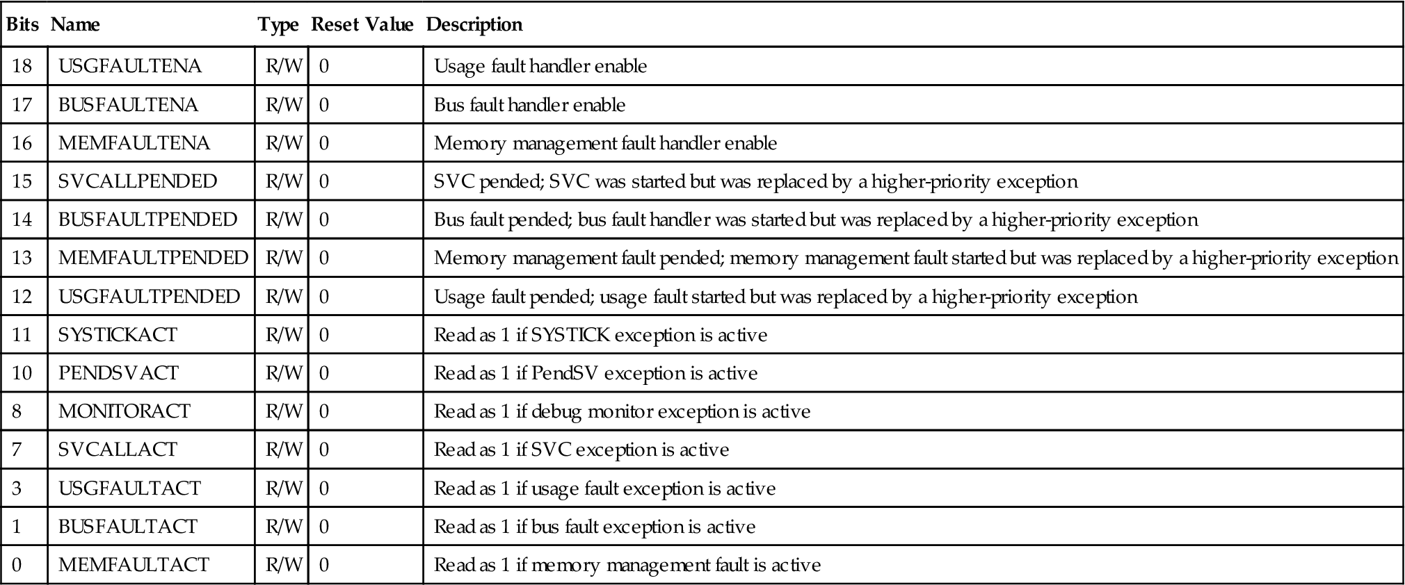
Note: Bit 12 (USGFAULTPENDED) is not available on revision 0 of Cortex-M3.
Be cautious when writing to this register; make sure that the active status bits of system exceptions are not changed accidentally. Otherwise, if an activated system exception has its active state cleared by accident, a fault exception will be generated when the system exception handler generates an exception exit.
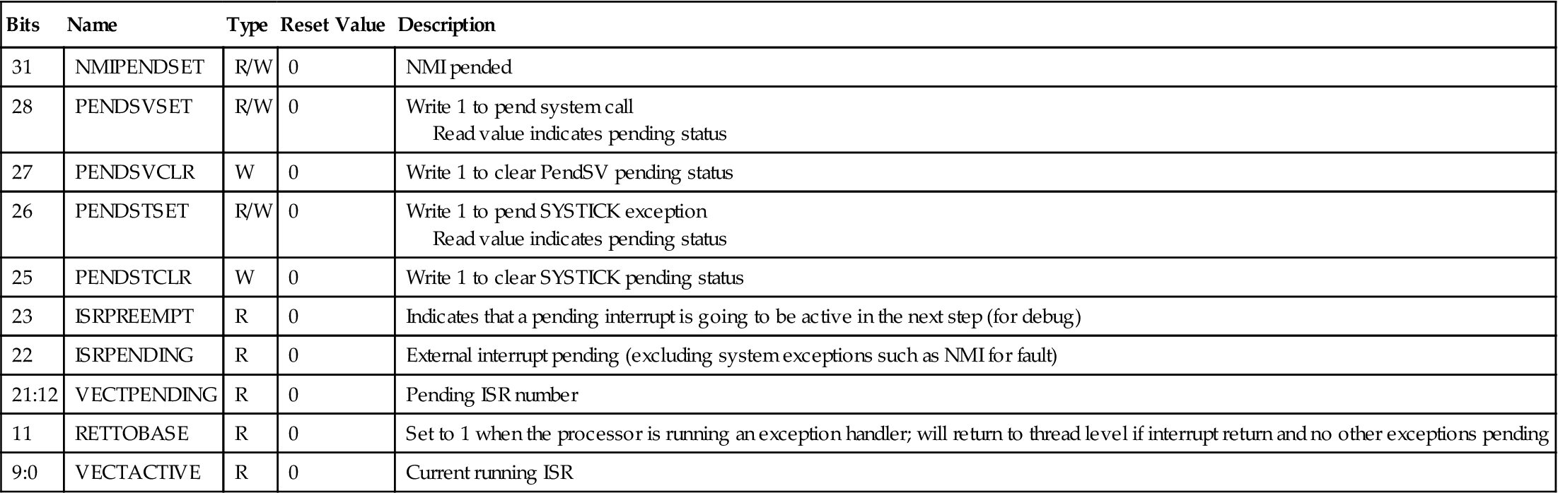
Pending for NMI, the SYSTICK Timer, and PendSV is programmable through the Interrupt Control and State register. In this register, quite a number of the bit fields are for debugging purposes. In most cases, only the pending bits would be useful for application development (see Table 8.6).
Table 8.6
Interrupt Control and State Register (0xE000ED04)
| Bits | Name | Type | Reset Value | Description |
| 31 | NMIPENDSET | R/W | 0 | NMI pended |
| 28 | PENDSVSET | R/W | 0 | Write 1 to pend system call Read value indicates pending status |
| 27 | PENDSVCLR | W | 0 | Write 1 to clear PendSV pending status |
| 26 | PENDSTSET | R/W | 0 | Write 1 to pend SYSTICK exception Read value indicates pending status |
| 25 | PENDSTCLR | W | 0 | Write 1 to clear SYSTICK pending status |
| 23 | ISRPREEMPT | R | 0 | Indicates that a pending interrupt is going to be active in the next step (for debug) |
| 22 | ISRPENDING | R | 0 | External interrupt pending (excluding system exceptions such as NMI for fault) |
| 21:12 | VECTPENDING | R | 0 | Pending ISR number |
| 11 | RETTOBASE | R | 0 | Set to 1 when the processor is running an exception handler; will return to thread level if interrupt return and no other exceptions pending |
| 9:0 | VECTACTIVE | R | 0 | Current running ISR |
8.3 Example Procedures In Setting Up an Interrupt
For most simple applications, the application is stored in ROM and there is no need to change the exception handlers, we can have the whole vector table coded in the beginning of ROM in the Code region (0x00000000). This way, the vector table offset will always be 0 and the interrupt vector is already in ROM. The only steps required to set up an interrupt will be as follows:
1. Set up the priority group setting. This step is optional. By default priority group setting is zero—only bit 0 of the priority level register is used for subpriority.
2. Set up the priority level of the interrupt. This step is optional. By default, all interrupts are at priority level 0 (highest).
Here is a simple example procedure for setting up an interrupt:
NVIC_SetPriorityGrouping(5);
NVIC_SetPriority(7, 0xC0); // Set IRQ#7 priority level to 0xC0
NVIC_EnableIRQ(7);
In addition, make sure that you have enough stack memory if you allow a large number of nested interrupt levels. Because exception handlers always use the Main Stack Pointer, the main stack memory should contain enough space for the largest number of nesting interrupts.
If the interrupt handlers need to be changed at different stage of the application, we might need to relocate the vector table to Static Random Access Memory (SRAM), so that we can modify the exception vectors. In this case, the following extra steps would be required:
1. When the system boots up, the priority group register might need to be set up. By default, the priority group 0 is used (bit[7:1] of priority level is the preemption level and bit[0] is the subpriority level).
2. Copy the hard fault, NMI handlers and other required vector to a new vector table location in SRAM.
3. Set up the Vector Table Offset register (Table 7.7) to point to the new vector table.
4. Set up the interrupt vector for the interrupt in the new vector table.
For example, this can be done in C programming with a CMSIS compliant device driver library, assume the starting address of the new vector table is defined as "NEW_VECT_TABLE":
// HW_REG is a macro to convert address value to pointer
#define HW_REG(addr) (*((volatile unsigned long *)(addr)))
#define NEW_VECT_TABLE 0x20008000 // An SRAM region for vector table
NVIC_SetPriorityGrouping(5);
…
HW_REG((NEW_VECT_TABLE +0x8)) = HW_REG(0x8); // Copy NMI vector
HW_REG((NEW_VECT_TABLE +0xC)) = HW_REG(0xC); // Copy HardFault
…
SCB->VTOR = NEW_VECT_TABLE; // Relocate vector table to SRAM
…
HW_REG(4*(7+16)) = (unsigned) IRQ7_Handler; // Setup vector
…
NVIC_SetPriority(7, 0xC0); // Set IRQ#7 priority level to 0xC0
…
NVIC_EnableIRQ(7);
The program in assembly might be something like this:
LDR R0, =0xE000ED0C ; Application Interrupt and Reset
;Control Register
LDR R1, =0x05FA0500 ; Priority Group 5 (2/6)
STR R1, [R0] ; Set Priority Group
…
MOV R4, #8 ; Vector Table in ROM
LDR R5,=(NEW_VECT_TABLE+8)
LDMIA R4!,{R0-R1} ; Read vectors address for NMI and; Hard Fault
STMIA R5!,{R0-R1} ; Copy vectors to new vector table…
LDR R0,=0xE000ED08 ; Vector Table Offset Register
LDR R1,=NEW_VECT_TABLE
STR R1,[R0] ; Set vector table to new location
…
LDR R0,=IRQ7_Handler ; Get starting address of IRQ#7 handler
LDR R1,=0xE000ED08 ; Vector Table Offset Register
LDR R1,[R1]
ADD R1, R1, #(4*(7+16)) ; Calculate IRQ#7 handler vector
; address
STR R0,[R1] ; Setup vector for IRQ#7
…
LDR R0,=0xE000E400 ; External IRQ priority base
MOV R1, #0x0
STRB R1,[R0,#7] ; Set IRQ#7 priority to 0x0
…
LDR R0,=0xE000E100 ; SETEN register
MOV R1,#(1<<7) ; IRQ#7 enable bit (value 0x1 shifted
; by 7 bits)
STR R1,[R0] ; Enable the interrupt
In cases where the software needs to be able to run on a number of hardware devices, it might be necessary to determine the following:
The Cortex-M3 has an Interrupt Controller Type register that gives the number of interrupt inputs supported, in granularities of 32 (see Table 8.7). Alternatively, you can detect the exact number of external interrupts by performing a read/write test to interrupt configuration registers such as SETEN or priority registers.
Table 8.7
Interrupt Controller Type Register (0xE000E004)
| Bits | Name | Type | Reset Value | Description |
| 4:0 | INTLINESNUM | R | — | Number of interrupt inputs in step of 32 0 = 1 to 32 1 = 33 to 64 … |

To determine the number of bits implemented for interrupt priority-level registers, you can write 0xFF to one of the priority-level registers, then read it back and see how many bits are set. The minimum number is three. In that case you should get a read-back value of 0xE0.
8.4 Software Interrupts
Software interrupts can be generated in more than one way. The first one is to use the SETPEND register; the second solution is to use the STIR, outlined in Table 8.8.
Table 8.8
Software Trigger Interrupt Register (0xE000EF00)
| Bits | Name | Type | Reset Value | Description |
| 8:0 | INTID | W | — | Writing the interrupt number sets the pending bit of the interrupt; for example, write 0 to pend external Interrupt #0 |

For example, you can generate Interrupt #3 by writing the following code in C:
NVIC->STIR = 3; /* NVIC->STIR is defined in CMSIS compliant device driver library */
This is functionally equivalent to using SETPEND register using CMSIS function:
NVIC_SetPendingIRQ(3);
System exceptions (NMI, faults, PendSV, and so on) cannot be pended using this register. By default, a user program cannot write to the NVIC; however, if it is necessary for a user program to write to this register, the bit 1 (USERSETMPEND) of the NVIC Configuration Control register (0xE000ED14) can be set to allow user access to the NVIC's STIR.
8.5 The SYSTICK Timer
The SYSTICK Timer is integrated with the NVIC and can be used to generate a SYSTICK exception (exception type #15). In many operating systems, a hardware timer is used to generate interrupts so that the OS can carry out task management—for example, to allow multiple tasks to run at different time slots and to make sure that no single task can lock up the whole system. To do that, the timer needs to be able to generate interrupts, and if possible, it should be protected from user tasks so that user applications cannot change the timer behavior.
The Cortex-M3 processor includes a simple timer. Because all Cortex-M3 chips have the same timer, porting software between different Cortex-M3 products is simplified. The timer is a 24-bit down counter. It can use the internal free running processor clock signal on the Cortex-M3 processor or an external reference clock (documented as the STCLK signal on the Cortex-M3 TRM). However, the source of the STCLK will be decided by chip designers, so the clock frequency might vary between products. You should check the chip's datasheet carefully when selecting a clock source.
The SYSTICK Timer can be used to generate interrupts. It has a dedicated exception type and exception vector. It makes porting operating systems and software easier because the process will be the same across different Cortex-M3 products.
The SYSTICK Timer is controlled by four registers, shown in Tables 8.9–8.12.
Table 8.9
SYSTICK Control and Status Register (0xE000E010)
| Bits | Name | Type | Reset Value | Description |
| 16 | COUNTFLAG | R | 0 | Read as 1 if counter reaches 0 since last time this register is read; clear to 0 automatically when read or when current counter value is cleared |
| 2 | CLKSOURCE | R/W | 0 | 0 = External reference clock (STCLK) 1 = Use processor free running clock |
| 1 | TICKINT | R/W | 0 | 1 = Enable SYSTICK interrupt generation when SYSTICK Timer reaches 0 0 = Do not generate interrupt |
| 0 | ENABLE | R/W | 0 | SYSTICK Timer enable |
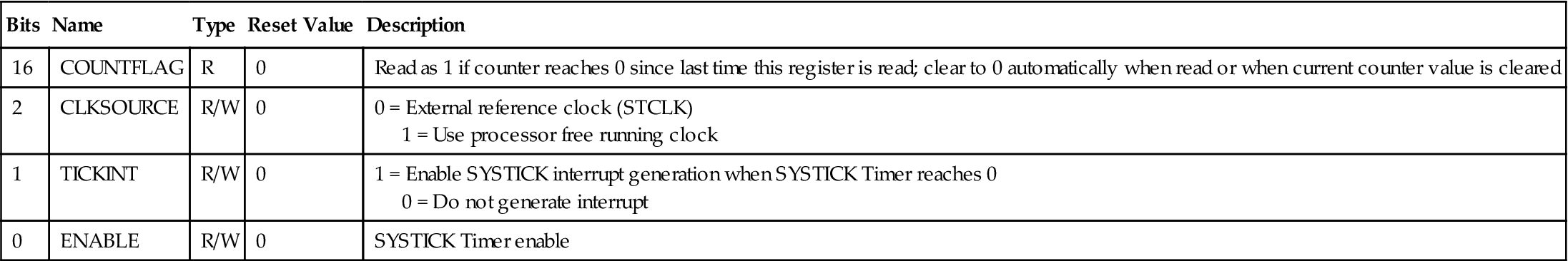
Table 8.10
SYSTICK Reload Value Register (0xE000E014)
| Bits | Name | Type | Reset Value | Description |
| 23:0 | RELOAD | R/W | 0 | Reload value when timer reaches 0 |
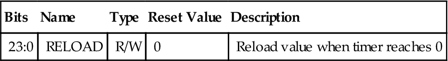
Table 8.11
SYSTICK Current Value Register (0xE000E018)
| Bits | Name | Type | Reset Value | Description |
| 23:0 | CURRENT | R/Wc | 0 | Read to return current value of the timer. Write to clear counter to 0. Clearing of current value also clears COUNTFLAG in SYSTICK Control and Status register |

Table 8.12
SYSTICK Calibration Value Register (0xE000E01C)
| Bits | Name | Type | Reset Value | Description |
| 31 | NOREF | R | — | 1 = No external reference clock (STCLK not available) 0 = External reference clock available |
| 30 | SKEW | R | — | 1 = Calibration value is not exactly 10 ms 0 = Calibration value is accurate |
| 23:0 | TENMS | R/W | 0 | Calibration value for 10 ms; chip designer should provide this value through Cortex-M3 input signals. If this value is read as 0, calibration value is not available |

The Calibration Value register provides a solution for applications to generate the same SYSTICK interrupt interval when running on various Cortex-M3 products. To use it, just write the value in TENMS to the reload value register. This will give an interrupt interval of about 10 ms. For other interrupt timing intervals, the software code will need to calculate a new suitable value from the calibration value. However, the TENMS field might not be available in all Cortex-M3 products (the calibration input signals to the Cortex-M3 might have been tied low), so check with your manufacturer's datasheets before using this feature.
Aside from being a system tick timer for operating systems, the SYSTICK Timer can be used in a number of ways: as an alarm timer, for timing measurement, and more. Note that the SYSTICK Timer stops counting when the processor is halted during debugging. Depending on the design of the microcontroller, the SysTick Timer could also be stopped when the processor enters certain type of sleep modes.
To set up the SysTick Timer, the recommended programming sequence is as follows:
• Disable SysTick by writing 0 to the SYSTICK Control and Status register.
• Write new reload value to the SYSTICK Reload Value register.
• Write to the SYSTICK Current Value register to clear the current value to 0.
• Write to the SYSTICK Control and Status register to start the SysTick timer.
This programming sequence can be used on all Cortex-M3 processors. More details of the SysTick setup is covered in Chapter 14.