
Chapter 10. Layout Parasitic Extraction and Electrical Modeling
10.1 Introduction
All electrical analysis flows are based on a methodology that incorporates a transistor or cell-based netlist with corresponding electrical parasitics from the layout interconnects annotated to the netlist to create a complete electrical model. There are layout parasitic extraction (LPE) algorithm trade-offs in terms of electrical accuracy, the number of RLC parasitic elements generated, RLC element reduction strategies (while maintaining a model of sufficient accuracy), and the EDA tool compute resources and runtime.
Traditionally, LPE tools from EDA vendors have used either of two methods for capacitance calculation, with distinct characteristics relative to these trade-offs:
A 3D field-solver algorithm—The layout cell is translated into a three-dimensional representation of interconnects and dielectrics and presented to an algorithm that solves Maxwell’s equations for an electrostatic topology. The goal is to determine the capacitance between each pair of conductors in the cell, Cij = Q/Vij. The potential difference between two wires is related to the integral of the electric field emanating from one to the other due to the electrostatic charge on the wires. In a multi-conductor model, the calculation of these electric fields from the local surface charge density on each wire results in a complex system that requires a concurrent solution for all wires. For any multi-conductor layout with strong electrostatic interactions between the conductors, an analytic solution to Maxwell’s equations is intractable. There are several numeric algorithms available to calculate an empirical solution, using either the integral or differential form of Maxwell’s equations. The two most prevalent are the boundary element method (BEM) and the floating random walk (FRW) approach.[1,2]
The BEM and FRW algorithms use an indirect technique. Assigning a reference conductor i to a potential of 1V, with all other conductors at 0V, a (numeric) solution for the total charge on each wire j provides the Cij capacitance value. Superposition theory is applied, enabling the calculation to iterate through each interconnect as a reference to complete the capacitance matrix for all wires. The BEM and FRW algorithms differ in terms of how they reach the solution for all surface charges in the layout topology; however, to achieve high extraction accuracy, either method requires substantial compute resources. As a result, 3D field-solver methods for layout parasitic extraction are commonly used only for IP library cells and smaller mixed-signal IP designs. (The FRW algorithm is much less memory intensive and extremely parallelizable, which would enable larger layout cells to be extracted, given sufficient CPU cores.)
Application of empirical formulas from representative layout topologies—The other LPE method utilizes a set of layout pattern examples, analyzed using a 3D field-solver algorithm. Capacitive formulas are then derived from the field-solver results. Dimensional parameters in the layout examples are fitted to the formula coefficients. From this set of pre-characterized layouts, the LPE tool performs a pattern match to the submitted layout cell. The specific interconnect dimensions of the layout are submitted to the formulas, which provide a capacitive value by interpolation, as depicted in Figure 10.1. Although the accuracy of the capacitance calculation is reduced by the fitted interpolation, due to the high capacity and fast throughput of the layout pattern matching approach, this method is commonly used for any large block design.
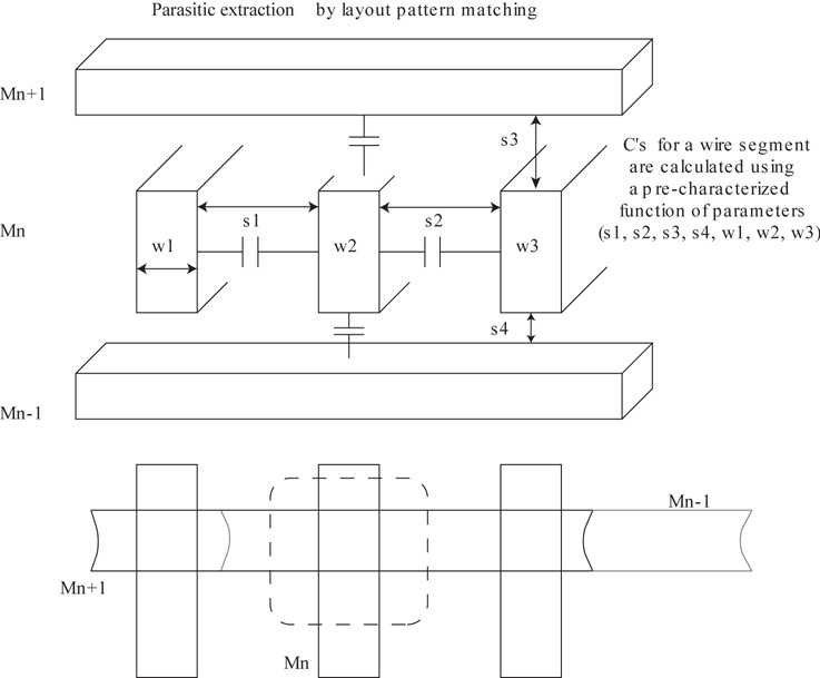
Figure 10.1 One method for parasitic extraction uses a pattern-matching method, applying a set of formulas to the specific layout pattern dimensions.
After the capacitive matrix for the layout cell is computed (using either the field-solver or pattern-matching method), the LPE tool then incorporates resistive wire segment values to provide an RC network as the parasitic netlist output.
10.1.1 Inductance Extraction
Unique LPE algorithms from EDA vendors are provided for the extraction of wire inductance, whether applied to an on-chip inductor layout cell (for the self- and mutual-inductance of wire turns), the chip pad to package pin through the top layer metal redistribution, or internal power (and clock) grids. Figure 10.2 illustrates examples of the layouts for which inductance extraction is applicable.
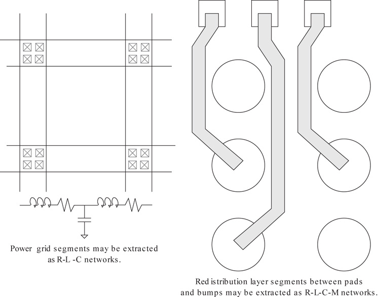
Figure 10.2 Illustration of inductance extraction, applicable to power grids, high-speed clock grids, and top-level redistribution layer connections.
These designs require accurate L and M parasitic elements for specific simulations—for example, LC-tank circuit response in analog IP, (high-speed) off-chip driver/receiver signal integrity, or on-chip power di/dt transient analysis. The balance of this chapter focuses on RC element extraction.
10.1.2 Extraction Methodology Decisions
This chapter does not delve into extraction algorithms in detail. Rather, the discussion focuses on the considerations at the points where the SoC methodology team might choose one approach over another.
The sheer volume of cells, interconnects, and available metal layers in block layouts results in very large parasitic netlists. In advanced process nodes, the layout variability is reduced (e.g., track-based routing with strict width/space design rules, FinFET device/cell placements on grid). These two characteristics suggest that the LPE flow is increasingly likely to leverage a pattern library approach for extraction, with sufficient accuracy. The parasitic extraction flow for “high-sigma” circuit characterization still requires the increased accuracy of a 3D field-solver algorithm, however.
The parasitic extraction flow involves several steps to provide the annotated netlist as output. Further, the flow is divided between circuit-level extraction for library cells (see Section 10.2) and extraction of interconnect routes (see Section 10.4).
For circuit extraction, the input layout cell is evaluated using a PDK techfile, which includes the recognition operations necessary to do the following:
Identify devices (and their width, length, and finger calculations)
Identify global supply and ground connections
Divide the layout into device versus non-device geometries
Trace valid connectivity from device nodes through contacts and metals to other circuit nodes or cell pins
Measure the layout dimensions of interest in the neighborhood of each device (for layout-dependent effects, as discussed shortly)
Note that the initial extraction steps are the same as for the layout-versus-schematic netlist verification flow—that is, identify and measure devices and then trace connections between devices. Indeed, the layout cell must be “LVS clean” to the corresponding schematic netlist for parasitic annotation to be successful (see Figure 10.3).
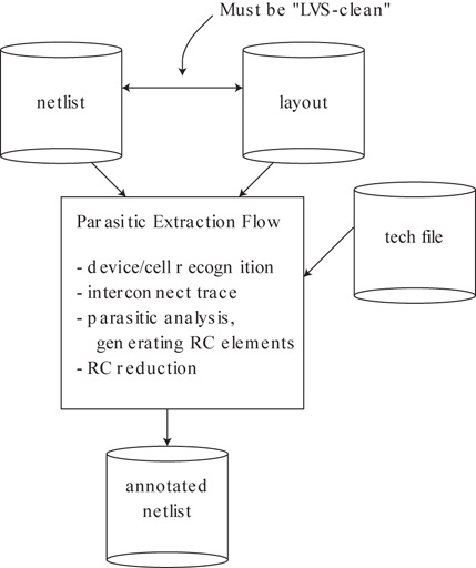
Figure 10.3 Correct annotation of LPE parasitics to the schematic netlist requires the layout to be “LVS clean.”
The layout does not need to be “DRC clean” to present to the extraction flow; annotation only requires the layout to be LVS clean. If DRC errors are present in the layout, there will be inaccuracies in the extracted resistive and capacitive elements, but annotation to a simulatable netlist would still be successful.
If the SoC design team is developing circuit-level IP, a project management decision is needed about when a layout is of sufficient quality to be presented to extraction and electrical analysis flows. If the IP layout is LVS clean but contains (minor) DRC errors, it may be prudent to submit this preliminary version layout to analysis for early identification of any major electrical issues.
10.1.3 Hierarchical Extraction of IP Macros
For circuit-level extraction of library cells, the annotation of parasitic elements is typically applied to a flat LVS netlist. For larger IP macros, an alternative approach would be to use a hierarchical model in which extraction and annotation are performed on (highly repetitive) instances within the schematic netlist presented to the LVS flow. To enable this efficiency, there must be a degree of consistency between the hierarchies for the schematic model and the physical layout view. The extraction flow would be provided with a list of correlated hierarchical LVS instance and layout view identifiers within the IP to extract/annotate once and reuse the results throughout the full model hierarchy. Wires connecting instances would be extracted separately, typically using a gray box visibility approach for the instances. The combination of hierarchical LVS and extraction is an effective method for highly regular IP macros, such as register files and arrays.
10.2 Cell- and Transistor-Level Parasitic Modeling for Cell Characterization
This section describes the extraction approaches to model custom cell layouts for analysis—specifically, the identification of the layout dimensions affecting device simulation parameters and the annotation of parasitics surrounding the devices. This section also briefly reviews the evolving nature of the characterization flow using the composite device and parasitic extraction netlist (i.e., the generation of cell electrical abstract models for release with the functional, physical, and test models as part of the IP library). The detail in these characterization models is increasing for advanced process nodes, as the EDA electrical analysis tools enhance their algorithms for increased accuracy.
10.2.1 Cell Extraction
The cell library layouts are presented to the LPE flow for extracting detailed netlists prior to characterization. This requires a “full custom” LPE techfile as input, with process cross-section and material properties. This techfile includes properties for the device fabrication layers, local metals and contacts, and substrate/well nodes.
A key consideration to review with the foundry is how parasitics are allocated to the device model and to separate extracted elements when the layout is measured. Figure 10.4 illustrates the capacitances between gate, source/drain, and substrate nodes for a planar FET device; both internal and external dimensions are associated with these capacitances. There is an added complication that the device model is likely to also include a capacitance calculation, given the area and perimeter measures of the source/drain nodes.
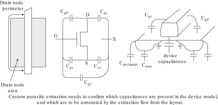
Figure 10.4 Device models may include the requisite parameters to include parasitic capacitances, in addition to the internal node-to-node capacitances, given area and perimeter measures.
Adding a local M0 interconnect layer, contacts, and metal1 wire to the layout adds to the calculation detail, as the Cgs and Cgd capacitances now include the vertical structures, as well (see Figure 10.5).
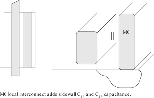
Figure 10.5 The local M0 interconnect layer adds a vertical dimension to the device parasitic capacitance extraction topologies.
The scaling of device channel length has increased the sheet resistivity of the device gate, implying that the distributed nature of the gate R*Cchannel is of greater importance, as depicted in Figure 10.6. The PDK techfile assumption for parasitic modeling of the gate also requires review with the foundry.
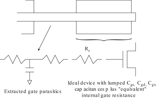
Figure 10.6 Parasitic extraction of the gate input requires review with the foundry for the definition of both the external gate parasitics and the reduced model of the distributed gate R*C.
The device-level parasitic models are significantly more complicated for FinFET devices due to both their vertical profile and the traversal of the gate between multiple fins. The allocation of internal device model versus external Cgs and Cgd extracted elements is intricate, as illustrated in Figure 10.7.
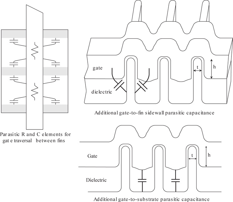
Figure 10.7 Parasitic extraction of the external parasitic capacitances for a FinFET device requires review with the foundry for the definition of the capacitances of the gate traversing between fins.
A complication is present with FinFET device models that describe a single fin and represent a multi-fin device with the schematic parameter “NFIN = n”. The extraction and annotation of Cgs, Cgd, and Rg elements to the NFIN device model requires approximation to represent the distributed capacitance and resistance of the gate traversal between the (n – 1) fins as lumped elements in the parasitic extraction netlist.
10.2.2 Layout-Dependent Effects (LDEs)
For custom extraction at the cell level, there are device behavior impacts due to layout dimensions in the neighborhood of the device. Figure 10.8 illustrates some of the measures taken during extraction. Layout-dependent effects result in adjustments to the device channel carrier mobility and threshold voltage, using additional input parameters on the device model.
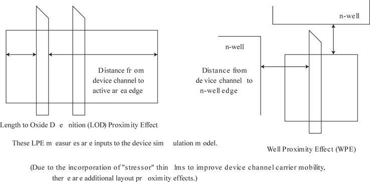
Figure 10.8 Illustration of several layout-dependent effect measurements required for custom layout parasitic extraction. These measurements are inputs to the device model.
The LVS techfile commands incorporate additional measurements for the LDE effects. The device simulation model is enhanced to apply these parameter measurements to adjust the carrier mobility and threshold voltage. Note that the LDE measurements differ for individual device fingers, which are connected in parallel to implement a wide device. As a result, although the input schematic draws the multi-fingered device using a single symbol, the LVS output netlist expands fingers into individual device instances, with specific layout-dependent effect measures for each.
The foundry may include the impact of a new layout-dependent effect measured on fabricated devices during the bring-up of a new process, using an application programming interface (API) software layer added to the existing device model, as depicted in Figure 10.9; this allows circuit characterization to proceed prior to the release of an updated compact model standard.[3]
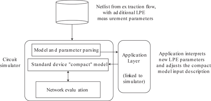
Figure 10.9 To enable new layout dependent effects not reflected in the standard device model, an API software layer may be added. The new LDE measures are reflected in a new output netlist generated by the parasitic extraction flow. The API simulation layer then modifies the existing device model accordingly.
The layout-dependent effects apply to device extraction, not the calculation of parasitic R and C elements for device netlist annotation. As a result, the foundry PDK defines how these effects are represented. The measurement of layout-dependent effects involves a key methodology decision. When library cells are being extracted, a cell needs to be surrounded by a representative layout environment so that devices at the cell edges receive suitable proximity measures, as illustrated in Figure 10.10.
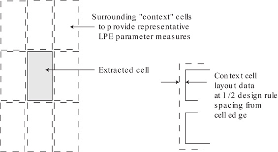
Figure 10.10 Context cells surround the layout cell being extracted to provide representative proximity measures for perimeter devices.
The choice of the cell surround (and route overlay) data used for parasitic extraction, and thus for subsequent cell characterization, is a subjective methodology decision. The ultimate goal is to provide accurate cell pin delay arcs, consistent with the path timing margins used in the static timing analysis flow.
As an aside, the emergence of layout-dependent effects has changed the nature of library cell design engineering project planning. Traditionally, IP design engineers would capture their schematic design and define the individual device dimensions, specify the number of device fingers, and (potentially) enter layout estimates for the device node area and perimeter. This schematic representation was sufficient to submit directly to a circuit simulator. Once the optimal schematic dimensions were achieved for the PPA targets for the IP cell, the schematic was reviewed with the layout engineer for physical implementation. The engineering review might include a discussion of any specific layout assumptions made during the schematic-based simulation phase. With the introduction of layout-dependent effects, it is much more difficult to develop a suitable schematic-only model for design simulations; a representative (and iteratively refined) cell layout is required to extract the proximity measurements. The circuit and layout design engineers collaborate much more closely, with cell layout activity commencing much earlier in the library development schedule. The traditional “throw the schematic over the wall to the layout engineer” methodology is no longer adequate. In addition, there is increasing interest in the productivity benefits of automated generation of cell IP layouts (as briefly mentioned in the “Future Research” section in Chapter 9). An initial cell layout generated “semi-automatically” could provide a sufficiently accurate extracted model to capture important LDE characteristics and then be iteratively refined by the design and layout engineering team.
10.2.3 Extraction Corners
Each PVT characterization corner reflects a specific combination of process fabrication variations, applied voltage at the device (including supply voltage and ground distribution I*R drop margins), and device temperature to be used in subsequent electrical analysis flows. The set of process fabrication variations includes both device parameters and wire measures. The device variations are typically represented by a single set of model parameters that result in an n-sigma device current at the voltage and temperature values for the corner (see Figure 10.11).
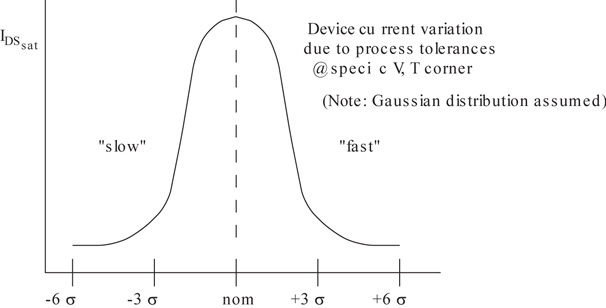
Figure 10.11 The device model parameters selected for characterization at a particular corner represent a composite n-sigma device current. For library cells, this is typically n = 3.
The extracted elements for wires introduce unique corners, adding to the number of characterization simulations. These wire extraction settings reflect the interdependence between wire thickness, resistance, and coupling capacitance. The foundry provides PDK support for the wiring extraction corners, including the following:
Max_Ctotal (R will be low) and min_Ctotal (R will be high)
Max_RC (Ccoupling low, R*Cground high)
Min_RC (Ccoupling high, R*Cground low)
Nominal_RC
For multipatterned metal layers, the overlay tolerance for a decomposed mask layer introduces spacing variations between adjacent wires. This additional source of variation introduces new MP variants for existing corners. Again, the foundry assesses which of the many potential extraction settings sufficiently cover the variation space and provides the PDK techfile support. EDA tool vendors have optimized their extraction algorithms such that derivation of parasitic netlists for multiple corners requires a minor increase in runtime.
The SoC methodology team evaluates which extraction corners to annotate to the device netlist for the electrical analysis flows—timing, power, and noise.
Note that the EDA industry has proposed an extracted netlist format that would include multiple value entries for each R and C element that would represent a statistical range rather than a single element value. To date, however, this representation has not displaced the use of separate netlists for each corner.
10.2.4 Introduction to Cell Characterization
The extracted netlist of devices (and related layout-dependent effect parameters) with the annotated parasitic elements is presented to the cell characterization flow, which initiates a number of circuit simulations with specific input/output conditions and measurement criteria. From these measured data, a number of electrical models are derived (e.g., delay arc models, input gate load and output drive strength impedance, noise propagation from each input pin to output, cell power dissipation). The level of detail in these models has evolved substantially with process node scaling to provide greater accuracy. Correspondingly, the EDA tool algorithms have evolved to leverage this additional detail. For example, in early VLSI processes, gate delay was much larger than interconnect delay; a lumped capacitive load, rather than a Ceff load and distributed RC interconnect network, was sufficient for delay calculation. These early delay arc models used a simple linear equation for the dependency on output capacitive load and input signal slew.
This linear model was increasingly inaccurate for submicron process nodes. The non-linear delay dependency evolved to a representation using the set of measured values from characterization simulations entered into two-dimensional tables. The Non-Linear Delay Model (NLDM) tables provided the arc delay and output pin slew as a function of capacitive load and input slew, as before (see Figure 10.12).
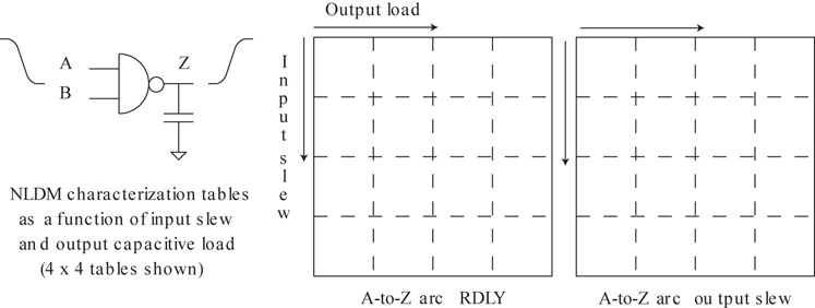
Figure 10.12 Illustration of arc delay characterization data as a set of Non-Linear Delay Model (NLDM) tables, with output capacitive load and input signal slew as the independent variables.
Concurrently, the effective capacitive load Ceff and separate RC interconnect network delay methodology was introduced, as described in Section 9.1. The (NxM) dimensionality of the NLDM tables for characterization of each delay arc was selected to adequately cover the Cload and input slew ranges while limiting the (N*M) simulations required to populate the data in the tables for characterization throughput. More recently, the NLDM approach has been augmented by a more general methodology that records the output waveform in detail for each of the N*M simulations rather than using a single slew-based signal transition value.[4] Figure 10.13 illustrates one of the general modeling approaches in use to represent the output. The result of cell characterization is a non-linear output driver current source that is to be connected to the distributed RC load network.
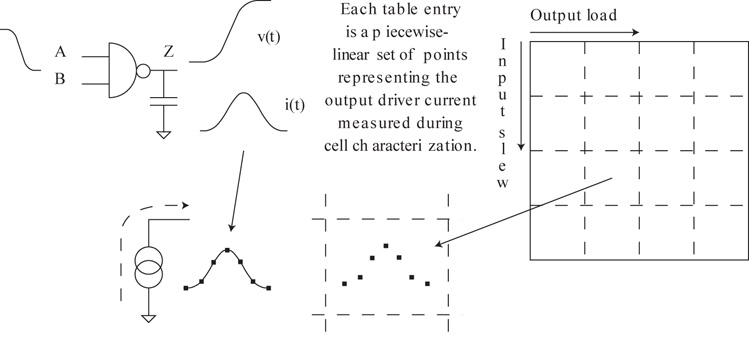
Figure 10.13 An alternative to the single NLDM output signal slew uses a set of (value, time) data for each table entry, representing a non-linear current (or voltage) source. A new set of characterization flow measurements is required.
The waveform detail is stored using a set of time points, so the non-linear source model is actually piecewise linear. The characterization slew table no longer uses fixed NLDM value entries but rather a set of (time, value) pairs from sampling the simulation measures.
This enhanced library cell format also includes a feature to describe specific side-input pin values in the case where the measured input-to-output pin response is a strong function of the (static) values on other inputs, as shown in Figure 10.14. This state-dependent delay model requires significantly more characterization simulations.
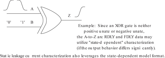
Figure 10.14 An extension to the library cell characterization model includes support for multiple tables, based on specific (static) values at other cell inputs.
The cell’s input pin capacitance model has also recently been expanded. Rather than a fixed Cgate for the input pin devices, multiple values can be used to represent the voltage-dependent device and Miller input capacitance behavior.
With these general representations, a different delay calculation and propagation algorithm approach is used by the related EDA analysis tools. Specifically, interconnect delay and noise propagation algorithms need to solve an interconnect network model with the (piecewise-linear) driver, fan-out receiver capacitances, and extracted RC parasitic elements. The remainder of this section uses both the NLDM and general current/voltage source driver model approaches in the description of cell characterization methods.
Note that the temperature value used in characterization simulations affects both the device model and the extracted resistive elements in the RC network. The resistor model in the foundry PDK includes temperature coefficients (TC1 and TC2):
10.2.5 Characterization Ranges and Corner Values
The IP library provider defines the range of load capacitance and input pin slew rates over which characterization values are measured for each corner. The SoC methodology team has several engineering decisions to make after reviewing the characterization settings.
Algorithm for Out-of-Range Delay Calculation
During the delay calculation phase of static timing analysis, a specific cell instance may have an effective load capacitance or input pin arrival slew outside the characterization range. The calculation algorithm would typically attempt to extrapolate from the delay table entries. The SoC team may choose to simply accept the calculation or may request that an error be reported by the tool such that a design modification can be made. As illustrated in Figure 10.15, a large input slew or large output load implies a significant transient cross-over current and cell power dissipation, as well as delay inaccuracies associated with the extrapolation.
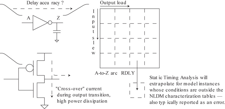
Figure 10.15 Delay calculation requiring extrapolation from the characterization table ranges is typically reported by the timing flow, due to the high internal cell cross-over current and delay accuracy error.
Algorithm for Voltage Values Differing from the Characterization Corner
Modern SoC designs may include multiple IP voltage domains and/or dynamic voltage frequency scaling (DVFS) “boost/throttle” modes, where a voltage regulator adjusts the domain supply. Alternatively, the supply voltage regulation tolerances from nominal for the specific SoC end product application may differ from the characterization assumptions. As a result, the operating environment may include voltages that differ from the IP characterization values. Traditionally, CMOS circuit delays were adequately described as a linear function of supply voltage; for example, if characterization used a (VDDnom– 10%) assumption at the cell for slow timing, but the product application could ensure (VDDnom – 5%) was provided, a performance boost of ~5% could be assumed. However, with newer process nodes, this assumption is less accurate. The active device input overdrive of |VDD —Vt| as a percentage of VDD is smaller because VDD has been scaled faster than the device threshold. As device dimensions have scaled, VDD has been reduced to adhere to electric field limits for reliability; conversely, to maintain suitable circuit noise rejection, Vt has not been reduced correspondingly.
To support unique operating voltage conditions, the SoC methodology team needs to assess whether a single delay multiplier will be sufficiently accurate or whether additional characterization corners at specific voltage(s) are required, with project cost and schedule impact.
10.2.6 Multiple-Input Switching (MIS)
A fundamental cell characterization assumption for pin-to-pin delay arcs is that other input pins are at static values. However, if other inputs are also switching in a narrow time window around the pin transition, the measured cell delay and output slew may differ significantly, as depicted in Figure 10.16.
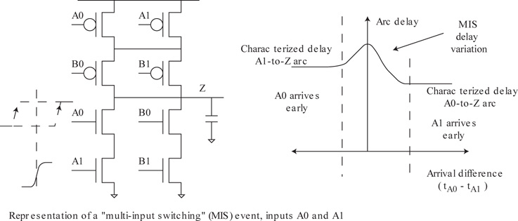
Figure 10.16 Illustration of a multiple-input switching (MIS) event and the potential delay calculation inaccuracy associated with characterization using static side inputs (also refer to Figure 4.18).
There is no well-defined methodology for incorporating multiple-input switching (MIS) events into characterization libraries. An ad hoc approach would be to examine the critical paths reported by static timing analysis and explore the input signal arrival times on the non-critical delay arcs. If another arrival time might impact the critical delay, an additional timing margin may be warranted. There have been proposals to enhance statistical static timing analysis algorithms to better support MIS. Probabilistic input pin arrival times reflect cell and extracted interconnect variation. A convolution of multiple arrival time distributions during timing analysis would provide a single input distribution to use with a (statistical) gate delay model to generate an output timing distribution.[5,6,7,8]
10.2.7 Logically Symmetric Inputs
Figure 10.16 illustrates the impact of an MIS event on the cell delay arc. In the figure, the single input switching delay arc values differ for the two logically symmetric logic gate input pins. The library data model for each cell indicates the sets of inputs that are logically equivalent. A common physical synthesis and physical implementation timing optimization is to evaluate a swap of the nets connected to equivalent pins to move a timing-critical input arrival to a faster delay arc.
10.2.8 Sequential Circuit Characterization
In addition to the clock-to-output delay arc, the delay characterization of a flip-flop cell includes the measurement of the data-to-clock setup time and the clock-to-data hold time tables. The measurement criteria used during characterization by the IP provider should be reviewed by the SoC methodology team to evaluate against the delay margin assumptions used in timing analysis. Specifically, the definition of flip-flop setup time (and hold time) is typically based on the allowed increase in clock-to-output delay, as the data transition occurs closer to the clock edge, as illustrated in Figure 10.17.
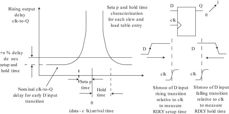
Figure 10.17 Flip-flop setup time in cell characterization is typically defined using a clk-to-Q delay pushout criterion, measured using a simulation sweep of clock-to-data arrival transitions.
A shmoo of circuit simulations at each corner sweeps the data transition toward the clock edge, and the clock-to-output delay for the new data value is measured to establish the setup time; that is, the setup time equates to an n% increase in clock-to-output delay from the delay of a stable data input. Similarly, a sweep of a data transition back to the clock edge is performed, and the clock-to-output delay for the trailing data value is measured to establish the hold time.
The SoC methodology team needs to be aware of this characterization measurement. An engineering judgment may be needed to review failing paths from the timing analysis flow (especially if the project is approaching the tapeout target schedule). Referring again to Figure 10.17, there will be an increase in clock-to-output delay for data input arrivals failing the setup time. However, if the setup timing test fails by a small interval and the timing slack for the flop’s clock-to-output path launch is positive by a sufficient margin, the arriving path setup test fail could potentially be waived. Any timing waiver would need to be granted judiciously; the clock-to-output delay curve in Figure 10.17 is very steep for data transitions not far from the selected setup time.
10.2.9 Input Pin Noise Characterization
A capacitive-coupled transient from aggressor nets to a victim net propagates to the input pins of fan-out cells. The fan-out cells suppress a (small) input transient, with a reduced perturbation on the output. As a result, the noise pulse presented to the next level fan-out is diminished; an example is depicted in Figure 10.18. This filtering applies to the complementary transistors of CMOS logic circuits. Other logic types are much more sensitive to input pin noise, such as precharged domino circuits or inputs to data-steering transfer gates. The circuit characterization for input noise limits involves a low-up and high-down input pin noise transient. (For completeness, a high-up and low-down transient is also being characterized: The increased electric field magnitude/duration across the device gate-to-channel for these transients would introduce a reliability concern.)
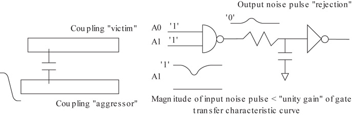
Figure 10.18 A cell input pin noise transient is propagated to the cell output.
The pin noise characterization strategy has evolved over process node scaling as the aspect ratio of metal lines has changed and the relative contribution of coupling capacitance has increased. The most direct method would be to compare the magnitude of the input noise pulse to the DC transfer characteristic of the cell. As long as the input pin noise is well below the high-gain transition slope of the (Vout, Vin) curve, the output fully suppresses the input perturbation (see Figure 10.19).
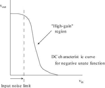
Figure 10.19 Noise model using the (Vout versus Vin) DC transfer characteristic curve. Suppression occurs for an input noise pulse magnitude below the high-gain region of the curve.
Cell characterization simply generates the transfer curve and selects a single noise magnitude limit. This approach is extremely conservative and does not scale well to the impact of increased coupling. Of specific consideration is that both the magnitude and duration of the input noise transient influence the output behavior (for a given load capacitance). A higher-magnitude pulse may be acceptable if the duration is limited. This behavior led to the definition of an input noise immunity curve (NIC), as illustrated in Figure 10.20.
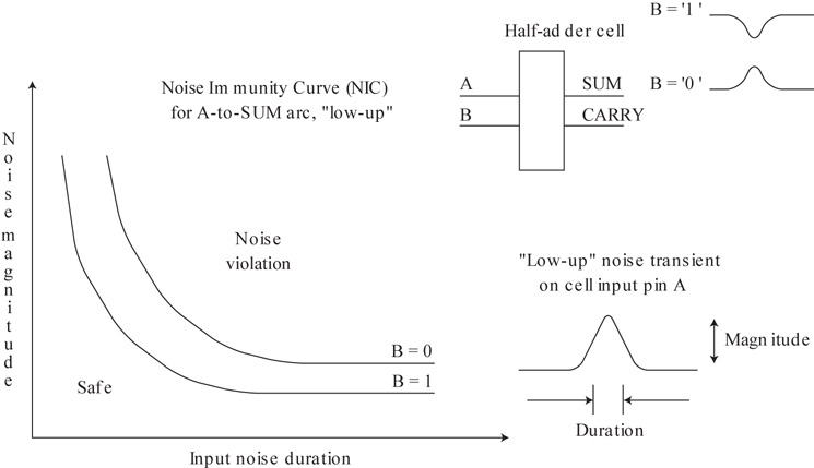
Figure 10.20 An enhanced noise model utilizes a noise immunity curve (NIC) developed during cell characterization.
The characterization assumption is that the typical input pin noise perturbation on-chip is adequately modeled as a (smoothed) triangular ramp. The noise immunity curves in Figure 10.20 define the edge between the acceptable (“safe”) and violating output response when the cell instance is being evaluated during the noise analysis flow. The figure depicts immunity curves for an arc with different static values assigned to side inputs. The IP provider is faced with the decision of how many NIC models to generate for each arc, with a commensurate increase in the number of characterization simulations. The typical approach is to release only a single NIC for each arc and use the results for the side input values providing highest sensitivity to the input pin noise event.
The subsequent noise analysis flow, like static timing analysis, would commonly be exercised without functional vectors, leading to the use of a single, conservative NIC for each arc. (The noise analysis flow would accept functional and timing exclusions to reduce the superposition of potential aggressor noise sources, as described in Section 12.2.)
The key requirement for noise analysis is whether signal transients propagate to a flop input, such that an error state value could be recorded. Rather than apply a check at each cell input pin during the noise analysis flow using the DC transfer characteristic or the NIC curve, a more general approach is to calculate the output response to an input noise event and initiate analysis of the next stage in the path, as depicted in Figure 10.21.
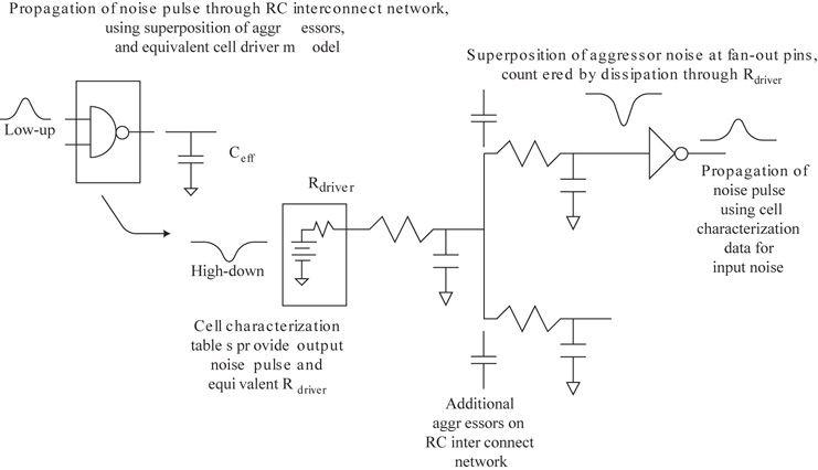
Figure 10.21 Illustration of noise propagation to subsequent stages in a path to a flip-flop input.
Propagation involves analysis of a (linear) network, consisting of a driver voltage source and resistance model, the RC interconnects, additional aggressor sources, and the receiver capacitance. As with the general time-based output transition waveform recorded during characterization described earlier in this section, cell characterization for noise would measure and store a set of output waveform data from cell input pin noise transients. An illustration of the noise characterization propagation arc for a high-down input pulse is depicted in Figure 10.22.
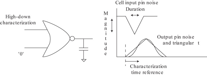
Figure 10.22 Example of a noise propagation arc model from cell characterization.
The output pulse data would reflect the magnitude and delay of the response to the input transient; either detailed (voltage, time) points or a fitted triangular output pulse could be recorded. The characterization input pulse set should span a wide range of magnitude, duration, and Cload values. The intent of the general analysis algorithm is to allow greater propagated noise in the network toward a flop test endpoint rather than the more restrictive individual cell limits.
This discussion of the impact of coupling noise transients has focused on the behavior of quiescent victim nets. There is also a corresponding impact on the delay of a pin-to-pin arc if the injected noise occurs during a transition on the victim net, as illustrated in Figure 10.23.
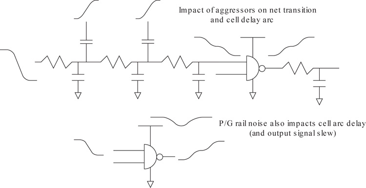
Figure 10.23 A noise transient from aggressors to a victim net in transition impacts the arrival time at the victim fan-outs. A similar noise-delay impact arises due to voltage transients on the power and ground rails.
The presence of dynamic voltage transients on the local supply/ground rails also contributes to additional noise on the driving waveform. As a result, the traditional definition of a single input signal slew used in cell characterization does not accurately represent a noisy signal at the fan-out cell inputs. Various technical approaches have been developed to calculate an “effective slew” for the noisy input to use with existing characterization data and a cell delay adder based on the (approximate) derivative of the waveform at points in the signal transition.[9,10]
10.2.10 Cell Power Characterization
To support power optimization in the synthesis and physical implementation flows, a cell power model is released as part of the IP library. Characterization of this model at each corner includes both static sub-threshold leakage power and dynamic power during a switching event. The dynamic measure describes the internal power dissipation during the output transition, separate from the energy dissipated in charging/discharging the fan-out capacitive load. The magnitude of the internal power for a single-stage logic cell is related to the crossover current and thus is a strong function of the input slew and output load capacitance. The internal power is commonly represented by a table with slew and load as the input parameters, similar to the NLDM delay arc table.
As with the other electrical characterization models, the internal and leakage power dissipation for a pin-to-pin arc is dependent on the static values assigned to other cell pins. Again, the IP provider needs to assess whether the additional characterization simulations are warranted in order to provide a full state-specific pin power model. (As mentioned below, optimization flows would not have detailed simulation data that would use a state-based pin power model.)
The SoC methodology team needs to review the library power characterization data to confirm that values are provided for the following:
Vectorless static leakage—For synthesis.
Vectorless internal power dissipation, used with an output switching activity factor measurement—Provided to the synthesis and physical design flows.
Internal power dissipation for input pin-to-output pin arcs—Used with functional simulation vectors from selected validation testcases for detailed peak/average power calculation by the power analysis flow; stateless or full state-specific pin power models could be applied.
The vectorless characterization values are appropriate for the algorithms that require fast calculations for cell selection optimization.
10.3 Decoupling Capacitance Calculation for Power Grid Analysis
Analysis of the voltage drop on the power and ground distribution grids is required to ensure that the cell voltage margin assumptions used during characterization are not exceeded. It is common to assume either a percentage of the supply or a fixed voltage drop as the local VDD and GND values present at the cell for characterization simulations, as shown in Figure 10.24.
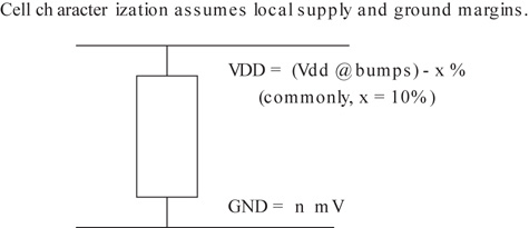
Figure 10.24 Cell characterization uses a power and ground voltage margin for circuit simulation.
The power grid voltage drop analysis can proceed using either of the following:
A conservative DC static I*R drop calculation with active “on” devices drawing their saturated current—As depicted in Figure 10.25, the placed cells are represented by current sources connected to the power and ground distribution. The current source values are equivalent to the (maximum) saturated current of the pullup and pulldown devices in the cell. The static solution assumes that all cells on the rail would be active simultaneously. The extracted model for the power and ground rails reflects the resistance of the metals, vias, and contacts in the power and ground grids.
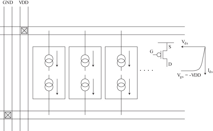
Figure 10.25 A static DC power rail voltage drop analysis would inject (saturated) device currents from each cell, with the (conservative) assumption that all cells are active concurrently.
A dynamic I*R voltage drop analysis, using current pulses injected on the rails—Functional simulation testcases exercised on the cell-based netlist are used to identify the detailed switching activity. Static timing analysis flow results provide useful information for each cell, including the following:
Output pin driver current waveform for each delay arc for the specific Cload and input slew in the static timing analysis model
The cell RDLY and FLDY delay values for each arc
The earliest and latest arrival times for each input pin for each corner
To realize the improved accuracy of dynamic I*R analysis, the extracted power/ground model needs to include both resistive and capacitive elements. The response of the local power and ground voltages to the current from multiple cells switching on a rail relies on the decoupling capacitance in close proximity to the cells. The extraction and annotation algorithms for the power/ground nets need to include the layout recognition definitions and electrical models for both internal parasitic capacitance and explicitly added decoupling capacitance, as illustrated in Figure 10.26.
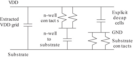
Figure 10.26 Illustration of explicit and implicit parasitic capacitances to include with the extracted rail model for dynamic I*R analysis.
10.4 Interconnect Extraction
Section 10.1 describes the metal and via cross-section stack definition for the SoC and the related conductor and inter-level dielectric material properties used by the extraction algorithm. This section expands briefly on that introduction and discusses additional properties of the extracted R and C elements for the interconnect wires between cells. The most efficient method for interconnect extraction uses a library of patterns for which parameterized R and C values have been calculated. The distributed capacitance is allocated to interconnect network nodes established for the metal wire during fracturing, such that the sum of the discrete C elements equals the total capacitance. Resistive elements are based on the (fractured) metal segment path.
When evaluating signal interconnects, the extraction flow needs to apply a method to represent the IP layout data under the route. Specifically, the two approaches used are denoted as black box and gray box extraction, as illustrated in Figure 10.27.
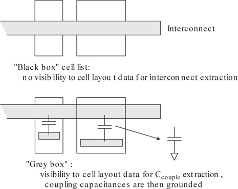
Figure 10.27 Illustration of gray box and black box IP layout data for interconnect parasitic extraction.
If a black box cell list is provided to the interconnect extraction flow, no layout data within the cell is visible to extraction. This approach is the most efficient, which is a major consideration when extracting over a number of PVT corners. Conversely, gray box extraction exposes the detailed cell layout data with the routed interconnects. Additional coupling capacitances are generated between the route and the shapes within the cell. As there are no nodes in the route netlist for these internal cell locations, the extracted capacitive elements would be lumped to ground (coupling factor, k = 1) for parasitic annotation. The gray box method is more compute intensive, and many of the additional capacitive elements are small; however, it provides a more complete model. The SoC methodology and CAD teams need to evaluate the accuracy versus compute resource trade-offs when preparing the black box and gray box cell lists for the interconnect extraction flow.
10.4.1 Resistivity
The previous section highlights the fact that the resistive elements extracted for IP library cell layouts include temperature coefficients of resistivity in their models (e.g., for Rgate, Rdrain, Rsource, R_M0, R_M1). Similarly, the metal layers used for interconnects include TC1 and TC2 coefficients in the models provided by the foundry. The interconnect metal layers may also include a width-dependent sheet resistance calculation (see Figure 10.28).
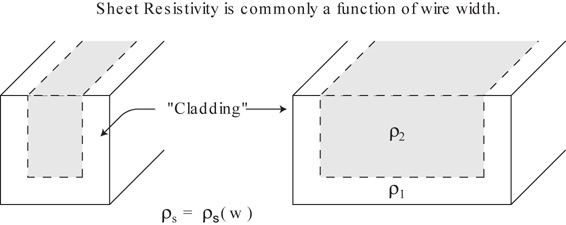
Figure 10.28 The foundry model for parasitic interconnect extraction may include a sheet resistivity value that is a function of the route width.
The fabrication of interconnects typically involves the deposition of an initial metal “cladding” layer in the damascene trench, followed by the subsequent (predominantly Cu) metal deposition. The (fixed) thickness cladding has a different material resistivity than Cu, resulting in a sheet resistivity that is a function of the linewidth. Vias result in a resistance added to the extracted netlist, based on the interconnect overlap area. The calculation of the via (or contact) resistance is more complex if the resistivity of one of the interconnect layers is significantly higher than the other; the calculation requires identification of the current through the via/contact at the leading edge of the high-resistivity material.
10.4.2 Coupling Capacitances and “Multipliers”
Figure 10.1 illustrates some of the geometric topologies that contribute to the extracted capacitances for interconnect wires. The fracturing of the layout separates the different topologies based on adjacent wire spacing and wires present above and below. The parasitic netlist output from the extraction flow consolidates the coupling capacitances between signals to avoid double-counting. However, a key SoC methodology decision is needed when submitting the annotated netlist to subsequent electrical analysis flows. When a net is analyzed, the effective coupling capacitances could be significantly different from the values determined by the geometry, as shown in Figure 10.29. A k-factor coupling multiplier is used by the analysis flows to represent the different aggressor and victim signal transitions in the figure to scale the extracted coupling capacitances in the RC interconnect model.
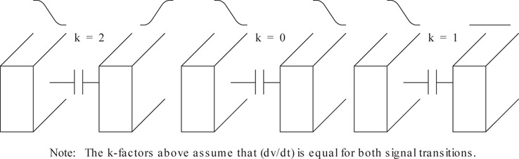
Figure 10.29 The parasitic extraction coupling capacitances between interconnects are typically subjected to a k-factor multiplier in analysis flows to reflect the “effective” coupling capacitance.
10.4.3 Parasitic Netlist Reduction
Layout fracturing for extraction can result in a very large number of R and C elements in the final network. (In the most detailed parasitic network output format from EDA extraction tools, layout coordinates are included with the R and C elements for reference, as an informational comment.) Several electrical analysis flows do not need this level of detail; a reduced netlist that provides a comparable electrical response for the signal’s spectral frequency range of interest would be sufficient and would result in significantly improved flow runtime.
The SoC methodology team needs to establish the appropriate reduction settings in the extraction flow, such as:
Equivalent R and C values for arrayed vias (see Figure 10.30)
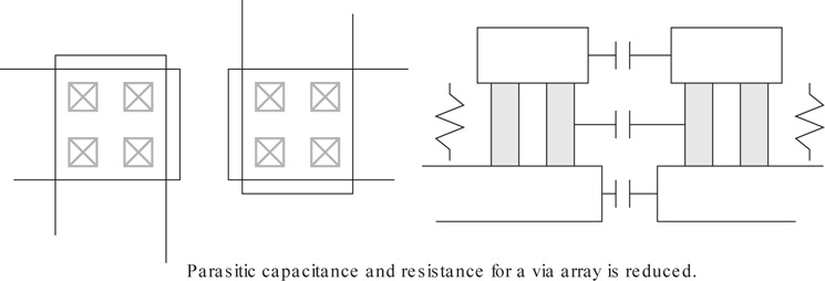
Figure 10.30 The resistive and capacitive parasitic values of a via array are typically reduced to single R and C elements.
Magnitude of coupling capacitances that can be lumped to ground
A large number of coupling capacitances stresses the runtime of reduction algorithms, and converting small Cc elements to grounded caps is a common network transformation, as shown in Figure 10.31.
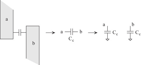
Figure 10.31 Parasitic coupling capacitance elements below a threshold are commonly converted to grounded capacitances at the node during network reduction.
Reduced RC networks are typically suitable for signal net timing analysis, noise analysis, and power rail voltage drop analysis. However, electromigration (EM) analysis relies on a detailed calculation of the current density through all interconnects, vias, and rails. The non-reduced extracted netlist is submitted to the EM analysis flow.
10.5 “Selected Net” Extraction Options
Layout parasitic extraction tools from EDA vendors incorporate multiple methods that tradeoff runtime versus (non-statistical) model accuracy. The most detailed method adopts a 3D field-solver algorithm, as described in Section 10.1. However, this approach is far too compute intensive to use for all interconnect nets; the faster, albeit less accurate, pattern-matching algorithm is used instead. The EDA extraction tools offer a feature to request field solver–level accuracy on a small set of selected nets.
10.5.1 Clock Arrival Analysis
A unique methodology flow is commonly developed for the analysis of clock nets at each extraction corner:
Extract all interconnect branches of the clock repowering tree signals using the field-solver option.
Annotate the RC elements of the clock tree to the block/chip netlist (without reduction).
Excise the cell and RC instances for the full clock tree from the total netlist.
Submit the excised netlist to circuit simulation, measuring the arrivals at the clock tree endpoints.
Compare the measured arrivals against the skew targets to assess the success of the physical implementation clock-balancing steps.
For static timing analysis, override the delay calculation for clock buffers and assign the measured arrival from circuit simulation at the clock tree endpoints to the STA model prior to evaluating the setup and hold tests.
The clock tree circuit simulation testcases also provide current measures through the (non-reduced) parasitic R elements for electromigration analysis.
The justification for this additional flow complexity (i.e., replacing buffer cell and interconnect delay calculation with detailed circuit simulation for clocks) depends on the SoC clock frequency specification and skew targets. Excising the full clock model for simulation requires handling the extracted coupling capacitances to the clock nets. Commonly, the coupling capacitances are multiplied by a k-factor = 2 or a k-factor = 0, depending on the specific clock delay skews to be amplified. For very-high-frequency clocks, the physical implementation flows commonly include features to shield clock wires to the maximum extent possible to reduce the number and magnitude of coupling capacitances to be excised from the netlist for circuit simulation.
10.6 RLC Modeling
As mentioned briefly in Section 10.1, EDA vendors offer unique tools to extract (self- and mutual) inductance of interconnects. The common applications for extracting a parasitic network of R, C, L, and (potentially) M elements are:
Models for the thick top metal redistribution layer (RDL) patterns from chip bumps to power/ground grids
Models for the RDL between chip bumps and I/O pads associated with high-speed interface drivers/receivers
Models for (very-high-frequency) clock grids
The power grid RLC models are typically merged with corresponding package models and then exercised using dynamic power current transients. Although local current transients rely on decoupling capacitance to minimize supply/ground bounce, the overall chip plus package RLC model must also be analyzed for global voltage fluctuations. The analysis of a full end-to-end driver-to-receiver model of a high-speed (SerDes or parallel DDR) interface requires circuit simulation-level detail and full RLC parasitics. The design of advanced microprocessors and SoCs pushing multi-gigahertz frequencies requires RLC modeling of the global clock grids.[11] The principal difficulty in accurate extraction of interconnect inductance is the identification of the “return current loop.” The CAD team and EDA vendor need to review how the loop will be identified through the metal stack and die well/substrate.
10.7 Summary
This chapter briefly reviewed the extraction of parasitic elements for annotation to a netlist model for use in electrical analysis flows. For cell-level IP, extraction identifies the schematic devices in the cell layout and determines the parasitic R and C elements to connect to the devices. At advanced process nodes, device-level identification includes proximity measures associated with layout-dependent effects. The merged device and RC parasitic netlist for the cell-level design is submitted to a (large) number of characterization simulations to generate the timing, noise, and power models for the library IP release.
For block-level and global-level interconnect routes between cells, extrac-tion generates a large number of parasitic RC elements. The methodology team needs to review the extraction algorithms used for capacitive coupling calculation and RC parasitic reduction prior to netlist annotation, to assess the resulting accuracy of interconnect delay calculation and to establish suitable margins in electrical analysis flows.
The extraction of inductive parasitic elements is increasing in applicability, for detailed electrical analysis of the chip-package power delivery network and for full transmit-to-receiver model simulation of high-speed chip I/O interfaces.
An increasing complication to any extraction methodology is the determination of the PVT corners at which extraction algorithms are to be evaluated, corresponding to the corners at which electrical analysis flows will be exercised. The methodology team needs to evaluate the trade-offs between analysis across a wide range of PVT variation and the resources/runtime required to run the flows and interpret the results.
EDA vendors are continuing to make a significant investment in extraction technology. Specifically, there is a requirement to apply field solver-based extraction algorithms to a greater set of IP designs seeking to apply models of the highest accuracy in electrical analysis flows. There is little value in pursuing high-sigma statistical simulation of device models if the accuracy of the extracted interconnects annotated to the devices is lacking. EDA vendors are focused on providing large model custom extraction with high parasitic accuracy and manageable compute resource.
References
[1] Kao, W., et al., “Parasitic Extraction: Current State of the Art and Future Trends,– Proceedings of the IEEE, Volume 89, Issue 5, May 2001, pp. 729–739.
[2] Iverson, R.B., and Le Coz, Y.L., “A Stochastic Algorithm for High Speed Capacitance Extraction in Integrated Circuits,” Solid-State Electronics, Volume 35, Issue 7, July 1992, pp. 1005–1012.
[3] Compact device simulation models (for numerous fabrication technologies) are reviewed and approved by the Compact Model Coalition, a group within the Si2 Consortium: https://projects.si2.org/cmc_index.php. This compact model standard approach allows EDA vendors to qualify their circuit simulation tools against these models prior to customer release. The prevalent source for many compact model proposals is the Device Group at University of California-Berkeley: https://www-device.eecs.berkeley.edu/research.htm.
[4] Trihy, R., “Addressing Library Creation Challenges from Recent Liberty Extensions,” IEEE 45th Design Automation Conference (DAC), 2008, Paper 26.5, pp. 474–479.
[5] Salzmann, J., Sill, F., and Timmermann, D., “Algorithm for Fast Statistical Timing Analysis,”2007 International Symposium on System-on-Chip, 2007, pp. 1–4.
[6] Liou, J.J., Cheng, K.T., Kundu, S., and Krstic, A., “Fast Statistical Timing Analysis by Probabilistic Event Propagation,– IEEE 38th Design Automation Conference (DAC), 2001, pp. 661–666.
[7] Devgan, A., and Kashyap, C., “Block-Based Static Timing Analysis with Uncertainty,” IEEE International Conference on Computer-Aided Design (ICCAD), 2003, pp. 607–614.
[8] Agarwal, A., Dartu, F., and Blaauw, D., “Statistical Gate Delay Model Considering Multiple Input Switching,” IEEE 41st Design Automation Conference (DAC), 2004, pp. 658–663.
[9] Nazarian, S., et al., “Modeling and Propagation of Noisy Waveforms in Static Timing Analysis,” Proceedings of the Design, Automation, and Test in Europe (DATE) Conference, 2005, pp. 776–777.
[10] Hashimoto, M., Yamada, Y., and Onodera, H. “Equivalent Waveform Propagation for Static Timing Analysis,– IEEE Transactions on Computer- Aided Design of Integrated Circuits and Systems, Volume 23, Issue 4, 2004, pp. 498–508.
[11] Deutsch, A., et al., “On-Chip Wiring Design Challenges for Gigahertz Operation,” Proceedings of the IEEE, Volume 89, Issue 4, 2001, pp. 529–555.
[12] Murrmann, H., and Widmann, D., “Current Crowding on Metal Contacts to Planar Devices,– IEEE Transactions on Electron Devices, Volume ED-16, Issue 12, December 1969, pp. 1022–1024.
Further Research
Via/Contact Resistance
Describe the requirements for via/contact resistance modeling when the two layers connected are of significantly different resistivity (and, thus, the current density in the via/contact is non-uniform). Specifically, describe the definition of current crowding and its role in resistance calculation.[12]
BEM and FRW Extraction Methods (Advanced)
The BEM and FRW methods for high-accuracy extraction differ significantly in the 3D model formulation and solution calculation.
Describe the model capacity, compute resource, runtime, and accuracy trade-offs associated with these methods (including the opportunity for algorithm parallelization).