
8
Advanced Characterization and Techniques
Raja Murugesan
JSS College of Pharmacy, Department of Pharmaceutics, No:20, Rocklands, Ooty, Tamilnadu, 643001, India
8.1 Introduction
The emergent significance of two‐dimensional (2D) nanomaterials are determined by the continuous innovation of new properties such as optical, electrical, and mechanical, which further strengthen their utility toward electronic [1, 2], energy storage [3], and biomedical domain [4]. The graphene is one of the most 2D nanomaterials due to their physicochemical properties and high energetic capability [5, 6], and also, transition metal dichalcogenides (s) having good fundamental properties involve practical applications [5]. The specific determination of the properties of the nanomaterials is the most important section in nanotechnology and which can be executed by advanced techniques that are responsive to nanoscale dimensions (nm) [7]. In recent years, nanomaterials' advanced characterization techniques involve determination of character of nanosized materials. In this content, the main objective of this chapter is to describe the main advanced techniques existing, which can be used in the characterization of nanomaterials (morphology), in terms of structure and physicochemical properties. The functionalized nanomaterials are involved in various applications such as health, food products, and biomedical application (drug delivery, gene delivery). Figure 8.1 shows the characterization techniques of nanomaterials associated with various fields such as health, biomedical, food, etc.
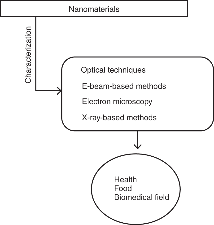
Figure 8.1 Schematic diagram of characterization involved nanomaterials.
8.2 Characterization Techniques
8.2.1 Optical Techniques – Dynamic Light Scattering (DLS)
Optical techniques are developing the beam of light scatter to acquire the analytical information on nanomaterials, whereas generally, energy is transfer from photons to the species of interest as discussed in more detail later. Moreover, elastic scattering also plays a major role. Dynamic light scattering (DLS) is one of the important methods for characterizing nanoparticles for particle size distribution regularly in “colloidal solution” [8]. Numerically appropriate the auto‐correlation method communicates to the time‐dependent fluctuations of the light scattered obtained from their Brownian motion to the particle speed. For this reason, it's depending on the particle size including their distribution of particle size. Moreover, the ISO certified that DLS techniques give good sensitive and reproducible methods. As well as DLS does not allow distinguishing between particles and aggregates [9].
If the molecule size is smaller than the frequency of light conceded through the colloid, then it is called Raleigh scattering. In Raleigh scattering, the power of dissipated radiation is uniform in all directions. When the molecule size is bigger than the wavelength, it is known as an elastic scattering of light or Mie dispersing scattering and it is mainly involved in the rotational and translational degrees of the individual particle [10, 11]. The intensity of light scattered depends on individual particle and dependent angle; in this strategy, the equation is shown below:
where
- Io is the intensity
- Λ is the wavelength
- r is the distance of scattering center
- θ is the angle
- n is the refractive index (RI)
- d is the diameter size of the particle.
At the point when mono‐chromatic light rays involve in colloidal particles, especially suspension or dilute solution, the light is dispersed with an alternate recurrence which is identified with the size of the nanoparticles. Also, they provided the RI value of solvent and solute. In this strategy, these scattering rays acquired from macromolecule obstruct fluctuations are made constructively or destructively. Therefore, the intensity of scattered light is either varying on the detection plane or scattering [10, 12]. Moreover, the Brownian motion of the particles also involves the fluctuation of scattering light intensity. DLS determined this intensity fluctuation by “Doppler's effect”; for this effect, intensity of scattered radiation level was somewhat different from the incident radiation. Also, DLS involves the autocorrelation capacity of Stokes–Einstein or the photon autocorrelation function. If the individual particle is affecting the source, then the intensity of scattered radiation was higher than incident radiation and vice versa (VV), and the frequency distribution level was broader than incident radiation. These frequency detected process was very difficult but can be able detected by “autocorrelation techniques” via time domain. The intensities of scattered light t and t + ד are formed in new positions like I(t) and I(t + ד) due to diffusion particles. If ד is near to zero, then the values of I(t) and I(t + ד) are also the same. If suppose time (t) increases, the intensity was decreased. The fundamental supposition of DLS is that the nanoparticles suspended in a liquid are moving in the Brownian movement, which is otherwise called the “Random walk” of the nanoparticles. This development is an aftereffect of the irregular impacts of the particles with the dissolvable atoms that cause the particles to diffuse through the medium. In this strategy, autocorrelation is described by exponential decay function, which is associated with the D (diffusion function) and K (measurement vector). Then, the translational diffusion/hydrodynamic diameter was calculated by using Stoke's equation. Figure 8.2 shows a schematic representative of DLS instrumentation. The equation is shown below:
where
- Rh is the hydrodynamic radius of the particle
- K is Boltzmann constant
- T is the temperature in Kelvin
- n is viscosity medium
- D is the translational diffusion coefficient
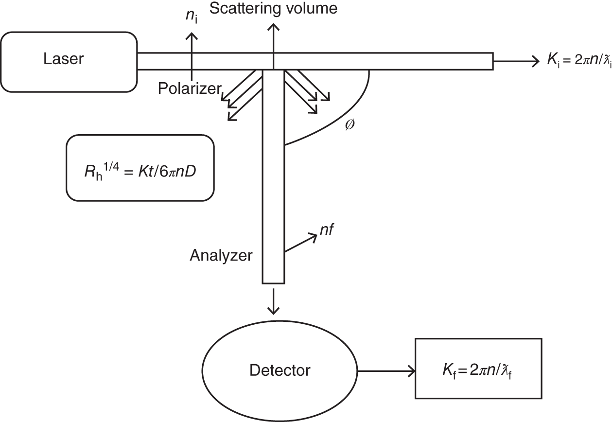
Figure 8.2 Schematic diagram of DLC techniques.
The particle diameter determined by using the abovementioned equation hard‐sphere shows the same translational diffusion coefficient of the particles. However, spherical particles do not interact with themselves. Also, the correlator involved in DLS experimental function can be able to generate an “Autocorrelation function.” Moreover, DLS experimental function can be able to determine polydispersity (PDI) sample by using Gaussian distribution. The following equation is:
where
σ is the standard deviation
The value of D (translational diffusion coefficient medium) depends on the particle movement of the medium. So, the determination of diameter obtained by DLS depends not only on size but also on shape, structure, and solvent, level of concentration, and various types of electrolytes (medium). If any change occurs from the surface area of the particle, it may affect the diffusion speed and obvious size of the particle [13].
8.2.2 Optical Spectroscopy
Optical spectroscopy is one of the most important techniques for differences reflection and transmittance already proven for 2D nanomaterials. The utilization of optical microscopy‐based portrayal methods has been firmly bound to the conceived and development of the field of 2D materials [14–18]. These methods are broadly used because they are easily implemented and also non‐destructive. These techniques are generally having a powerful tool for analyzing different types of 2D nanomaterials such as SiO2/Si [19, 20] and TMDCs (dichalcogenides) [21].
In the ultra violet–visible (150–800 nm) and near (800–2500 nm)/mid (2.5–20 mm) infrared area of the electromagnetic range, photons also instigate the electron transition modes such as vibration or rotational. UV–visible spectroscopy probes the electronic structure of a material and gives quantitative data utilizing the Beer–Lambert law, that is, the proportionality of the grouping of the analyte to the absorbance signal. Specifically compelling for nanomaterials techniques are surface plasmon resonances (SPRs), which reflect aggregate motions of electrons in the UV–visible system at metal nanoparticles in colloidal solution. Therefore, nanoparticles' size, shape, RI, and aggregation level were derived [22]. For example: metal nanoparticles such as Ag, Au, and Cu and carbon‐based materials such as carbon nanotubes (CNTs), graphene, etc.
8.2.3 NMR‐Nuclear Magnetic Resonance Spectroscopy
Nuclear magnetic resonance (NMR) spectroscopy is very useful to utilize radio wave range (wavelengths). Wave range is one of the most quantitative analytical methods for determining the structural information of nanomaterials.
The magnetic field involves the interaction of radio waves with nuclei that contain odd quantities of neutrons or protons that show evidence of the intrinsic magnetic moment, which can be able to possess resonant condition or flipping condition of spin state. Moreover, the resonant condition mainly depends upon the nuclei, chemical bonds, and functional groups. In addition, organic and inorganic compounds in both forms such as solid and liquid can be determined and also used for the synthesis of novel compounds and determination of chemical structures of biomolecules and polymers [23, 24].
8.2.4 Infrared Spectroscopy (IR) and Raman Spectroscopy
Infrared spectroscopy (IR) and Raman spectroscopy are the non‐destructive techniques; it provides electronics and structural information of nanomaterials with high spatial resolution [14] and high spectra (vibrational and rotational). IR spectroscopy directly involving in vibrational and rotational transitions ranges between 4000 and 400 cm; this range facilitates the permanent change of dipole moment. Conversely, Raman spectroscopy depends on the photons (inelastic scattering) at the electron mist of the particle requiring an adjustment in polarizability, which brings about a Raman shift and vibrational/rotational excitation. Subsequently, IR and Raman gave correlative molecular data, as regularly IR‐inactive modes are Raman‐active modes and VV. With regard to nanomaterials characterization, Fourier transform infrared (FT‐IR) spectroscopy is basically used to examine the surface modification such as “ligand attachment” of nanomaterials. Specifically, organic molecules involved in characteristic adsorption of IR spectra due to the “fingerprint region” range from 10 to 25 mm. Henceforth, these types of organic nanomaterials are involved in the drug delivery system, e.g. nanoliposomes, and also used to the modification of nanoparticles with proteins [25]. Moreover, IR spectra involve in situ measurement for matrix molecules like water. Water is a highly strong IR absorber. In this strategy, these types of interfaces possess to minimize the usage of specific probing methods such as infrared attenuated total reflection infrared spectroscopy () provided surface sensitivity and a signal limited to the diffusion depth of the transitory field [26]. Integrally, Raman spectroscopy depends on scattering processes with the small fraction of the occurrence of photons prompting vibrational modes through inelastic processes able to make stoke lines (e.g. less energy of emitted photons compared with incident photons) and anti‐stoke (e.g. high energy of emitted photons compared with incident photons). Furthermore, Raman spectra having only one primary photon range from 106 to 107, the remaining signal scales are an incident photon, and lasers are required to the light source.
Raman spectroscopy is one of the most standard characterization methods of carbon‐based nanomaterials such as graphene and graphite; the characteristic bands are located at the 1580 cm−1 and the 2D band at 2700 cm−1. A third attribute, the D band, around 1350 cm−1 is not Raman spectra, its defects of the pristine graphene band value. The D band also called as “defect induced band.” The G band at 1586 cm−1 results from in‐plane vibration sp2 carbon atoms and is the majority significant feature of graphite materials. The 2D band involved in double resonance (e.g. second‐order overtone) process indicates scattering of two photons with the opposite moment with K point of symmetry (stacking order) due to the “Brillouin zone of graphene.” Raman spectroscopy is also used in the investigation of CNTs, metal oxides, nano‐belts, quantum dots, and nanorods [27]. However, in certain metal nanoparticles, they may additionally improve the Raman signals known as surface‐enhanced Raman spectroscopy (), which is used in the determination of plasmonic and chemical enhancement effects signal ranging from 108 to 1011, which is able to characterize such nanomaterials in innovative details [28].
8.2.5 X‐Ray Photoelectron Spectroscopy (XPS)
X‐ray photoelectron spectroscopy (XPS) techniques are one of the most quantitative and qualitative determinations of the surface of the nanomaterials. XPS spectrum represents the number of distinguished electrons as an element of the binding energy inside a material when it is bare to an X‐ray beam. It is called as “Photoelectric effect.” The composition of elements can be identified within materials because each material has its characteristic peak binding energy. These peaks of individual elements are very sensitive for the electron configuration process due to their location and shape. In this strategy, it is extremely viable to investigate the electron state, chemical composition, and bonding of atoms of the nanomaterials. XPS is generally a high‐sensitive method, so it can able to analyze the nanomaterials surface within 10 nm. Moreover, it is used to the quantitative determination of the chemical composition of within materials [29] and few XPS quantitative material measurements obtained accurate as ±10% and can be expressed as:
where
- Ii is the intensity of photoelectron peak (p) for the element (i)
- Ni is the average atomic concentration of element (i) in the surface under analysis
- σi is photoelectron cross‐section for the element (i) expressed by peak (p) or Scofield factor
- ƛi is the inelastic mean free path of a photoelectron from element (i) expressed by peak (p).
- K is other factor related to the quantitative detection of a signal
Figure 8.3 The XPS analytical methods depends on the kinetic energy and binding energy expressed as
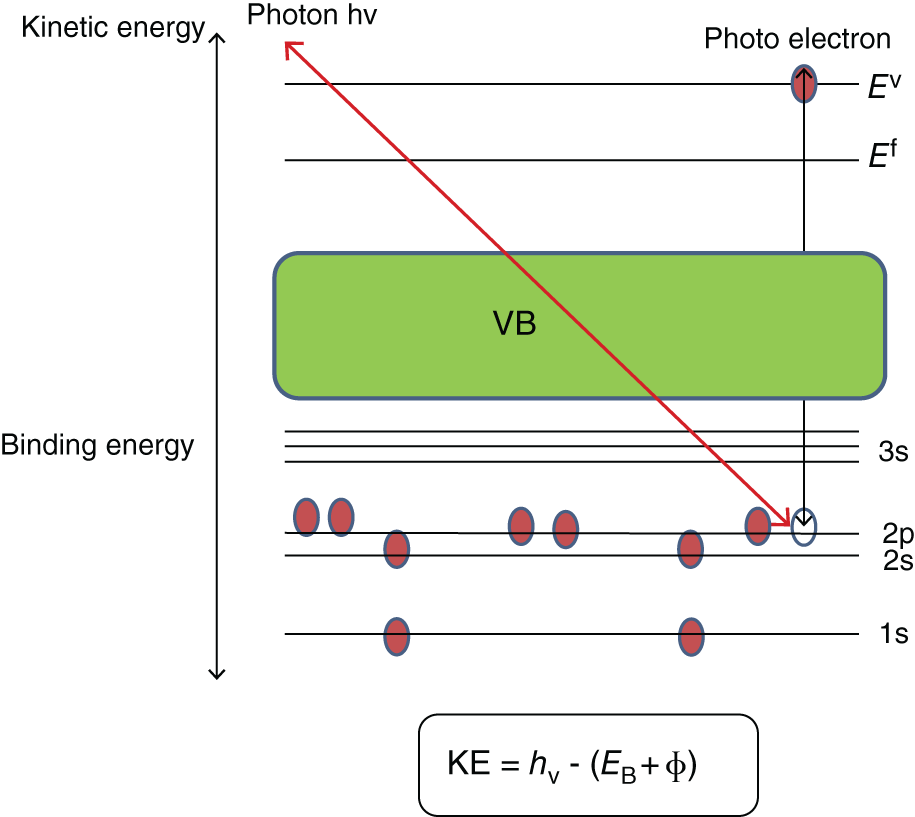
Figure 8.3 Schematic diagram of XPS techniques.
8.2.6 Characterization Based on Interactions with Electrons or Electron Microscopy (EM)
When an electron beam is used to illumine the specimen to generate a magnified image, it is known as electron microscopy (EM). Various types of EM techniques are as follows:
- Scanning electron microscopy (SEM)
- Transmission electron microscopy (TEM)
- Scanning transmission electron microscopy (STEM)
- Scanning tunneling microscopy (STM)
8.2.6.1 Scanning Electron Microscopy (SEM)
SEM is especially constructive to visualize nanomaterials. Most of the conventional microscopy is used in glass lenses for magnifying image but EM is used in the electrons. SEM produces highly magnified, three‐dimensional (3D) image. Also, this is impossible for light microscopy. When an electron ray with an increase of velocity of (3–30 keV) is engaged in the sample, the actuated auxiliary and backscattered electrons are utilized for imaging. Because of inelastic scattering, secondary electrons (s) with low‐level energy were generated. Also, SE produces signal to escape depth from the surface. Moreover, SEM is generally manufactured with advanced electron optics and field emission (FE). In this strategy, which make to avoid the chromatic and spherical aberration nature of nanomaterials in the resolution of the nanometer (nm).
Utilizing low‐voltage SEM improves the surface affectability, decreases harm of the imaged nanomaterials, and essentially decreases the depth level of electron penetration in spatial resolution ranging from 0.4 to 1.6 nm. Furthermore, low‐voltage high‐resolution SEM is used for the determination of morphology, size, and structure of 2D nanomaterials such as metallic, semi‐metallic, and inorganic compounds. Besides, non‐conductive materials such as C or Pt are also applied (Figure 8.4).

Figure 8.4 SEM technique.
This type of microscopy works under vacuum. Therefore, samples have to prepare very carefully specific procedures. Biological samples are needed for drying and shriveling. The sample is supposed to conductive of the electricity, while passing electricity was illuminated by an electron beam. Generally, a sputter coater was coated with a thin layer of “gold” (Au). So, this coating has affected the properties of the sample. The scanning vacuum was fashioned with columns, followed by a beam of a high level of energy electrons generated by “electron gun.” These beam movements to downwards for the purpose of focusing sample spot during magnetic lenses. Also, the beam focused on back and forth transversely specimen row by row throughout the set of scanning coils.
SEs are banging loose from the surface of the major sample in being there high electron beam hits the sample. These SEs are detected by an appropriate detector and augmented. A last instructive, these emitted electrons used to make for an innovative composite image. In this strategy, this type of image gives a depth of external morphology, chemical composition, texture, and structure of nanomaterials, while these images produced different types of variations such as 2D and spatial variations. Furthermore, scanning mode can be able to make images in the 5 μ to 1 cm breadth of the sample. Besides, SEM had a good capacity of magnifying images ranging from 20X to 30 000X and spatial resolution ranging from 50 to 100 nm.
SEM is frequently combined with the energy‐dispersive X‐ray spectroscopy (EDX) method, which is involved in the determination of element present, the composition of elemental at various positions. SEM–EDX is the most useful characterization methods for nanomaterials such as metallic compositions e.g. Gold, Silver, Cobalt Chloride, and palladium [30]
The field emission scanning electron microscopy () is used to determine the morphological structure and size of the nanomaterials. FE generally produces high primary electron brightness, which makes it able to give high‐quality images with less electrostatic range. This is better than conventional SEM [30, 31].
8.2.6.2 Transmission Electron Microscopy (TEM)
TEM is one of the most other microscopy methods for the characterization of nanomaterials. TEM can be capable of providing direct high‐resolution images and in‐depth quantitative and quantitative chemical details for nanomaterials along with the spatial resolution downward to atomic dimensions range (<1 nm) [32].
High‐resolution transmission electron microscopy (HR‐TEM) mode is mainly involved in the determination of the crystallographic structure of the nanomaterials in “atomic level.” HR‐TEM is an authoritative device to study the properties of materials on the atomic scale and the revelation of crystal structures. Also, it is used to analyze the nanoparticles crystals, arrangements, nanocrystalline texture in amorphous‐based films, nanofibers, and their arrangement and absorbent materials [31–33].
The most important feature of HR‐TEM, in exacting CS, is corrected (aberration‐corrected) TEM. Also, the TEM combined with SEM, which is called STEM, is involved in the determination of unparalleled resolution informative about atomic details and crystalline sequence. In addition, TEM provided a reliable spatial resolution range 1 Å level in atomic scale and dimensional range from <1 to 100 nm to the micrometer (mm) field. The maximum resolution range was achieved by Sub Angstrom Low‐Voltage Electron (SALVE) microscope because the electron diffraction was more than 12 times and the phase‐contrast range was 0.5 Å [34, 35]. Figure 8.5 shows a schematic representation of TEM.

Figure 8.5 Schematic diagram of TEM and STM techniques.
In TEM, an occurrence parallels electron beam, which interacts with elastic scattering and inelastic scattering via atom. The electron beams have to circulate through the sample, the sample depth necessary for TEM analysis range from 20 to 300 nm, and it' depended on the composition of the sample, voltage, and mode of analysis. Therefore, sample preparation and thinning procedures are required for 2D nanomaterials. TEM tomography was achieved by TEM images; these images in the angle of the TEM foil virtual to the electron beam. The electron beam was transformed in the range of low increments between 80. These transmitted electron beam was focus on the image and phosphor emitted screen. The magnified TEM range toward 50 000X. However, similar in principle, SEM and TEM have some differences as well. The differences are shown in Table 8.1
Table 8.1 Differences between SEM and TEM.
| S·No | SEM | TEM |
|---|---|---|
| 1 | The sample mounted on a platform | The sample is used in thin layer |
| 2 | The electron beam scanned the surface of the sample | Electron beam transmitted throughout the surface |
| 3 | The sample was held in the bottom of the electron beam column | The sample was hold in middle down of the electron beam column |
| 4 | The image was shown by cathode ray display screen | The image was shown by fluorescent screen, these screens coated with phosphor |
| 5 | Output image – sample surface | Output image – 2D ledge of the sample |
8.2.6.3 Scanning Transmission Electron Microscopy (STEM)
Similar in principle SEM, in STEM involved in the determination of the across the sample by using high‐energy electron beam, the electron beam range around 100–300 KeV. Although the thin layer of the specimen was captured as an image, the remaining part of the scattered electron was collected by “transmission mode”. The SEM is regularly operated as STEM, due to the presence of a transmission detector (Figure 8.5). As well as, the acceleration of voltage was in a limited range, around 30 KeV.
TEM also has a good capability for using STEM mode, because of the existence of scanning coils. The resolution into STEM mode mainly depended on the electron probe in dimension. In addition, high electrons are collected by the “bright field detector.” These electrons relation between low angle vs. axis. As well as transmitted electrons are collected by “dark field detector,” these electrons relatively high angle vs. optical axis, while inner angle of dark field detector is set as the large value, for this purpose collecting only scattered electrons. It is called as “Z‐Contrast”/high‐angle angular dark field (HAADR) imaging because of the enhanced atomic number (Z), which primarily depends on the contrast of the image, for example, determination of atomic configuration, nanostructures, 2D nanomaterials such as MoS2, and interfaces such as gold nanoparticles on TiO2. Moreover, it illuminates the composition of nanoparticles such as Ag/Au and Au/Pd [36].
8.2.6.4 Scanning Tunneling Microscopy (STM)
STM is one of the most electron microscopes, which gives a 2D image of the sample. Also, it can be able to analyze the local electronic data and topography. In addition, it is having good capability for the fabrication process in atomic‐scale structure by using a conducting probe. The conducting probe is also called as “stylus.” Stylus involves an important role in making electrical signals by using an electron tunnel. In this strategy, STM is used to analyze the distance and constant signal.
8.2.7 Atomic Force Microscopy (AFM)
Atomic force microscopy (AFM) principle is the force involving a sharp probe and surface of the sample. This gives 2D and 3D images of the nanomaterials within the nanoscale. The probe depends on the flexible cantilever, which makes able to produce force by using “Hook's law” and can be expressed as
where
- F is force
- K is constant of the cantilever (probe mounted)
- x is the deflection of the cantilever
Generally, a sharp probe is fabricated by silicon nitride (SiN4) or silicon (Si). AFM uses various types of the probe, cantilever length, and weight due to the different types of 2D nanomaterials. However, the force was prohibited by the “feedback mechanism.” As well as, the short distance between the sample surface and probe was determined by “van der Waal's force”. In addition, various modes of AFM operations were possible using AFM due to van der Waal's force [37, 38]. These modes are:
- Contact AFM:
The distance stuck between surface and probe range was less than 0.5 nm. The probe principally measured repulsive van der Waal's force.
- Non‐contact AFM:
The distance between the surface and the probe was 0.5–2.0 nm. The probe measured both repulsive and attractive van der Waal's force due to the resonant frequency.
- Tapping mode AFM:
The distance between the surface and the probe was high. The range was from 0.1 to 10 nm. The probe principally measured attractive van der Waal's force.
In addition, AFM has a good capability of generating force curves, which make it useful for the determination of mechanical and electrical properties of nanomaterials. Figure 8.6 shows the schematic diagram and mechanism of AFM technique.

Figure 8.6 Schematic diagram of AFM technique.
8.2.8 Kelvin Probe Force Microscopy (KPFM)
The Kelvin probe force microscopy (KPFM) is very useful to analyze the surface potential by using long series electrostatic force; these interactions were obtained from the interaction of the sample. This advanced method gives the electric mapping of 2D nanomaterials and analyzes the thickness and distribution level of electric potential [39]. KPFM involve in graphene or graphite work function in the presence of 4.6 eV and depending on the number of layers [40]. The differences shown theoretically in surfaces relatively depend on a single layer or bilayer endorsed to various substrates inducing dope level [41]. Furthermore, high resolution of KPFM is easily identified as the defects, collapsed wrinkles, and boundaries of nanomaterials. In addition, it is used to determine molecular dynamic level and doping effect for quantum dots [42].
8.2.9 X‐Ray‐Based Techniques
The role of X‐ray techniques in the area of nanomaterials investigation is one of the decades. Whereas the wide definition of X‐ray techniques covers various methods based on the absorption, emission, and scatter properties, especially, the two universal techniques such as X‐ray powder diffractometry (XRD) and X‐ray fluorescence (XRF), the energetic radiation such as X‐rays, Y‐rays, protons, and electrons involve the process of subtraction of inside orbital electrons. Another type of process is atom regains permanence due to the electrons shells. In this strategy, these types of transitions were accompanied by the emission of photons; these photons involve two states with energy equal to energy differences.
Furthermore, X‐ray‐based techniques such as XPS and small angle X‐ray scattering (SAXS) give details about crystalline structure, lattice, and size of nanomaterials. This method was depending on the interaction of high energy levels, which makes producing photoelectrons and scattering electrons, e.g. XRD and SAXS.
XPS is one of the important methods. This method is used for the determination of qualitative details of elemental composition and electronic structure due to the function of the surface. Especially, XPS used for analyses modified nanomaterials characterizations such as coating thickness and atomic arrangement. XRD is one of the most important methods for crystallographic determination in nanoscale, bulk, and thin‐film materials and also used for analyzing unknown materials such as diffraction pattern. In addition, X‐ray absorption near edge structure spectroscopy (XANES) gives information about chemical state among high sensitivity by “X‐ray absorption,” e.g. metal nanoparticles and oxide nanoparticles [43]. Table 8.2 reviews the summary of characterization using various nanomaterials.
Table 8.2 A summary of advanced techniques which are used in nanomaterials characterization.
| S·No | Techniques | Nanomaterials | Highlights |
|---|---|---|---|
| 1 | DLS | All type of nanoparticles | Perfect particle size |
| 2 | UV–Vis | Carbon‐based nanomaterials | Morphology, size, and shape |
| 3 | FT‐IR | Modified nanomaterials, | Molecular surface determination |
| Oxide nanoparticles | |||
| 4 | Raman spectroscopy | Carbon‐based nanomaterials, modified nanomaterials | Molecular surface determination |
| 5 | XPS | Modified nanomaterials | Electronic structure and elemental composition |
| 6 | XRD | All types of crystalline nanoparticles, thin layer films | Crystalline structure and size, composition |
| 7 | SEM, TEM, STEM | All dimensions of nanomaterials | Size, shape, and disparity |
| 8 | STM | Nanomaterials – conductive or semiconductive methods | Electronic state, 3D information |
| 9 | AFM | All types of nanoparticles | Surface morphology, size, shape, and mechanical properties |
| 10 | SECM | Probe | Electrochemical properties |
| 11 | KPFM | All types of nanomaterials | Electric mapping |
References
- 1 Schwierz, F. (2010). Nat. Nanotechnol. 5: 487.
- 2 Jariwala, D., Sangwan, V.K., Lauhon, L.J. et al. (2014). ACS Nano. 8: 1102.
- 3 Yue, Z., Lele, P., Zhiwei, F. et al. (2018). Adv. Mater. 30: 1706347.
- 4 Rajendra, K., Kostas, K., Maurizio, P., and Alberto, B. (2016). Adv. Mater. 28: 6052.
- 5 Butler, S.Z., Hollen, S.M., Cao, L. et al. (2013). ACS Nano. 7: 2898.
- 6 Allen, M.J., Tung, V.C., and Kaner, R.B. (2010). Chem. Rev. 110: 132.
- 7 Shanks, R.A. (2014). Characterization of nanostructured materials. In: Nanostructured Polymer Blends (eds. S. Thomas, R. Shanks and S. Chandrasekharakurup), 15–31. Oxford: William Andrew Publishing.
- 8 Brar, S.K. and Verma, M. (2011). Measurement of nanoparticles by light‐scattering techniques. TrAC, Trends Anal. Chem 30: 4–17.
- 9 Khlebtsov, B.N. and Khlebtsov, N.G. (2011). On the measurement of gold nanoparticle sizes by the dynamic light scattering method. Colloid J. 73: 118–127.
- 10 Ramos, A.P. (2017). Dynamic light scattering applied to nanoparticle characterization. In: Nanocharacterization Techniques (eds. A.L. Da Ro'z, M. Ferreira, L.F. de Lima and O.N. Oliveira), 99–110. William Andrew Publishing (Chapter 4).
- 11 Marisol Chang, (2010). Dynamic light scattering. https://neurophysics.ucsd.edu/courses/physics_173_273/Phys_173_light_scatt_1_2010.pdf (accessed 21 April 2021).
- 12 Salame, P.H., Pawade, V.B., and Bhanvase, B.A. (2018). Characterization tools and techniques for nanomaterials. In: Nanomaterials for Green Energy (eds. B.A. Bhanvase, V.B. Pawade, S.J. Dhoble, et al.), 83–111. Elsevier.
- 13 Martin, J.R.S., Bihannic, I., Santos, C. et al. (2015). Structure of multi‐responsive brush‐decorated nanoparticles: a combined electrokinetic, DLS, and SANS study. Langmuir 31: 4779–4790.
- 14 Ferrari, A.C., Meyer, J.C., Scardaci, V. et al. (2006). Raman spectrum of graphene and graphene layers. Phys. Rev. Lett. 97: 187401.
- 15 Blake, P., Hill, E.W., Castro Neto, A.H. et al. (2007). Making graphene visible. Appl. Phys. Lett. 91: 063124.
- 16 Splendiani, A., Sun, L., Zhang, Y. et al. (2010). Emerging photoluminescence in monolayer MoS2. Nano Lett. 10: 1271–1275.
- 17 Mak, K.F., Lee, C., Hone, J. et al. (2010). Atomically thin MoS2, a new direct‐gap semiconductor. Phys. Rev. Lett. 105: 136805.
- 18 Abergel, D.S.L., Russell, A., and Fal'ko, V.I. (2007). Visibility of graphene flakes on a dielectric substrate. Appl. Phys. Lett. 91: 063125.
- 19 Castellanos‐Gomez, A., Agraït, N., and Rubio‐Bollinger, G. (2010). Optical identification of atomically thin dichalcogenide crystals. Appl. Phys. Lett. 96: 213116.
- 20 Li, H., Lu, G., Yin, Z. et al. (2012). Optical identification of single‐ and few‐layer MoS2 sheets. Small 8: 682–686.
- 21 Mak, K.F., He, K., Shan, J., and Heinz, T.F. (2012). Control of valley polarization in monolayer MoS2 by optical helicity. Nat. Nanotechnol. 7: 494–498.
- 22 George, G., Wilson, R., and Joy, J. (2017). Ultraviolet spectroscopy. In: Spectroscopic Methods for Nanomaterials Characterization (eds. T. Sabu, T. Raju, Z. Ajesh and R. Mishra), 55–72. Amsterdam: Elsevier.
- 23 Iline‐Vul, T., Adiram‐Filiba, N., and Matlahov, I. (2018). Understanding the roles of functional peptides in designing apatite and silica nanomaterials biomimetically using NMR techniques. Curr. Opin. Colloid Interface Sci. 33: 44–52.
- 24 Marbella, L.E. and Millstone, J.E. (2015). NMR techniques for noble metal nanoparticles. Chem. Mater. 27: 2721–2739.
- 25 Mahmoudi, M., Lynch, I., and Etjehadi, M.R. (2011). Protein‐nanoparticle interactions: opportunities and challenges. Chem. Rev. 111: 5610–5637.
- 26 Harrick, N.J. (1967). Internal Reflection Spectroscopy. New York, NY: Interscience Publisher.
- 27 Kumar, C.S.S. (2012). Raman Spectroscopy for Nanomaterials Characterization. Berlin, Heidelberg: Springer.
- 28 Cardinal, M.F., Vander, E.E., and Hackler, R.A. (2017). Expanding applications of SERS through versatile nanomaterials engineering. Chem. Soc. Rev. 46: 3886–3903.
- 29 Yang, D., Velamakanni, A., Bozoklu, G. et al. (2009). Carbon 47: 145.
- 30 Barhoum, A. and García‐Betancourt, M.L. (2018). Physicochemical characterization of nanomaterials: size, morphology, optical, magnetic, and electrical properties. In: Emerging Applications of Nanoparticles and Architecture Nanostructures (eds. A. Barhoum and A.S.H. Makhlouf), 279–304.
- 31 Mayeen, A., Shaji, L.K., Nair, A.K., and Kalarikkal, N. (2018). Morphological characterization of nanomaterials. In: Characterization of Nanomaterials (eds. S. Mohan Bhagyaraj, O.S. Oluwafemi, N. Kalarikkal and S. Thomas), 335–364. Woodhead Publishing (Chapter 12).
- 32 Lin, P.‐C., Lin, S., Wang, P.C., and Sridhar, R. (2014). Techniques for physicochemical characterization of nanomaterials. Biotechnol. Adv. 32: 711–726.
- 33 Titus, D., James Jebaseelan, E., and Samuel, S.M.R. (2019). Nanoparticle characterization techniques. In: Green Synthesis, Characterization and Applications of Nanoparticles (eds. A.K. Shukla and S. Iravani), 303–319. Elsevier (Chapter 12).
- 34 Linck, M., Hartel, P., and Uhlemann, S. (2016). Chromatic aberration correction for atomic resolution TEM imaging from 20 to 80 kV. Phys. Rev. Lett. 117: 76101.
- 35 Batson, P.E., Dellby, N., and Krivanek, O.L. (2002). Angstrom resolution using sub‐a aberration corrected electron optics. Nature 418: 617–620.
- 36 Pennycook, S.J., Lupini, A.R., and Varela, M. (2007). Scanning transmission electron microscopy for nanostructure characterization. In: Scanning Microscopy for Nanotechnology (eds. W. Zhou and Z.L. Wang), 152–191. New York, NY: Springer.
- 37 Giessibl, F.J. (2005). Atomic force microscopy's path to atomic resolution. Mater. Today 8 (5): 32–41.
- 38 Wong, C., West, P.E., and Olson, K.S. (2007). Tip dilation and AFM capabilities in the characterization of nanoparticles. JOM 59: 12–16.
- 39 Liscio, A., Palermo, V., and Samori, P. (2010). Acc. Chem. Res. 43: 541.
- 40 Panchal, V., Pearce, R., Yakimova, R. et al. (2013). Sci. Rep. 3: 2597.
- 41 Ziegler, D., Gava, P., Guttinger, J. et al. (2011). Phys. Rev. B 83: 235–434.
- 42 Long, F., Yasaei, R., Sanoj, R. et al. (2016). ACS Appl. Mater. Interfaces 8: 18360.
- 43 Lamas, D.G., Neto, M.O., and Kellermann, G. X‐ray diffraction and scattering by nanomaterials. In: Nanocharacterization Techniques, 1e, vol. 2017 (eds. O. de Oliveira, F. Marystela, F. de LimaLeite and A.L. Da Róz), 111–182. Amsterdam: William Andrew Publishing.