
16
Introduction of 2D Nanomaterials and Their Photocatalytic Applications
Kallappa Ramchandra Sanadi
Doodhsakhar Mahavidyalaya, Department of Chemistry, Bidri, Tal‐Kagal, Kolhapur, 416208, India
16.1 Introduction
Nowadays, nanoscience and nanotechnology attract attention of worldwide researchers toward it, due to its shape and size‐dependent vast applications. It is an interdisciplinary research area which covers Materials science, Chemistry, Physics, Biology, Mathematics, and Engineering subjects, etc. This field investigates the relationship between the structure of materials at atomic or molecular scales and their macroscopic properties. In recent years, with significant media, attention is focused on nanoscience and nanotechnology. Nanoparticles exhibit different behavior from bulk material because of a significant number of atoms located at the surface [1–4]. If we search nanoscience and nanotechnology on any search engine, it shows near about 2 million hits. It is the first technology which has covered trillion dollar market worldwide. It covers all aspects of everyday life like medicine, sporting goods, stain resistant, clothing, tires, electronics, cosmetics, and security.
Currently, considerable interest in nanocrystalline materials exists owing to their unusual properties. Nanomaterials possess remarkable phenomena such as:
- (a) Higher catalytic activity
- (b) Higher mechanical reinforcement
- (c) Higher electrical conductivity of ceramics
- (d) Large surface area
- (e) Higher the blue‐shift of optical spectra of quantum dots
- (f) Higher the luminescence of semiconductors
- (g) Superparamagnetic behavior of magnetic oxides.
The development of nanocrystalline materials is a subject of considerable interest, both for the scientific value of understanding the unique properties of materials that have relevance to condensed matter studies and for the technological significance of enhancing the performance of existing materials [5–8].
16.2 Definitions of Nanomaterials
Nanotechnology gives the knowledge regarding control of matter on the atomic or molecular scale. The term nanos comes from Greek, i.e., dwarf, and it is used to describing prefix 10−9 (one billionth of meter) measuring unit. Nanotechnology is simply defined as designing, synthesis, characterization, and application of materials by controlling size and shape in nanoscale [9] or simply it is also defined as understanding and control of matter in between 1 and 100 nm scale dimension. The material whose size is in between 1 and 100 nm is called as nanomaterials, 1 nm = 10 Å = 10−9 m.
16.3 History of Nanotechnology
The concept of nanotechnology was first invented by Richard Feynman in 1959 during his presentation at the annual meeting of the American Physical Society, California. He said “There's Plenty of Room at the Bottom.” He intentionally explained matter on atomic level. After his motivational lecture so many researchers were devoted their attention to study and prepare material in nanoscale. Finally, their effort becomes true since last three decades and they mention two approaches for the preparation of nanomaterials, they were “bottom‐up” and “top‐down.”
16.3.1 Top‐down Approach
Top‐down technique involves preparation of nanomaterials from large piece of material into very small structures, for example, ball milling, etchings through the mask, etc.
16.3.2 Bottom‐up Approach
This approach involves preparation of larger structure by combining atoms or molecules using covalent force, for example, synthesis of polymer, growth of quantum dot, etc.
16.4 Classification of Nanomaterials
Hundreds of nanomaterials were synthesized in last three decades, so to identify the class of nanomaterials classifications were carried out depending upon their properties. In 1995, the classification idea was first given by Gleiter [10] and after then this idea was improved by Skorokhod in 2000 [11]. But both these ideas were not covered all class of nanomaterials into account. Hence in 2006, Pokropivny and Skorokhod modified this classification method. They carried classification of nanomaterials based on their dimensions, which are zero‐dimensional (0‐D), one‐dimensional (1‐D), two‐dimensional (2‐D), and three‐dimensional (3‐D) [12].
16.4.1 Zero‐Dimensional (0‐D)
All three dimensions of the materials are in nanometer range and their dimensions are less than 100 nm. They can be exhibited in amorphous, crystalline, polycrystalline, individually exist, or incorporated in matrix form. Example of this class includes nanoparticles, nanoclusters, and nanocrystals.
16.4.2 One‐Dimensional (1‐D)
In this class, one dimension is outside the nanoscale. They have changeable length in nanoregime. They show needle‐like shape. 1‐D materials include nanorods, nanotubes, and nanowires.
16.4.3 Three‐Dimensional (3‐D)
Bulk nanomaterials which are not confined to the nanoscale in any dimension are known as 3‐D nanomaterials. They can be composed of manifold arrangements of nanosize crystals having dissimilar arrangement. They include dispersion nanoparticle, bulk powders, nanotubes, and nanowires. Due to strong dependent on size, shape, and morphology, they are important material and widely used in the area of magnetic material, catalyst, and electrode material [13].
16.4.4 Two‐Dimensional (2‐D)
Basically they are nanomaterials in which two dimensions are outsides of the nanoscale range. They show plate‐like shapes and comprise of nanolayers, nanofilms, nanocoatings, and grapheme. They can be of amorphous, crystalline, made up of various chemical compositions, and deposited on substrate.
Recently, synthesis of 2D nanomaterials has become an interesting area in material research due to some low dimensional characteristics differs from the bulk properties. These materials open novel cutting edge in material science owing to their excellent optical, high conductivity, electronic and mechanical properties which initiate from their ultrathin thickness and morphological features [14, 15].
Now many researchers are working to obtain 2D materials in pure form. But studies of doping in 2D materials attracted much more attention of the researcher because of achieving novel properties of the materials by doping like achieving high sensitivity and high power harvest efficiency, semiconductor, and spin behavior [16]. Due to wafer‐scale growth, many materials have wide range of applications in variety of fields like solar cells, sensors, catalyst, biomedical applications, transistors, and super capacitors. With these improved applications of materials comes to need for preparation, characterization and investigating their potential applications. The classification of nanomaterials depending on their dimensions is shown in (Figure 16.1).
The best example of modern 2D material is graphene. In 1947, P.R. Wallace first given idea of single layer graphene theoretically, but it was clearly prepared and recognized by the group of Andre Geim and Konstantin Novoselov in 2004 [18]. After then number of researcher focused on and hundreds of other 2D nanomaterials were identified. 2D materials generally grouped in the form of 2D allotropes of various elements or compounds.
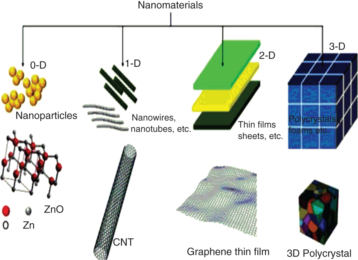
Figure 16.1 Classification of nanomaterials depending on their dimensions resource from B. D. Malhotra [17].
Source: Malhotra and Ali [17].
Graphene is a thin carbon layered material with honeycomb like structure. From last decade, graphene is the most studied material due to their extraordinary properties like high thermal conductivity, high mechanical strength, high optical activity, high charge carrier mobility, and large surface area [19–21]. Due to these properties, graphene made itself serious alternative option to substitute numerous predictable materials for variety applications.
16.4.4.1 Synthetic Methods
2D nanomaterials were synthesized by different methods (Figure 16.2). Some of them are explained briefly as below.
(A) Top‐down approach
- Preparation of nanosized materials through top‐down approaches is one of the fascinating routs in which massiveness materials are converted into nanomaterials. This policy involves physical breaking of larger source material by high energy process. Following are some top‐down synthetic routes which are used for synthesis of nanomaterials.
(a) Laser ablation synthesis
- In this method, larger targeted material in a solvent was incident by very high energy laser. This high energy lasers vaporized the targeted materials and these vaporized material after condensation in solvent produce nanomaterials [22].

Figure 16.2 Top‐down and bottom‐up approaches.
(b) Mechanical milling
- Due to low cost, use of simplicity, and its versatility, this technique is widely used in industry to prepare nanomaterials. In this milling technique, bulky materials are grounded into nanosized material through a strong mechanical shear force [23].
(c) Arc discharge synthesis
- In this process, a high voltage is applied in between two electrodes which are kept closeness to each other in a solution. An electrical breakdown occurs in a solution due to closeness and high potential differences of electrode giving rise to arc discharge which produces ongoing plasma discharge. Due to this, local temperature increases up to 1000 °C which vaporized materials on the electrode surface and these vaporized materials are condensed in the solution giving nanomaterials [24].
- In this method, larger targeted material in a solvent was incident by very high energy laser. This high energy lasers vaporized the targeted materials and these vaporized material after condensation in solvent produce nanomaterials [22].
(B) Bottom‐up approach
- The most important techniques to produce nanomaterials by condensation to amalgamate of atomic vapors and liquids are the bottom‐up or self‐assembly approaches. This approach uses chemical and physical forces. In this technique, basic atoms, or molecules combine to give nanostructures by reducing them. Some of bottom‐up techniques which are used for the synthesis of nanomaterials are as given below.
(a) Sol–gel method
- This is a new technique for the synthesis of multicomponent nanomaterials by controlling the reaction conditions throughout the synthesis. By using this solid homogeneous method powder, metal oxides, and mixed metal oxide nanoparticle were synthesized at lower processing temperature. This technique involves preparation of metal ions solution which is converted into gelatin and after the final product. During this conversion, hydrolysis, polycondensation, gelation, drying, and heating steps occur. Sol–gel technique is a very important technique due to its lower processing temperature, control of substituent concentration, high purity, and homogeneity [25].
(b) Hydrothermal method
- It involves preparation of huge scale nanomaterials at high temperature and pressure by dissolving minerals in hot water. The synthesis is carried in a suitable steel vessels called as autoclave. In this technique, the rise of temperature is sustained among two contrary ends of expansion chamber. During this route chemical precursor is break down at warm end and seed crystals are settled at cooler end. It is useful to prepare large amount of best quality nanocrystalline phase of crystals [26].
(c) Chemical vapor deposition (CVD)
- It is one of the important techniques for the deposition of films of solid materials through vapor phase by decomposition of chemicals on the substrate surface. The obtained material is in the form of thin films, single crystal, or powder. The physical and chemical properties of material are improved by varying experimental conditions like substrate temperature, substrate material, and their concentration, used reaction gas mixtures composition, and pressure of gas flow. Chemical vapor deposition (CVD) technique is applied in many thin films applications such as conductors, conductive oxides, heat‐resistant coating, solar cells, and dielectrics [27].
16.5 Characterization Techniques for 2D Nanomaterials
The prepared nanomaterials are characterized by different techniques; some of them are as given below
- Phase formation temperature is analyzed by thermo‐gravimetric and differential thermal analysis (TG/DTA).
- Structural analysis is studied using X‐ray diffraction technique (XRD).
- Purity and phase composition is studied by energy dispersive X‐ray analysis (EDAX).
- Morphological and micrographic analysis is carried by scanning electron microscope (SEM).
- Atomic force microscopy (AFM) and scanning tunneling microscope (STM) are used to study and adapt nano‐objects.
- Microstructure and particle size is analyzed by transmission electron microscopy (TEM).
- X‐ray photoelectron spectroscopy (XPS) is used to measure elemental composition, empirical formula, chemical state, and electronic state of the material.
- Diffuse reflectance spectroscopy (DRS) is used to study optical properties of the nanomaterials.
- Infra‐red spectroscopy is used to study metal oxides bond stretching frequency.
- Vibrating sample magnetometer (VSM) is used to study magnetic properties of the nanomaterials.
- DC electrical resistivity and thermo‐electric power (TEP) measurements are used to investigate conducting behavior and type of semiconductor, respectively.
- Nanomaterials are also used to study photocatalytic activity.
- These prepared materials are also used to study and carry out different organic reactions.
16.6 Applications of 2D Nanomaterials
Nanomaterials have small particle size and higher catalytic activity; it has wide applications in different fields like
- Medicine: It is used in medicine to deliver drugs, diagnostic applications, protein chips, gene delivery, tools in imaging and biopharmaceuticals, etc.
- Green nanotechnology: This technology described the reduction of environmental and human health risks by developing clean technologies. For example, treatment of pollution, saving fuels, desalinate water, and making solar cells with most cost efficient
- Energy applications: Using nanotechnology, we generate new proficient and cost‐effective energy, such as electricity generated from windmills and waste heat solar economy, biofuels, thermoelectricity, and hydrogen energy.
- Industrial applications: Nanomaterials are used in variety of industry for different purpose, such as consumer goods, agriculture, oil and gas, food, chemical, construction, and aerospace,.
- Nanoelectronics: It mentions the use of nanotechnology in electronic component, i.e. radios, computers, displays, memory storage, quantum computers, optoelectronic devices, energy production, cell phones, etc.
- Nanotechnology in warfare: Nanomaterials are specially used in defense and warfare area such as bullet‐proof vests, nano‐helmets, chemical weapons, biological weapons, nuclear weapons, nanosensors, small satellites, and nano bomb.
- Carbon nanotube: These are the conventional composite materials; due to their electrical, mechanical, and thermal barrier, they are widely used in future transport, biomedical, environmental remedial, structural, daily life material, electrical, and sustainable energy.
16.7 Photocatalytic Application
16.7.1 Why Photocatalyst?
Water is one of the most essential things for all living organism for survival. World is surrounded by 70% of water, out of these only 3–4% is fresh water available on all over the earth in the form of river, ponds, and streams, and remaining is the saline water. This fresh water is polluted by direct discharge of wastewater from different industry and some area human activity also. This wastewater contains different heavy metal ions as well as organic pollutants like dyes and phenols which are most hazardous and highly toxic to the human and environment. So removal of these hazardous materials from wastewater is becoming a serious case [28].
Recently, the organic and biological pollutants from water can be removed by applying chlorination and ozonization process. These active oxidizing agents quickly react with different natural organic compounds in water and produced different carcinogenic by‐products. With this, due to development of resistance power of some organisms toward chlorine they require higher doses than normal for complete inactivation. Physical disinfection and ultraviolet (UV) irradiation technique is also used for water treatment technology. But unluckily UV irradiation technique is also unacceptable for definite kinds of microbes. Therefore, it is essential to develop sustainable water disinfections technique to remove pathogens from water [29].
16.7.2 Brief History of Photocatalysis
The scientific and engineering interest in the application of semiconductor photocatalysis has grown exponentially in the last 10 years. Semiconductor photocatalysts have attracted much attention in the past decade because of their potential applications in the removal of all kinds of pollutants in air or water. Most of the investigations have focused on mixed‐metal oxides which show relatively high reactivity and chemical stability under UV light. The photocatalytic degradation of organic molecules is of great importance in water treatment. In most cases, dyes are studied as model compounds for large organic molecules [30].
The heterogeneous photocatalysis is a useful option in the highly developed researches for both disinfection and decontamination of water. It has high photochemical stability and utilizes solar light for irradiation of water treatment effectively. The good photocatalysts must have good crystallinity, non‐toxicity, easiness in handling, inexpensive applicability, cheapness, high surface area, etc., and should not produce toxic by‐products [31].
Nowadays, 2D nanomaterials due to their unique electronic, optical, biosensing, and physicochemical properties attracted attention of researchers and used as an excellent photocatalyst for degradation of variety of dyes. Currently, nanomaterials of graphene and their derivatives are widely used as heterogeneous photocatalyst in different areas, particularly for water purification and disinfections due to their large surface area, high charge carrier mobility, high mechanical stiffness, and its biocompatible nature.
16.7.3 Principles of Heterogeneous Photocatalysis
The basic principle of photocatalysis process is a semiconductor photo excitation as a result of radiation absorption, normally near UV spectrum. Under near UV irradiation, a suitable semiconductor material may be excited by photons possessing energies of sufficient magnitude to produce conduction band electrons and valence band holes which are shown in Figure 16.3. These charge carriers are able to induce reduction or oxidation, respectively, and react with both water and organic compounds. The holes are extremely oxidants and should thus be able to oxidize almost all chemicals, as well as water, resulting in the formation of hydroxyl radicals [33–35]. Meanwhile, holes react with donors (H2O, OH−) to produce oxidant species. Oxidant species produced from electrons and holes have strong oxidizing abilities and can directly oxidize organic compounds into CO2 and H2O [36, 37].
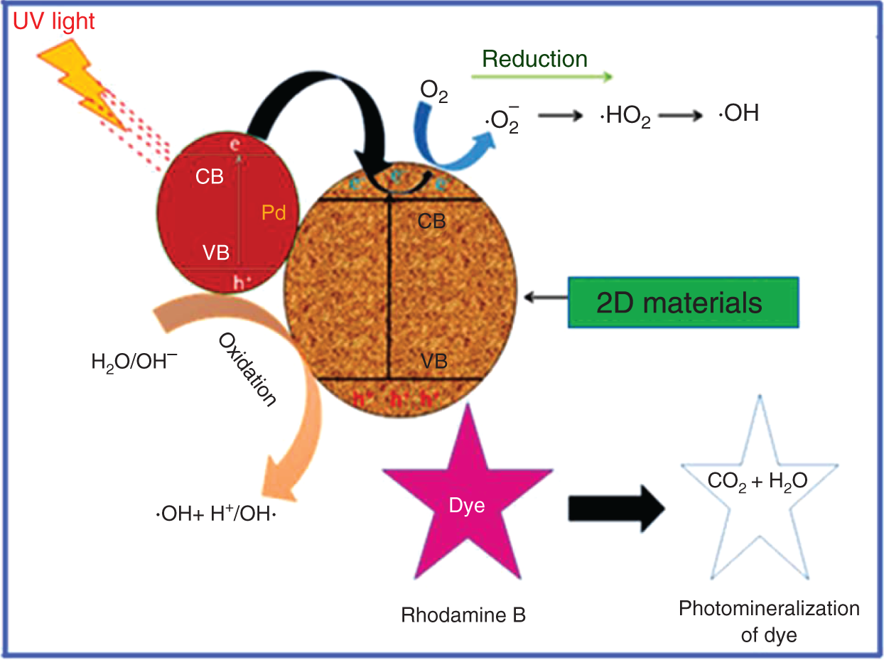
Figure 16.3 Principles of photocatalysis showing the energy band gap diagram.
Source: Patil et al. [32].
16.7.4 Photocatalytic Study of 2D Nanomaterials
Recently, Yue Liu et al. [38] studied the photocatalytic activity of 2D nanomaterials toward water disinfection and their progress and future challenges. In this review article, they ordered 2D nanomaterials as structural brick for photocatalytic water disinfections. They mentioned five groups of 2D nanomaterials such as graphene, 2D metal oxides and metallates, graphitic carbon nitride, transition metal dichalcogenides, and metal oxyhalides for photocatalytic pathogens inactivation. Pardeep Singh et al. [39] had mentioned different plans for improvement of photocatalytic activity of graphene‐based nanocomposites for water purification. In this review article, they summarized several works finished on the usage of graphene‐based photocatalytic system in water purifications. Priyanka Ganguly et al. [40] carried out study on 2D nanomaterials for photocatalytic hydrogen production. In this article, they explained current progress made in photocatalytic hydrogen evolution reaction by 2D nanomaterials and composite heterostructures. They also mentioned fresh perception on the scenario and challenges obtained behind the applications and synthetic strategies. Mohammad Tahir et al. [41] studied tubular graphite–C3N4 materials for energy storage and green photocatalyst. They synthesize graphitic carbon nitride (g‐C3N4) by chemical method and it is used as an electrode material for super capacitors in KOH electrolyte first time. The obtained results are higher than that of earlier reported. They also used g‐C3N4 as a good photocatalyst for degradation of methyl orange (MO) and methyl blue (MB) dye. Jing Sun et al. [42] fabricated 0D–2D BiVO4 nanoparticles/reduced graphene oxide, 1D–2D BiVO4 nanotubes/reduced graphene oxide nanocomposites, and 2D–2D BiVO4 nanosheets/reduced graphene oxide nanocomposites heterojunction photocatalyst by solvothermal process. Their reading promotes new progress in dimensionally factors on manipulating the heterojunction photocatalyst for photodegradation and photocatalytic applications in environmental issue. Xiu Wang et al. [43] were synthesized ternary hybrid structured material of Fe0 doped GCN/MoS2 layered structure network by facile method. The prepared materials were used for photocatalytic degradation of RhB dye and for reduction of Cr(VI). With this, there are also so many other review and research articles which were focused on photocatalytic degradation and disinfection of water by 2D nanomaterials.
16.7.5 Challenges Behind 2D Nanomaterials as a Photocatalyst
Nowadays, 2D nanomaterial becomes increasing demands due to its wide applications in different fields. But it also raised some matter regarding its probable toxicity. Due to very small particle size, TiO2 nanoparticles cause lung inflammation [44]. Singh et al. [45] reported the risk of DNA injury resulting in afterword cancer growth. While variety modes of photocatalyst cause cell death have been proposed depending on impact of reacting species and the method of cell apoptosis, the accurate mechanism is immobile under further research [38]. Some of the researchers mentioned 2D‐based nanomaterials for antibacterial photocatalysis which focused on enhanced charge partition and reactive species production. In this study, main issue is how 2D materials interact with pathogenic cells; persuasive confirmation and clarification are still lacking [38].
References
- 1 Xiangfeng, C., Dongli, J., and Chenmou, Z. (2007). Sens. Actuators, B 123: 793.
- 2 Harris, V.G., Geiler, A., and Chen, Y. (2009). J. Magn. Magn. Mater. 321 (14): 2035.
- 3 Wang, Y.C., Ding, J., Yi, J.B. et al. (2004). Appl. Phys. Lett. 84: 2596.
- 4 Mozaffari, M., Amighian, J., and Darsheshdar, E. (2014). J. Magn. Magn. Mater. 350: 19.
- 5 Ozin, G.A. and Arsenault, A.C. (2005). Nanochemistry: A Chemical Approach to Nanomaterials. London: Royal Society of Chemistry.
- 6 Gotic, M., Czako‐nagy, I., Popovic, S., and Music, S. (1998). Philos. Mag. Lett. 78: 193.
- 7 Shinde, A.B. (2013). Int J. Innovation Tech. Explor. Eng. 3: 4.
- 8 Misra, R.D.K., Kale, A., Kooi, B.J., and De Hosson, J.T.M. (2003). J. Mater. Sci. Technol. 19: 1617.
- 9 Abad, E. et al. (2005). Nano Dictionary. Basel: Collegium Basilea.
- 10 Gleiter, H. (2000). Acta Mater. 48: 1.
- 11 Skorokhod, V., Ragulya, A., and Uvarova, I. (2001). Physico‐chemical Kinetics in Nanostructured Systems, 180. Kyiv: Academperiodica.
- 12 Pokropivny, V.V. and Skorokhod, V.V. (2007). Mater. Sci. Eng., C 27: 990.
- 13 Chen, H., Cong, T.N., Yang, W. et al. (2009). Prog. Nat. Sci. 19: 291.
- 14 Geng, X. and Yi, J. (2019). Nano‐Sized Multifunctional Materials. Elsevier B.V.
- 15 Shinde, P.V. and Singh, M.K. (2019). Fundamentals and Sensing Applications of 2D Materials, 91–143. Bangalore, India: Elsevier, Indian Institute of Science.
- 16 Late, D.J., Bhat, A., and Rout, C.S. (2019). Fundamentals and Sensing Applications of 2D Materials, 5–24. Cambridge, MA: Woodhead Publishing.
- 17 Malhotra, B.D. and Ali, M.A. (2018). Nanomaterials for Biosensors. Elsevier B.V.
- 18 Geim, A.K. (2012). Phys. Scr. 146: 014003.
- 19 Pradhan, D. and Leung, K.T. (2008). J. Phys. Chem. C 112: 1357.
- 20 Tiwari, J.N., Pan, F.M., Tiwari, R.N., and Nandi, S.K. (2008). Chem. Commun. 37: 6516.
- 21 Nayak, B.B., Behera, D., and Mishra, B.K. (2010). J. Am. Ceram. Soc. 93: 3080.
- 22 Vinceno, A. and Moreno, M. (2009). Phys. Chem. Chem. Phys. 11 (20): 3805–3821.
- 23 Nunes, D. and Martins, R. (2019). Metal Oxides Nanoparticles, 21–57. Elsevier.
- 24 Lijima, S. (1991). Nature 354: 56–58.
- 25 Sanadi, K.R. and Kamble, G.S. (2017). Adv. Porous Mater. 5: 1–4.
- 26 Ulrich, S. and Nicola, H. (2012). Synthesis of Inorganic Materials, 161. Weinheim: Wiley‐VCH.
- 27 Shareef, I.A., Rubloff, G.W., Anderle, M. et al. (1995). J. Vac. Sci. Technol., B 7: 01.
- 28 Pelaez, M., Nolan, N.T., Pillai, S.C. et al. (2012). Appl. Catal., B 125: 331–349.
- 29 Antonopoulou, M., Evgenidou, E., Lambropoulou, D., and Konstantinou, I. (2014). Water Res. 53: 215–234.
- 30 Ghalya, Y.M. et al. (2006). Chem. Eng. J. 145: 51.
- 31 Andreozzi, R., Caprio, V., Insola, A., and Marotta, R. (1999). Catal. Today 53: 51.
- 32 Patil, S.P., Sanadi, K.R., and Helavi, V.B. (2017). J. Mater. Res. 20 (6): 1445.
- 33 Kummerer, K. (2004). J. Antimicrob. Chemosphere 54 (2): 311.
- 34 Rauf, M.A. and Salman Ashraf, S. (2009). Chem. Eng. J. 151: 10.
- 35 Valenzuela, M.A., Bosch, P., Jimenez‐Becerrill, J. et al. (2002). J. Photochem. Photobiol., A 148: 177.
- 36 Zhang, L., Zhou, X., Guo, X. et al. (2011). J. Mol. Catal. A: Chem. 335: 31.
- 37 Zhang, H., Chen, G., and Bahnemann, D.W. (2009). J. Mater. Chem. 19: 5089.
- 38 Liu, Y., Xeng, X., Hu, X. et al. (2018). J. Chem. Technol. Biotechnol. 94: 1.
- 39 Singh, P., Shandilya, P., Raizada, P. et al. (2020). Arabian J. Chem. 13: 3498–3520.
- 40 Ganguly, P., Harb, M., Cao, Z. et al. (2019). ACS Energy Lett. 4: 1687–1709.
- 41 Tahir, M., Cao, C., Butt, F.K. et al. (2013). J. Mater. Chem. A 1: 13949–13955.
- 42 Sun, J., Wang, C., Shen, T. et al. (2019). Nanomaterials 9: 907.
- 43 Wang, X., Hong, M., Zhang, F. et al. (2016). ACS Sustainable Chem. Eng. 4: 4055–4063.
- 44 Grassian, V., O'Shaughnessy, P., Adamcakova‐Dodd, A. et al. (2007). Environ. Health Perspect. 115: 397–402.
- 45 Singh, N., Manshian, B., Jenkins, G. et al. (2009). Biomaterials 30: 3891–3914.