18
2D Dichalcogenides
Ram S. Singh1, Varun Rai2, and Arun K. Singh3
1O. P. Jindal University, Department of Physics, Punjipathra, Raigarh, Chhattisgarh, 496109, India
2Nanyang Technological University, School of Materials Science and Engineering, Block N4.1, 50 Nanyang Avenue, 639798, Singapore
3Guru Ghasidas Vishwavidyalaya, Department of Pure & Applied Physics, Bilaspur, Chhattisgarh, 495009, India
18.1 Introduction
Two‐dimensional (2D) dichalcogenides have emerged as a fascinating area of research and development in recent years due to their outstanding properties [1–6]. The commonly studied 2D dichalcogenides are molybdenum disulfide (MoS2), molybdenum diselenide (MoSe2), molybdenum ditelluride (MoTe2), tungsten disulfide (WS2), tungsten ditelluride (WTe2), and tungsten diselenide (WSe2) [7]. However, the most studied material in this family is MoS2 due to its robustness. 2D dichalcogenides have potential applications in almost all areas including optoelectronics, sensors, spintronics, photocatalysis, and biomedical [7].
Dichalcogenides have an interesting history. Linus Pauling first determined the crystal structure of bulk MoS2 in 1923 [8]. Later in the 1960s, several dichalcogenides were known with layered structures [9]. Robert Frindt [10] first reported the exfoliation of ultrathin MoS2 layers by adhesive tapes in 1963. Subsequently, single layer (SL) MoS2 suspensions were first produced in 1986 [11]. The discovery of graphene in 2004 [12] and the rapid growth of research in this area opened an avenue to new studies of other 2D materials. In particular, the absence of an electronic band gap in graphene has stimulated the research for 2D dichalcogenides with the semiconducting property such as MoS2 and WS2.
This book chapter focuses on many important aspects of 2D dichalcogenides. Beginning with a short introduction, structure and properties of 2D dichalcogenides, their different synthesis techniques, and various potential applications have been well documented.
18.1.1 What Are 2D Dichalcogenides?
Atomic structure of 2D dichalcogenides is layered having very strong in‐plane bonding. However, the layered structure can be exfoliated in 2D sheets due to weak van der Waals interactions between the layers. MX2 is the general chemical formula for 2D dichalcogenides, where M represents a transition metal element from group IV (Ti, Zr, Hf, etc.), group V (V, Nb, or Ta), or group VI (Mo, W, etc.) and X represents a chalcogen (S, Se, or Te) [7, 13]. The structure X–M–X is formed when the M atoms are sandwiched covalently between two X atoms. Since these materials involve transition metals so named as transition metal dichalcogenides (commonly abbreviated as TMDCs). By the stacking of X–M–X through van der Waals interactions, the bulk TMDCs are shaped. Because of variations in stacking orders and transition metal atom coordination, several structural phases of TMDCs exist. The crystal structure of TMDCs has different polytypes such as 2H, 1H, 1T, and 3R. However, the 2H (trigonal prismatic coordination) and 1T (octahedral coordination) are the two common structural phases as shown in Figure 18.1. The 2H phases are formed by ABA stacking in which X atoms in different atomic planes occupy the same position A and located on top of each other in the direction normal to the layer. On the other hand, there is an ABC stacking order in the 1T phases. These structural changes are directly related to the physical properties of materials. The 2H and 1T phases are thermodynamically stable, while other phases are metastable.

Figure 18.1 Different polytypes ((a)–(c), 2H, 3R, and 1T) of TMDCs. Here a presents lattice constant (3.1–3.7 Å), c presents stacking index and the interlayer distance is around 6.5 Å.
Source: Wang et al. [13].
18.1.2 Properties
2D dichalcogenides exhibit various captivating properties that include superior optical, electronic mechanical, thermal, and superconducting properties. Owing to these interesting properties, these materials can be considered for the substitution of silicon in several areas that include electronics, optoelectronics, photonics, and nanoelectromechanical systems (NEMS).
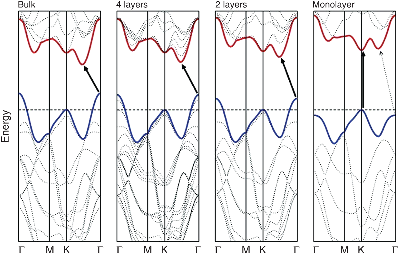
Figure 18.2 Changes in energy band structure of 2H MoS2 material from bulk through few layers to monolayer.
Source: Splendiani et al. [17].
Based on the coordination of the metal atoms in dichalcogenides and the oxidation state, they possess electrical properties ranging from insulators (hafnium disulfide: HfS2) through semiconductors (MoS2 and WS2) to semimetals (titanium diselenide: TiSe2 and tungsten ditelluride: WTe2) and true metals (vanadium diselenide: VSe2 and niobium diselenide: NbSe2) [14–16]. Bulk dichalcogenides in their 2H form have an indirect band gap. The indirect band gap values are 1.3–1.4 eV for WS2, 1.0–1.29 eV for MoS2, 1.1 eV for MoSe2, and 1.2 eV for WSe2. On the other hand, a monolayer of these materials shows direct band gap with values 1.8–2.1 eV for WS2, 1.8–1.9 eV for MoS2, 1.5–1.6 eV for MoSe2, and 1.6–1.7 eV for WSe2. The evolution of the electronic energy band structure of MoS2 from bulk to monolayer is presented in Figure 18.2. With respect to the bulk, monolayer shows a significant change in electronic structure with an increased band gap. This effect is attributed to the quantum confinement [17, 18]. The conduction band minimum (CBM) and the valence band maximum (VBM) in MoS2 are formed due to the hybridization of S 3p and Mo 4d orbitals.
Among the 2D dichalcogenides family, semiconductor 2D dichalcogenides having outstanding optical properties are of much interest. 2D dichalcogenides show optical absorption in the visible and near infrared (NIR) spectral range. This absorption is caused by the direct band‐to‐band transitions (Figure 18.3). The sharp resonance peaks (presented as a solid green curve in Figure 18.3) in the absorption spectrum are originated due to the excitonic transitions. If there is no excitonic effect, the absorption spectrum shows a step‐function‐like curve (presented by the blue line in Figure 18.3). This step‐function‐like curve is evolved from transition matrix elements and the energy‐independent joint density of states near band edges [19].

Figure 18.3 Optical absorption spectrum recorded from single layer MoS2 at a low temperature of 10 K (indicated by green curve) with A and B as exciton peaks. The spectrum indicated by the blue dashed curve exhibit no excitonic effect. The generation of a bound exciton under illumination is presented in the inset.
Source: Mak and Shan [19].
Monolayer dichalcogenides show a very strong excitonic effect with very high binding energies 0.5–1.0 eV [19]. Besides exciton, biexciton (that is bound states of two excitons) and trion (that is bound state of one hole and two electrons, or two holes and one electron) also exist in undoped and doped SL dichalcogenides, respectively. 2D dichalcogenides have much larger excitonic binding energy (about an order of magnitude larger) than that of conventional 2D semiconductors, which make these materials unique for room temperature applications. Importantly, the larger the exciton binding energy the shorter will be the lifetime. These optical properties that include strong absorbance, the high exciton binding energy and small lifetime play important roles in 2D dichalcogenides for photonic and optoelectronic applications.
2D materials generally show high mechanical strength which can further be tailored by the incorporation of topological defects and out of plane deformation. Most of the 2D materials show negative Poisson's ratio, which is opposite to the positive Poisson's ratio of conventional materials. Materials having negative Poisson's ratio show a transverse contraction if they are compressed and a transverse expansion if they are stretched in the longitudinal direction. It has been reported that MoS2 has outstanding ductility. Besides, high breaking strength ∼23 GPa and large Young's modulus ∼300 GPa have been demonstrated in an SL MoS2 [20].
2D materials such as graphene [21] and hexagonal boron nitride [22, 23] have also gained considerable attention due to their superior thermal properties. However, thermal conductivities of 2D dichalcogenides are relatively low due to the short mean free path and phonon group velocity [24]. Monolayer WS2 has the highest thermal conductivity of 113.97 W/mK at 300 K, while WTe2 monolayer has the lowest thermal conductivity of 33.66 W/mK at 300 K as predicted by theoretical studies [25]. Interfacial thermal conductance in 2D dichalcogenides‐based devices is improved by connecting these materials to other materials such as graphene and metal electrode with chemical bonds.
Superconductivity is another interesting property studied in 2D materials. The superconducting state in dichalcogenides is found intrinsically and it can also be induced by electrostatic doping, chemical doping, or applied pressure. All bulk dichalcogenides (except 2H–SbN2, which is only superconducting) showing a charge density wave (CDW) state are superconductors. The CDW and superconducting state can either coexist or compete. The superconducting property of bulk dichalcogenides sustains in their 2D structure as well. Monolayer 2H–NbSe2 shows intrinsic superconductivity at the critical temperature of 3 K. 2D 2H–MoS2, 2H–WS2, and 2H–MoSe2 have shown the superconducting state under the application of electrostatic gating [26].
18.2 Methods of Synthesis
Various synthetic strategies have been used so far to synthesize high‐quality (i.e. tuning thickness, lateral dimensions, crystallinity) mono‐ and few‐layer (FL) TMDCs in large amounts for application purposes. All the synthetic strategies can be categorized into either “top‐down” or “bottom‐up” methods. Top‐down methods involve achieving few and monolayered nanomaterials through different exfoliation techniques from bulk crystals and bottom‐up methods follow using precursors such as atoms/molecules to grow into layered nanomaterials under optimized conditions.
18.2.1 Top‐Down Method
18.2.1.1 Micromechanical Exfoliation
Bulk TMDCs crystals have weak van der Waals bonding between layers and strong covalent bonding among atoms at the same layer. The weak van der Waals bonds in the crystal lattice are overcome by applying shear forces to the bulk crystal that results in producing thinner layered TMDCs and subsequent repeating the thinning process of TMDCs flakes leads to eventually SL nanosheet. Lamellar TMDCs are exfoliated micromechanically by compressive delamination, shear‐induced separation, or applying peeling force to detach the layers. The scotch‐tape method has been widely used to obtain few layers and a single TMDC nanosheet from lamellar crystals. The lamellar crystals are placed between two pieces of adhesive scotch tape in the scotch‐tape method and both tapes are peeled apart to cleave the crystal. This process is repeated on freshly peeled flakes to obtain even few layers and SL nanosheet, transferable over a substrate for characterizations and fabrication of devices [27]. 2D transition metal dichalcogenides (2D TMDCs) prepared by mechanical exfoliation are highly crystalline nanosheets with few defects. The highly crystalline nanosheet samples are needed for the fundamental exploration of intrinsic physicochemical properties and applications in electronic devices. However, large amount of production, controlling the thickness and size of the 2D TMDCs flakes, is extremely critical by this method, and the substrate is required to support the nanosheet. Moreover, these 2D TMDCs do not meet the requirement of biomedical applications [28].
18.2.1.2 Liquid Exfoliation
Liquid exfoliation involves applying a vibrational energy or cavitation forces to the bulk TMDCs crystals in the specific solvent by ultrasonication. Later, dispersed, exfoliated TMDCs nanosheets are separated from the unexfoliated crystal by centrifugation [27]. In this method, suitable ultrasonic intensity and time duration are very important to break the weak van der Waals forces between interlayers to obtain the desired exfoliation (thickness of flakes) from the TMDCs crystals. The solvent molecules in liquid exfoliation play an important role in stabilizing the exfoliated flakes and preventing their reassembly. The surface free energy between solvent molecules and exfoliated nanosheets should properly match to obtain enhanced exfoliation efficiency. Liquid exfoliation of TMDCs crystals is suitable for the mass production of ultrathin and FL sheets with good photoelectric properties; however, it remains challenging to achieve SL 2D‐TMDCs. Moreover, this method involves commonly organic solvents such as dimethylformamide (DMF) and N‐methyl‐pyrrolidone (NMP). Thus, improvement in experimental condition, i.e. the toxicity of organic solvents is an important area for current research in this area for industrial applications.
18.2.1.3 Chemical Intercalation and Exfoliation
The intercalator molecules such as naphthyl sodium, butyl lithium, etc., are used to be intercalated between the interlayer of the bulk TMDCs crystals for exfoliation by ultrasonication in water or ethanol [29]. Intercalation of intercalator (small size molecules) between the interlayer of TMDCs crystal leads to increased interlayer spacing and reducing the van der Waals forces, which results in TMDCs nanosheet dispersion during ultrasonication. Li intercalation into the crystals of MoSe2, MoS2, WSe2, and WS2 follows electron transfer and subsequent Li+ ions coordination leading to reduction of TMDCs crystals into ![]() [30], that reacts with water to remove formal charge within the nanosheets and the metal cations to exfoliate MX2 as neutral nanosheets. Chemical exfoliation based on intercalation avoids the usage of toxic organic solvents and has been used to synthesize various 2D TMDCs that can be used in biomedical applications.
[30], that reacts with water to remove formal charge within the nanosheets and the metal cations to exfoliate MX2 as neutral nanosheets. Chemical exfoliation based on intercalation avoids the usage of toxic organic solvents and has been used to synthesize various 2D TMDCs that can be used in biomedical applications.
18.2.1.4 Electrochemical Exfoliation
Electrochemical exfoliation of TMDCs crystals is carried out to obtain monolayer and FL 2D TMDCs nanosheets. Electrochemical exfoliation of MoS2 is carried out in electrolyte of 0.5 M Na2SO4 solution, using bulk MoS2 crystal and Pt wire as working and counter electrode, respectively. Positive bias is applied at the working electrode to exfoliate the crystal of bulk MoS2 immersed in the electrolyte. In this process, **•˙OH and ˙O radicals produced by the oxidation of the water molecules and SO42− insert between the MoS2 interlayers and reduce the interlayer van der Waals forces [20, 31]. Subsequent oxidation of the trapped radicals and/or anions release SO2 or O2 gas, resulting in the expansion of the layers and detachment of the flakes from the crystal. Electrochemical exfoliation produces MoS2 sheets in the range of 5–50 μm, larger size than chemical or liquid‐exfoliation methods. The surface oxidation of bulk 2D‐TMDCs crystal is critical, which should be avoided during electrochemical exfoliation by optimizing the experimental conditions to obtain high‐quality 2D TMDCs flakes.
18.2.1.5 Thinning by Thermal Annealing, Laser, and Chemical Etching
Thinning of pre‐exfoliated nanosheets is carried out by thermal annealing, scanning laser, and chemical etching to meet the application requirement of the samples. Thermal annealing and scanning laser cause sublimation of the upper layer and leaving the layers underneath intact, due to the adsorption of thermal energy within the interlayers of the nanosheets. The chemical etching agent XeF2 has been used to do thinning of MoS2 by promoting oxidation on the surface followed by layer‐by‐layer thinning of the sheets in a time‐controlled reaction [32]. However, chemical etching leads to surface roughening.
18.2.2 Bottom‐Up Method
18.2.2.1 Chemical Vapor Deposition
In chemical vapor deposition (CVD), the reaction precursors decompose or react or deposit as FL or monolayer film on the exposed substrate under high temperature and pressure [33–37]. The reaction precursor provides chalcogenide atoms and transition metal atoms for facilitating reaction to form thin‐layered 2D TMDCs over an exposed substrate. 2D TMDCs nanosheets prepared by CVD show high‐quality crystal with excellent electronic property and improved transfer process of nanosheets due to utilization of the substrate. However, high temperatures and high vacuum conditions are required in the CVD process. The CVD process can be categorized into four synthetic methods. Figure 18.4 (a–d) shows four different synthetic methods in the CVD process for the growth of 2D TMDCs. (i) The first synthetic method involves thermal decomposition where precursor molecules containing both chalcogen and metal atoms e.g. (NH4)2MoS4 are decomposed under reducing and the inert environment in the presence of H2 at low temperature. The reducing environment in this process prevents oxidation and (NH4)2MoS4 precursor molecules convert directly into MoS2. (ii) The second method is based on sulfurization/selenization/tellurization of pre‐deposited metal oxide or metal films on a suitable substrate. In this method, metal or metal‐containing precursors are deposited by spin coating, e‐beam evaporation, thermal evaporation, and atomic layer deposition (ALD). (iii) The third method involves the physical vapor transport method where TMDCs powder e.g. MoS2 is placed at high temperature zone (∼900 °C) and used as a precursor for growing high‐quality FL and monolayer TMDCs via vapor solid growth mechanism under Ar gas, on an insulating substrate placed at relatively cooler zone, ∼650 °C. (iv) The fourth synthetic method of CVD involves vapor phase reaction between transition metal oxides/halides and chalcogen precursors. This vapor phase reaction of the CVD process is further categorized according to specific condition used such as modified metal–organic CVD (MOCVD), atmospheric pressure CVD (APCVD), and low‐pressure CVD (LPCVD) (shown in Figure 18.4d).
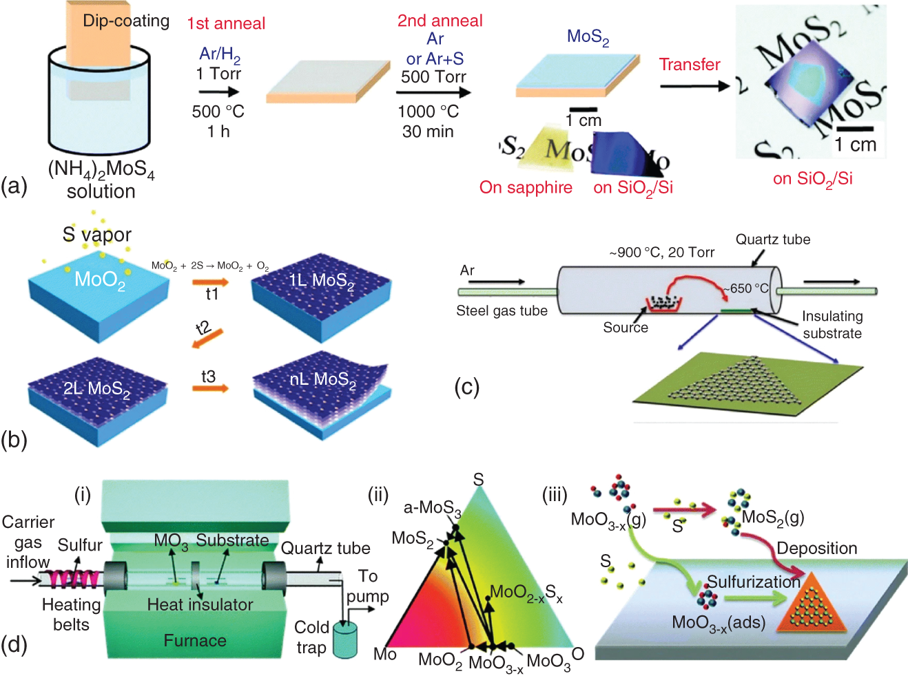
Figure 18.4 Four different synthetic methods in the CVD process for the growth of 2D TMDCs [34]. (a) Thermal decomposition of (NH4)2MoS4 under reducing and inert environment into MoS2.
Source: Reprinted with permission Liu et al. [33], (copyright 2012) American Chemical Society. (b) Surface sulfurization of pre‐deposited metal oxide MoO3 to obtain the layered deposition of MoS2.
Source: Wang et al. [35]. (c) The physical vapor transport method of MoS2 films formation on an insulating substrate under inert gas atmosphere, where MoS2 powder is placed at high temperature zone and the insulating substrate placed at a relatively cooler zone.
Source: Wu et al. [36]. (d) (i) LPCVD system setup for TMDCs, (ii) Mo–O–S ternary phase diagram showing the CVD growth pathways of MoS2 from MoO3 precursors, and (iii) possible growth routes of MoS2 by the reaction of MoO3−x and S.
Source: Ji et al. [37].
18.2.2.2 Solvo‐Thermal
Ultrathin 2D TMDCs are prepared from precursors in solvo‐thermal method by applying specific reaction condition (solvent, heating, and reaction time) [38, 39]. Molybdic acid or tungstic acid reacts with thiourea at 773 K for three hours to form ultrathin MoS2 or WS2 nanosheets. This method is useful and relatively inexpensive for mass production of ultrathin 2D TMDCs, however, getting an SL nanosheet remains challenging. Ultrathin 2D TMDCs nanosheets show high surface energy due to high aspect ratio (surface area‐mass ratio) and a large number of atoms exposed outside. Therefore, surface modification of 2D TMDCs is carried out to minimize surface energy, improving the stability and dispersibility by physical adsorption (e.g. hydrophobic interaction, electrostatic attraction, and van der Waals force) and chemical bonding (e.g. covalent bond or coordination bond) for potential various applications.
18.2.2.3 Molecular Beam Epitaxy
Molecular beam epitaxy is a scalable method to grow 2D TMDCs with atomic monolayer thickness control. In this method, an ultrahigh vacuum chamber with pressure typically below 10−10 mbar is used with several precursor molecule sources (e.g. Ga, Se) for molecular beams to deposit on a preheated substrate while simultaneously in situ monitoring the thickness and substrate crystallinity using reflection high‐energy electron diffraction and low‐energy electron diffraction [26].
18.3 Modification of Properties
For the development of semiconductor 2D TMDCs‐based practical and reliable high‐performance electronic/optoelectronic devices, the modification of charge carrier concentrations of these materials is needed. Any change of carrier concentration alters the position of the Fermi level of the material. Thus, this can be utilized in the alignment of the Fermi level, which is crucial in determining the successful operation of the electronic devices such as field effect transistors (FETs), light emitting diodes (LEDs), diodes, solar cells, etc. [40, 41]. Doping is an easy and the most efficient technique to change the electrical and optical properties of semiconducting material. Nowadays, several approaches such as the deposition of dopant atoms, chemical modification, and absorption of gas molecules have been applied to modulate the electronic properties of 2D TMDCs materials [42, 43]. Electrical properties of mechanically exfoliated multilayer (ML) molybdenum disulfide (MoS2) are tailored by chemical doping and deposition of a thin layer of gold (Au) [44]. Reversible tuning of charge carriers in MoS2 has been achieved by the deep ultra‐violet (DUV) light‐induced doping of MoS2 [45, 46]. In this case, SL, bi‐layer (BL), and FL MoS2 are exposed to nitrogen gas in the presence of DUV light for different exposure times. The shift of the threshold voltage toward the negative gate voltage is observed under exposure to N2 gas with DUV light, indicating the n‐type doping of MoS2. The device is recovered (reversible doping) when exposed to oxygen gas under the DUV light as shown in Figure 18.5. However, the recovery time is different for different layers of MoS2 nanosheets. This method of reversible tuning of charge carriers in MoS2‐based FET under DUV light with the gas flow is stable and efficient [45].
Another strategy to modulate optical, electronic, and optoelectronic properties of 2D TMDCs is strain engineering [47, 48]. Unlike bulk TMDCs that sustain no more than 1% strain, 2D TMDCs can survive with much higher strain. Hence, the high strain sustainability of 2D TMDCs makes properties of these materials amenable to strain engineering. A 1.35% uniaxial tensile strain reduces the band gap ∼100 meV in multilayer WSe2 [47] (see Figure 18.6). The strain is applied using a cantilever sample holder. The substrate (Figure 18.6b) is bent to make the material under strain. The strain in WSe2 can be estimated as ε = (3tδ/2 L2)(1 − (x/L)), where t, L, x, and δ are the thickness of the flexible substrate, the length of the substrate, the distance from the material to the fixed edge of the substrate, and the deflection of the free edge, respectively. The experimental as well as theoretical results of strain engineering are demonstrated in Figure 18.6c. The alteration of optoelectronic properties of 2D MoX2/WX2 lateral heterostructures using density functional theory (DFT) has also been reported [48]. MoX2 and WX2 undergo a monotonous reduction (while valence band and conduction band offsets remain constant) of band gaps under uniaxial strain. The calculations predict that the band gap can be tuned up to ∼1 eV by applying strain up to 12%. The band gap tuning in a lateral heterostructure facilitates electron–hole separation for light detection/harvesting, thereby improving power conversion efficiency (PCE) of optoelectronic devices. For example, the PCE of lateral MoS2/WS2 heterostructure is improved by ∼35% by applying a 4% strain. On the other hand, the PCE increases by ∼15% at the same 4% strain in case of MoSe2/WSe2 lateral heterostructure [48]. Thus, strained 2D TMDC lateral heterostructures could be promising for future development of efficient optoelectronic devices.
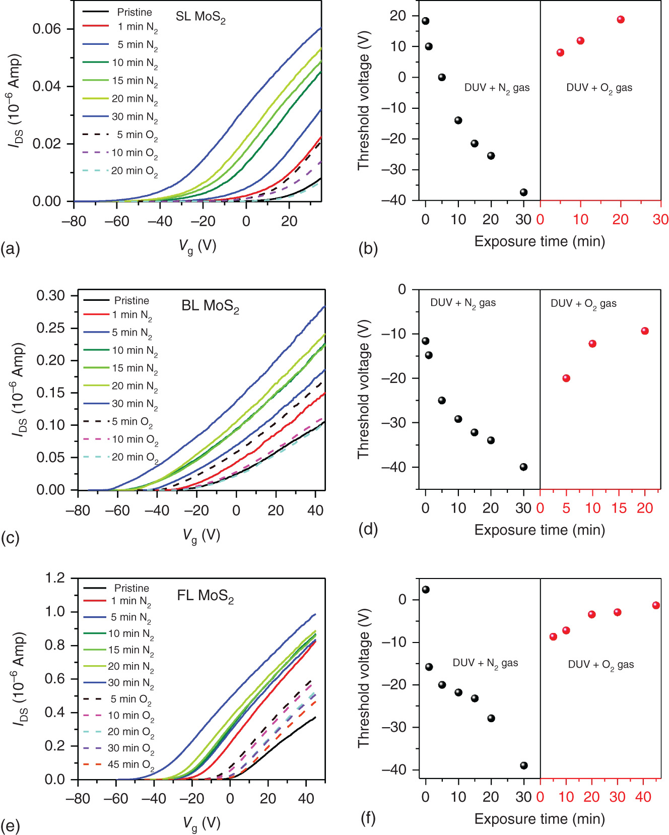
Figure 18.5 Reversible doping of MoS2 by exposing the material to nitrogen (N2) and oxygen (O2) gases under the DUV illumination. (a) Plot of drain current (IDS) versus back gate voltage (Vg) and (b) the variation of threshold voltage as a function of the time of exposure to N2 and O2 gas in the presence of DUV light for SL MoS2. (c) Plot of drain current (IDS) versus back gate voltage (Vg) and (d) the variation of threshold voltage as a function of the time of exposure to N2 and O2 gas in the presence of DUV light for BL MoS2. (e) Plot of drain current (IDS) versus back gate voltage (Vg) and (f) the variation of threshold voltage as a function of the time of exposure to N2 and O2 gas in the presence of DUV light for FL MoS2.
Source: Singh et al. [45]. Here SL = single‐layer, BL = bi‐layer, and FL = few‐layer.
18.4 Applications
18.4.1 Optoelectronics
2D TMTCs have stimulated extensive research interest for the development of optoelectronics in the coming years. The atomic‐level thickness is generally smaller than most particles' transport mean free path, which forces them to follow ballistic transportation rather than scattering or diffusion. It is noticed that 0D (such as quantum dots) and 1D (such as nanowires) nanomaterials suffer from surface dangling bonds and related traps, which may be detrimental for devices. On the other hand, 2D materials have surfaces free from dangling bonds [19], making these materials more applicable in optoelectronic devices. Generally, optoelectronic devices can generate and detect the light and if it is flexible and transparent, then useful for solar cells, wearable electronics, and transparent displays. 2D TMDCs semiconducting materials with direct band gaps are of much interest as they can be effectively utilized in the fabrication of optoelectronic devices. Also, better processability due to the atomically thin structure and band gap tunability of these materials offers advantages over other conventional semiconducting materials. 2D TMDCs have shown applications in various optoelectronic devices including solar cells, LEDs, photodetectors optical switches, and displays. Transparent and flexible optoelectronics are other interesting areas where these materials find potential applications [19].
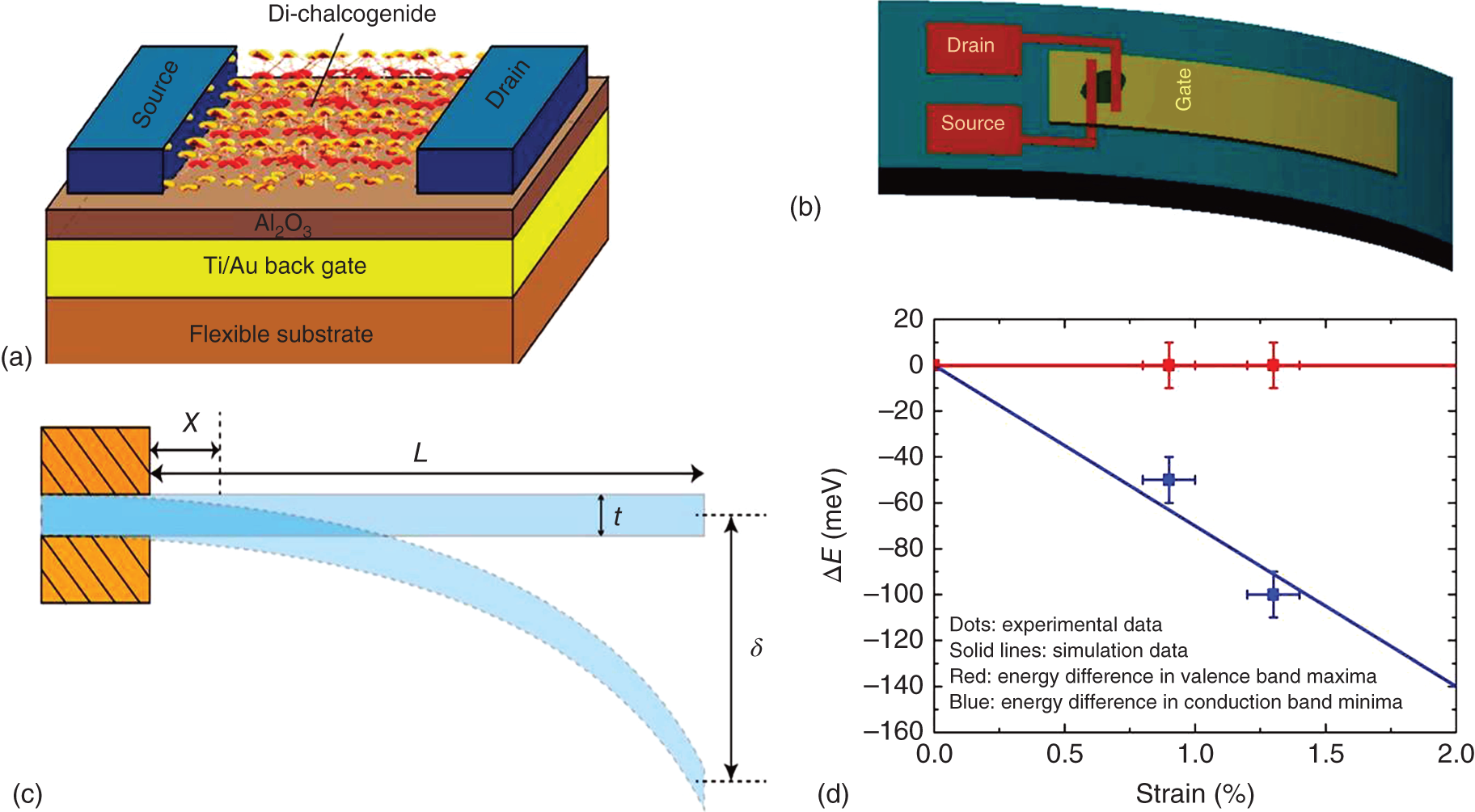
Figure 18.6 Strain engineering of 2D TMDC FET. (a) 2D WSe2‐based FET on a flexible substrate. (b) Bending the device to apply strain. (c) Details of strain calculation. (d) Changes in VBM and CBM under increasing strain.
Source: Shen, Penumatcha, and Appenzeller [47].
18.4.2 Sensors
Sensors have become the necessities of our modern life to monitor and protect the environment and health of humans against toxic chemicals, microorganisms, radiation, and gases. Thus, the development of highly efficient, stable, selective, portable, and low‐power‐consuming sensors is highly demanded [49]. 2D TMDCs material‐based sensors have several attractive features that include high sensitivity, high stability, and compatibility with modern fabrication methods. In addition, the 2D structure of these materials has a large surface area that aids the detection of larger target analysts per unit area with fast response and recovery. Recently, various 2D TMDCs‐based sensors including electrochemical sensors, biosensors, and chemical sensors have been reported [7]. The MoS2 nanosheets exhibit very high sensitivity for NO and NO2 gas; it is better than graphene oxide, carbon nanotube (CNT), and ZnO‐based sensors.
18.4.3 Spintronics
In spintronics, the spin degree freedom of electrons is utilized for novel information storage and logic devices. Graphene as 2D materials with ultra‐low spin orbit coupling is very attractive and one of the most promising candidates for spin devices [50, 51]. 2D TMDCs exhibit a unique spin‐valley coupling that has got a great potential for the intensive research work in spintronics in recent years. The unique spin‐valley coupling in 2D TMDCs provides a platform to use the valley for manipulating the spins. Furthermore, the heterojunction of these materials with graphene is another strategy to combine different characteristics for better spin injection and manipulation, which may overcome the shortcomings of 2D materials [51].
18.4.4 Photocatalysis
2D graphene and TMDCs have been used as photocatalysts in photoelectrochemical (PEC) water‐splitting application for hydrogen production due to their electrical, optical, mechanical, thermal properties, associated low cost, and abundance in nature. 2D TMDCs (e.g. MoS2, CoSe2, WS2, FeS2, NiSe2) show improved photocatalysis in comparison with bulk crystals due to abundant active sites [52]. 2D graphene nanosheets coupled with TMDCs show improved charge separation and transportation, high stability, resulting in enhanced photocatalytic water splitting for oxygen and hydrogen productions, which are promising clean energy sources. The PEC–water splitting involves the generation of electron–hole pairs in photoelectrodes upon absorption of photons, transport, and charge separation into the catalyst surface, followed by redox reactions of adsorbed species to generate hydrogen and oxygen from water. Therefore, controlling the microstructures of 2D TMDCs catalyst, minimizing defects for better electronic transport is very critical for photocatalytic applications.
18.4.5 Biomedical Applications
Surface modification of 2D TMDCs is very important to increase the biomedical application potential. Various 2D TMDCs modified with chemical function have been used in drug delivery, photothermal therapy, biological imaging, and biosensing [53]. 2D TMDCs have unique properties such as a large surface area for anchoring a variety of drug molecules such as doxorubicin, chitosan, 7‐ethyl10‐hydroxycamptothecin, and strong NIR absorbance property that makes them promising candidates for drug delivery and photothermal therapy. Lipoic acid‐modified polyethylene glycol (LA–PEG) is functionalized over MoS2 nanosheets to make biocompatible with improved physiological stability. MoS2–PEG loaded with doxorubicin has been used for chemotherapy and combined photothermal application [54]. However, more research is required in specific surface functionalization considering aggregation, physiological stability, and biocompatibility of 2D TMDCs. MoS2 nanosheets have been used as a DNA biosensing platform to detect analyte single‐stranded DNA. Fluorescent molecules labeled single‐strand probe DNA is physically adsorbed over the basal plane of MoS2 nanosheets that can excite the labeled fluorescence group to the conduction band of 2D nanosheets through the photo‐induced electron transfer effect, resulting in fluorescence quenching. When complementary analyte single‐stranded DNA binds to fluorescent‐labeled probe DNA [55], it reduces the interaction between probe DNA and MoS2 nanosheets and stops fluorescence quenching.
18.5 Conclusion
2D TMDCs are an emerging class of materials with rich physics for fundamental studies of novel physical phenomena as well as a wide range of applications. In this book chapter, we have discussed structure, properties, different synthesis methods, tailoring of properties, and various applications of 2D TMDCs materials. TMDCs can be categorized as metallic, semi‐metallic, semiconducting, insulating, or superconducting depending on structural configurations and chemical compositions. The atomic‐scale thickness with excellent electronic and optoelectronic properties of these materials has shown the potential to replace silicon‐based technology. Various synthetic techniques have been used to synthesize 2D nanosheets of TMDCs. CVD is an appropriate synthesis method for the production of large‐scale and superior quality TMDCs. However, it is required a high vacuum and high temperature conditions. 2D TMDCs possess enormous scopes to be utilized into low‐power nano‐electronics, flexible electronics, optoelectronics, straintronics, and spintronics.
Acknowledgment
Dr. A. K. Singh acknowledges to DST (Project IFA‐13PH‐53), India, and Dr. R. S. Singh acknowledges to O P Jindal University, Chhattisgarh, India, for research support.
References
- 1 Xu, M., Liang, T., Shi, M., and Chen, H. (2013). Graphene‐like two‐dimensional materials. Chem. Rev. 113 (5): 3766–3798.
- 2 Singh, R.S., Nalla, V., Chen, W. et al. (2011). Laser patterning of epitaxial graphene for Schottky junction photodetectors. ACS Nano. 5 (7): 5969–5975.
- 3 Singh, R.S., Li, D., Xiong, Q. et al. (2016). Anomalous photoresponse in the deep‐ultraviolet due to resonant excitonic effects in oxygen plasma treated few‐layer graphene. Carbon 106: 330–335.
- 4 Sevak Singh, R., Nalla, V., Chen, W. et al. (2012). Photoresponse in epitaxial graphene with asymmetric metal contacts. Appl. Phys. Lett. 100 (9) 093116.
- 5 Singh, R.S., Wang, X., Chen, W., and Wee, A.T.S. (2012). Large room‐temperature quantum linear magnetoresistance in multilayered epitaxial graphene: evidence for two‐dimensional magnetotransport. Appl. Phys. Lett. 101 (18): 183105.
- 6 Singh, R.S., Gautam, A., and Rai, V. (2019). Graphene‐based bipolar plates for polymer electrolyte membrane fuel cells. Front. of Mater. Sci. 13: 217–241.
- 7 Singh, A.K., Kumar, P., Late, D. et al. (2018). 2D layered transition metal dichalcogenides (MoS2): synthesis, applications and theoretical aspects. Appl. Mater. Today 13: 242–270.
- 8 Dickinson, R.G. and Pauling, L. (1923). The crystal structure of molybdenite. J. Am. Chem. Soc. 45 (6): 1466–1471.
- 9 Wilson, J.A. and Yoffe, A. (1969). The transition metal dichalcogenides discussion and interpretation of the observed optical, electrical and structural properties. Adv. Phys. 18 (73): 193–335.
- 10 Frindt, R. and Yoffe, A. (1963). Physical properties of layer structures: optical properties and photoconductivity of thin crystals of molybdenum disulphide. Proc. Royal Soc. of London. Ser. A. Mat. Phys. Sci. 273 (1352): 69–83.
- 11 Joensen, P., Frindt, R., and Morrison, S.R. (1986). Single‐layer Mos2. Mater. Res. Bull. 21 (4): 457–461.
- 12 Chodos, A., Ouellette, J., and Tretkoff, E. (2009). This month in physics history. Am. Phys. Soc. News 18 (4): 5–7.
- 13 Wang, Q.H., Kalantar‐Zadeh, K., Kis, A. et al. (2012). Electronics and optoelectronics of two‐dimensional transition metal dichalcogenides. Nat. Nanotechnol. 7 (11): 699–712.
- 14 Gupta, A., Sakthivel, T., and Seal, S. (2015). Recent development in 2D materials beyond graphene. Prog. Mater Sci. 73: 44–126.
- 15 Wang, Z., Gresch, D., Soluyanov, A.A. et al. (2016). MoTe2: a type‐II Weyl topological metal. Phys. Rev. Lett. 117 (5): 056805.
- 16 Huang, Y.‐S. (1984). Preparation, electrical and modulation optical properties of 2H‐MoSe2. Chin. J. Phys. 22 (4): 43–53.
- 17 Splendiani, A., Sun, L., Zhang, Y. et al. (2010). Emerging photoluminescence in monolayer MoS2. Nano Lett. 10 (4): 1271–1275.
- 18 Kuc, A., Zibouche, N., and Heine, T. (2011). Influence of quantum confinement on the electronic structure of the transition metal sulfide TS(2). Phys.l Rev. B 83 (24): 245213.
- 19 Mak, K.F. and Shan, J. (2016). Photonics and optoelectronics of 2D semiconductor transition metal dichalcogenides. Nat. Photo. 10 (4): 216–226.
- 20 Ahmadi, M., Zabihi, O., Jeon, S. et al. (2020). 2D transition metal dichalcogenide nanomaterials: advances, opportunities, and challenges in multi‐functional polymer nanocomposites. J. Mater. Chem. A 8 (3): 845–883.
- 21 Balandin, A.A. (2011). Thermal properties of graphene and nanostructured carbon materials. Nat. Mater. 10 (8): 569–581.
- 22 Singh, R.S., Yingjie Tay, R., Leong Chow, W. et al. (2014). Band gap effects of hexagonal boron nitride using oxygen plasma. Appl. Phys. Lett. 104 (16): 163101.
- 23 Tay, R.Y., Griep, M.H., Mallick, G. et al. (2014). Growth of large single‐crystalline two‐dimensional boron nitride hexagons on electropolished copper. Nano Lett. 14 (2): 839–846.
- 24 Liu, X. and Zhang, Y.‐W. (2018). Thermal properties of transition‐metal dichalcogenide. Chin. Phys. B 27 (3) p. 034402.
- 25 Zulfiqar, M., Zhao, Y., Li, G. et al. (2019). Intrinsic thermal conductivities of monolayer transition metal dichalcogenides MX 2 (M=Mo, W; X=S, Se, Te). Sci. Rep. 9 (1): 1–7.
- 26 Manzeli, S., Ovchinnikov, D., Pasquier, D. et al. (2017). 2D transition metal dichalcogenides. Nat. Rev. Mater. 2 (8): 17033.
- 27 Brent, J.R., Savjani, N., and O'Brien, P. (2017). Synthetic approaches to two‐dimensional transition metal dichalcogenide nanosheets. Prog. Mater Sci. 89: 411–478.
- 28 Manzeli, S., Ovchinnikov, D., Pasquier, D. et al. (2015). Two‐dimensional graphene analogues for biomedical applications. Chem. Soc. Rev. 44 (9): 2681–2701.
- 29 Eda, G., Yamaguchi, H., Voiry, D. et al. (2011). Photoluminescence from chemically exfoliated MoS2. Nano Lett. 11 (12): 5111–5116.
- 30 Calandra, M. (2013). Chemically exfoliated single‐layer MoS2: stability, lattice dynamics, and catalytic adsorption from first principles. Phys.l Rev. B 88 (24): 245428.
- 31 Liu, N., Kim, P., Kim, J.H. et al. (2014). Large‐area atomically thin MoS2 nanosheets prepared using electrochemical exfoliation. ACS Nano. 8 (7): 6902–6910.
- 32 Huang, Y., Wu, J., Xu, X. et al. (2013). An innovative way of etching MoS2: characterization and mechanistic investigation. Nano Res. 6 (3): 200–207.
- 33 Liu, K.‐K., Zhang, W., Lee, Y.‐H. et al. (2012). Growth of large‐area and highly crystalline MoS2 thin layers on insulating substrates. Nano Lett. 12 (3): 1538–1544.
- 34 You, J., Hossain, M.D., and Luo, Z. (2018). Synthesis of 2D transition metal dichalcogenides by chemical vapor deposition with controlled layer number and morphology. Nano Converg. 5 (1): 26.
- 35 Wang, X., Feng, H., Wu, Y., and Jiao, L. (2013). Controlled synthesis of highly crystalline MoS2 flakes by chemical vapor deposition. J. Am. Chem. Soc. 135 (14): 5304–5307.
- 36 Wu, S., Huang, C., Aivazian, G. et al. (2013). Vapor–solid growth of high optical quality MoS2 monolayers with near‐unity valley polarization. ACS Nano. 7 (3): 2768–2772.
- 37 Ji, Q., Zhang, Y., Zhang, Y., and Liu, Z. (2015). Chemical vapour deposition of group‐VIB metal dichalcogenide monolayers: engineered substrates from amorphous to single crystalline. Chem. Soc. Rev. 44 (9): 2587–2602.
- 38 Peng, Y., Meng, Z., Zhong, C. et al. (2001). Hydrothermal synthesis of MoS2 and its pressure‐related crystallization. J. Solid State Chem. 159 (1): 170–173.
- 39 Cao, S., Liu, T., Hussain, S. et al. (2014). Hydrothermal synthesis of variety low dimensional WS2 nanostructures. Mater. Lett. 129: 205–208.
- 40 Singh, A.K., Ahmad, M., Singh, V.K. et al. (2013). Tailoring the electrical properties of graphene layers by molecular doping. ACS Appl. Mater. Interfaces 5 (11): 5276–5281.
- 41 Singh, A.K., Iqbal, M.W., Singh, V.K. et al. (2012). Molecular n‐doping of chemical vapor deposition grown graphene. J. Mater. Chem. 22 (30): 15168–15174.
- 42 Shi, Y., Huang, J.‐K., Jin, L. et al. (2013). Selective decoration of Au nanoparticles on monolayer MoS2 single crystals. Sci. Rep. 3: 1839.
- 43 Ji, Q., Zhang, Y., Zhang, Y., and Liu, Z. (2014). Air‐stable surface charge transfer doping of MoS2 by benzyl viologen. J. Am. Chem. Soc. 136 (22): 7853–7856.
- 44 Singh, A.K., Pandey, R.K., Prakash, R., and Eom, J. (2018). Tailoring the charge carrier in few layers MoS2 field‐effect transistors by Au metal adsorbate. Appl. Surf. Sci. 437: 70–74.
- 45 Singh, A.K., Andleeb, S., Singh, J. et al. (2014). Ultraviolet‐light‐induced reversible and stable carrier modulation in MoS2 field‐effect transistors. Adv. Funct. Mater. 24 (45): 7125–7132.
- 46 Singh, A.K., Andleeb, S., Singh, J., and Eom, J. (2015). Tailoring the electrical properties of multilayer MoS2 transistors using ultraviolet light irradiation. RSC Adv. 5 (94): 77014–77018.
- 47 Shen, T., Penumatcha, A.V., and Appenzeller, J. (2016). Strain engineering for transition metal dichalcogenides based field effect transistors. ACS Nano. 10 (4): 4712–4718.
- 48 Lee, J., Huang, J., Sumpter, B.G., and Yoon, M. (2017). Strain‐engineered optoelectronic properties of 2D transition metal dichalcogenide lateral heterostructures. 2D Mater. 4 (2): 021016.
- 49 Late, D.J., Huang, Y.‐K., Liu, B. et al. (2013). Sensing behavior of atomically thin‐layered MoS2 transistors. ACS Nano. 7 (6): 4879–4891.
- 50 Singh, A.K. and Eom, J. (2014). Negative magnetoresistance in a vertical single‐layer graphene spin valve at room temperature. ACS Appl. Mater. Interfaces 6 (4): 2493–2496.
- 51 Liu, Y., Zeng, C., Zhong, J. et al. (2020). Spintronics in two‐dimensional materials. Nano‐Micro. Lett. 12: 1–26.
- 52 Rosman, N.N., Yunus, R.M., Minggu, L.J. et al. (2018). Photocatalytic properties of two‐dimensional graphene and layered transition‐metal dichalcogenides based photocatalyst for photoelectrochemical hydrogen generation: an overview. Int. J. Hydrogen Energy 43 (41): 18925–18945.
- 53 Yuan, Y., Li, R., and Liu, Z. (2014). Establishing water‐soluble layered WS2 nanosheet as a platform for biosensing. Anal. Chem. 86 (7): 3610–3615.
- 54 Liu, T., Wang, C., Gu, X. et al. (2014). Drug delivery with PEGylated MoS2 nano‐sheets for combined photothermal and chemotherapy of cancer. Adv. Mater. 26 (21): 3433–3440.
- 55 Zhu, C., Zeng, Z., Li, H. et al. (2013). Single‐layer MoS2‐based nanoprobes for homogeneous detection of biomolecules. J. Am. Chem. Soc. 135 (16): 5998–6001.