
Chapter 5
Mapping Techniques
The previous chapter described the process of designing an embedded image processing application for implementation on an FPGA. Part of the implementation process involves mapping the algorithm onto the resources of the FPGA. Three types of constraints to this mapping process were identified as timing (limited processing time), memory bandwidth (limited access to data) and resource (limited system resources) constraints (Gribbon et al., 2005; 2006). In this chapter, a selection of techniques for overcoming or alleviating these constraints is described in more detail.
The data rate requirements of real-time applications impose a strict timing constraint. At video rates, all required processing for each pixel must be performed at the pixel clock rate (or faster). This generally requires low level pipelining to meet this constraint.
When considering stream processing, it is convenient to distinguish between processes that are source driven and those that are sink driven, because each has slightly different requirements on the processing structure (Johnston et al., 2008). With a source-driven process, the timing is constrained primarily by the rate at which data is produced by the source. The processing hardware has no direct control over the data arrival. The system needs to respond to the data and control events as they arrive. For video data, the events of concern are new pixels, newline and newframe events. Based on the event, different parts of the algorithm need to run; for example, when a new frame is received, registers and tables may need to be reset. The processors in source-driven systems are usually triggered by external events.
Conversely, a sink-driven process is controlled primarily by the rate at which data is consumed. An example of this is displaying images and other graphics on a screen. In this case, processors must be scheduled to provide the correct control signals and data to drive the screen. Processors in a sink-driven system are often triggered to run at specified times, using internal events. Another form of timing constraint occurs when asynchronous processes need to synchronise to exchange data.
5.1.1 Low Level Pipelining
In all non-trivial applications, the propagation delay of the logic required to implement all the image processing operations exceeds the pixel clock rate. Pipelining splits the logic into smaller blocks, spread over multiple clock cycles, reducing the propagation delay in any one clock cycle. This allows the design to be clocked faster in order to meet timing constraints.
Consider a simple example. Suppose that the following quadratic must be evaluated for a range of values of x at every clock cycle:
(5.1) ![]()
If implemented within a single clock cycle, as shown in the top panel of Figure 5.1, the propagation delay is that of two multiplications and two additions. If this is too long, the calculations may be spread over two clock cycles, as shown in the middle panel. Register y1 splits the computation path allowing the second multiplication and addition to be moved into a second clock cycle. Note that register x1 is also required to delay the input for the second clock cycle. Without it, the new value of x on the input would be used in the second multiplication, giving the wrong result. The propagation delay per clock cycle is almost halved, although a small additional propagation delay is introduced with the additional register. The two-stage pipeline would enable the clock speed to be almost doubled. Operating as a pipeline, the throughput is increased as a result of the higher clock speed. One new calculation begins every clock cycle, even though each calculation now takes two clock cycles. This increase in throughput comes at the expense of a small increase in latency, which is the total time the calculation takes. This is a result of the small increase in total propagation delay.
Figure 5.1 A simple pipelining example. Top: performing the calculation in one clock cycle; middle: a two-stage pipeline; bottom: spreading the calculation over four clock cycles.
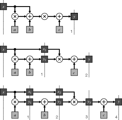
Pipelining may result in a small increase in logic block usage. This results from the need to introduce registers to construct the pipeline stages. These registers are implemented using flip-flops within the logic blocks. They are typically mapped onto unused flip-flops within the logic cells that are already used for implementing the logic. For example, the flip-flops to implement y1 will most likely be mapped to the flip-flops on the output of the logic cells implementing the adder. Register x1 does not correspond to any logic outputs, although it may be mapped to unused flip-flips of other logic within the design.
In the bottom panel of Figure 5.1 the pipeline is extended further, splitting the calculation over four clock cycles. This time, however, the clock period cannot be halved because the propagation delay of the multiplication is significantly longer than that of the adder. Stages 1 and 3 of the pipeline, containing the multipliers, will govern the maximum clock frequency. Consequently, although the maximum throughput can be increased a little, there is a larger increase in the latency because stages 2 and 4 have significant timing slack.
This imbalance in the propagation delay in different stages may be improved through retiming (Leiserson and Saxe, 1991). This requires some of the logic from the multiplication to be moved from stages 1 and 3 through registers y1 and y3 to stages 2 and 4, respectively. Depending on the logic that is shifted, and how it is shifted, there may be a significant increase in the number of flip-flops required as a result of retiming. Performing such fine-grained retiming manually can be tedious and error prone. Fortunately, retiming can be automated, for example it is provided as an optimisation option when compiling Handel-C designs (Mentor, 2010a). Retiming can even move the registers within the relatively deep logic created for multipliers and dividers; places that are not accessible within the source code. Such automated retiming can make debugging more difficult because it affects both the timing and the visibility of the intermediate signals.
If retiming is not available, or practical (for example where the output is fed back to the input of the same circuit for the next clock cycle), there are several techniques that can be used to reduce the logic depth (Mentor, 2010b). Of the arithmetic operations, division produces the deepest logic, followed by multiplication. Multiplication and division by constants (especially powers of two) can often be replaced by shifts or shifts and adds, while modulo operations based on powers of two can be replaced by simple bit selection. While long multiplication and division can be implemented efficiently with a loop, if a high throughput is required, the loop can be unrolled and pipelined (Bailey, 2006), with each loop iteration put in a separate pipeline stage. The ripple carry used for wide adders can increase the depth of the logic. Carry propagation can be pipelined by using narrower adders and propagating the carry on the next clock cycle. If carried to the extreme, this results in a form of carry save adder (see Parhami (2000) for some of the different adder structures). Greater than and less than comparisons are based on subtraction. If they can be replaced with equality comparisons, the logic depth can be reduced because the carry chain is no longer required.
Although a pipeline is a parallel computational structure in that each stage has separate hardware that operates in parallel with all of the other stages, from a dataflow perspective it is better to think of pipelines as sequential structures (Johnston et al., 2006b; 2010). Directly associated with the sequential processing is the pipeline latency. This is the time from when data is input until the corresponding output is produced. This view of latency is primarily a source-driven concept.
From a sink-driven perspective, the latency implies that data must be input to the pipeline at a predetermined time before the output is required. This period is referred to as priming the pipeline. If the output is synchronous, priming can be scheduled to begin a preset time before data is required at the output. Unfortunately, this is not an option when data is requested asynchronously by a sink. In this case, it is necessary to prime the pipeline with data and then stall the pipeline in a primed state until the data is requested at the output. This is discussed in more detail in the next section on synchronization. Source-driven processes may also be stalled if valid data is not available on every clock cycle.
During priming, the output is invalid, while the valid data propagates through the pipeline. The corresponding period at the end of processing is pipeline flushing, continuing the processing after the last valid data has been input until the corresponding data is output. Note that this use of the term pipeline flushing differs from that used with instruction pipelining of the fetch/decode/execute cycle; there flushing refers to the dumping of the existing, invalid, contents of the pipeline after a branch is taken, and repriming with valid data. The consequence of both priming and flushing is that the pipelined process must be clocked for more clock cycles than there are data elements.
5.1.2 Process Synchronisation
Whenever there are operations working in parallel, a recurring problem is the coordination of behaviour and communications between the different processes. This is relatively easy if all of the operations are streamed within a pipeline. However, it is more difficult for random access or hybrid processing modes, especially where the latencies may be different or where the time taken by the operations may vary. When there is a mix of processing modes, it is often necessary to synchronise the data transfer between operations.
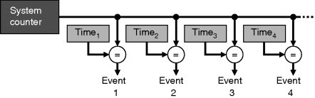
If all of the external events driving the system are regular and each operation has a constant processing time or latency, then global scheduling can be used. This can be accomplished by using a global counter to keep track of events and the algorithm state, as shown in Figure 5.2. The various operations are then scheduled by determining when each operation requires its data and matching the count. An example of global scheduling is processing an image on-the-fly as it is being displayed. Each line is the same length, with regular and synchronous events – the horizontal and vertical sync pulses. This enables the processing for each line to be scheduled to start so that the pipeline is primed when the data must be available for output to the display. Global scheduling requires all of the operations in the algorithm to be both predictable in their execution time, and tightly coupled.
Figure 5.2 Global scheduling derives synchronisation signals from a global counter.
Other communication and synchronisation methods must be used when each operation or module is loosely coupled. For source-driven processes, one way to achieve this is to associate a ‘data valid’ flag or token with the output. This token is then used to control the downstream operations or processes, by either stalling the process or continuing to run but ignoring the invalid data and marking the corresponding outputs as being invalid. For sink-driven applications, in addition to the data valid flag propagated downstream, it is also necessary to have a ‘wait’ flag or token propagated upstream (Mentor, 2010c). This is asserted when a processor is unable to accept further data on its input and requests the upstream process to stop providing data. Depending on the nature of each operation, it may be necessary to use FIFO buffers to smooth the flow of data between the processes. In particular, use of such buffers can simplify the management of pipeline priming and flushing. The interface between the operations within the PixelStreams library is based primarily on this form of synchronisation (Mentor, 2010c), and enables the operations to be kept separate and developed independently.
Another mechanism that allows point-to-point communication and synchronisation between concurrent processes is the CSP (communicating sequential processes) model (Hoare, 1985). One process is the transmitter, the other is the receiver, and they are connected by a data channel. Both processes must be ready before the communication or data transfer takes place. If one process is not ready, the other process will block or stall until both ends of the channel are ready. Thus, a CSP channel will ensure that both processes are synchronised at the point of data transfer. Channels can be used to pass data between operations in a pipeline, where they will automatically synchronise the processes. The fact that channels block when they are not ready allows them to be used with both source and sink driven pipelines. With source-driven flow, the downstream operations will stall when data is not available at the input. With sink-driven flow, the upstream operations will automatically prime and, then when the data is not read from the output, will stall waiting for the available data to be transferred. Note that because channels can block the execution of a process, care must be taken to avoid deadlocks caused by circular dependencies (Coffman et al., 1971).
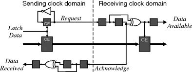
An example of channel synchronisation logic is shown in Figure 5.3. Identical logic is used to synchronise both the sender and receiver, so only the send logic will be described. If the receiver is not ready, then the Send signal is latched to remember that data is waiting to transfer. The Complete signal is clocked low to indicate that the sending process should wait. When the receiver becomes ready, the data will be transferred into the register on the next clock edge and the Complete signal is latched high for one clock cycle.
Figure 5.3 Channel synchronisation logic. (Adapted from Page and Luk, 1991.)

Combining the channel with a FIFO buffer will relax the timing constraints. It allows a source process to continue producing outputs until the FIFO buffer is full before it stalls. Similarly, a sink process will read available data from the FIFO buffer until the buffer is empty before it stalls.
The use of FIFO buffers enables operations with variable latency to be combined within a pipeline. In many video-based applications, where data is read from a camera or written to a display, the blanking intervals between rows and between frames can occupy a significant proportion of the total time. The strict timing of one pixel per clock cycle may be relaxed somewhat by enabling operations to work ahead during the blanking period, storing the results in a FIFO buffer, which can then be used to smooth out the timing bumps later.
5.1.3 Multiple Clock Domains
With some designs, using separate clocks and even different clock frequencies in different parts of a design are unavoidable. This is particularly the case when interfacing with external devices that provide their own clock. It makes sense to use the most natural clock frequency for each device or task, with different sections of the design running in separate clock domains. A problem then arises when communicating or passing data between clock domains, especially when the two clocks are independent, or when receiving asynchronous signals externally from the FPGA.
If the input of a flip-flop is changing when the flip-flop is clocked (violating the flip-flop's setup or hold times) the flip-flop can enter a metastable state where the output is neither a 0 nor a 1. When in this state, the output will eventually resolve to either a 0 or 1, but this can take an indeterminate time. Any logic connected to the output of the flip-flop will be affected, but because the resolution can take an arbitrarily long time, there is a danger that with the propagation delay through the logic, the setup times of downstream flip-flops may also be violated. The probability of staying in the metastable state decreases exponentially with time, so waiting for one clock cycle is usually sufficient to resolve the metastability. A synchroniser does just this; the output is fed to the input of a second flip-flop. The reliability of a synchroniser is expressed as the mean time between failures (Dike and Burton, 1999):
where ![]() is the settling time constant of the flip-flop, T is the period of the settling window allowed for metastability to resolve; the numerator gives the probability that any metastability will be resolved within the period T. TW is the effective width of the metastability window and is related to the setup and hold times of the flip-flop, fS is the frequency of the synchroniser's clock, and fT is the frequency of asynchronous data transitions on the clock domain boundary. The denominator of Equation 5.2 is the rate at which metastable transitions are generated. T is usually chosen so that the MTBF is at least ten times the expected life of the product (Ginosar, 2003). This is usually satisfied by setting T to be one clock period.
is the settling time constant of the flip-flop, T is the period of the settling window allowed for metastability to resolve; the numerator gives the probability that any metastability will be resolved within the period T. TW is the effective width of the metastability window and is related to the setup and hold times of the flip-flop, fS is the frequency of the synchroniser's clock, and fT is the frequency of asynchronous data transitions on the clock domain boundary. The denominator of Equation 5.2 is the rate at which metastable transitions are generated. T is usually chosen so that the MTBF is at least ten times the expected life of the product (Ginosar, 2003). This is usually satisfied by setting T to be one clock period.
To guarantee that data is transferred regardless of the relative clock frequencies of the transmitter and receiver, bidirectional synchronised handshaking is required (Ginosar, 2003). Such a circuit is shown in Figure 5.4. As the data is latched at the sending end, the Request line is toggled to indicate that new data is available. This Request signal is synchronised using two flip-flops. The resolution time is one clock period less the propagation delay of the exclusive OR gate and the setup time on the clock enable of the data latch. The exclusive OR gate detects the transition on the Request line, which is then used to enable the clock on the data latch (the data from the sending clock domain will have been stable for at least one clock cycle and does not require separate synchronisation), and provides a single pulse out on the Data Available line. An Acknowledge signal is sent back to the sending domain, where again it is synchronised and a Data Received pulse generated. It is only after this signal has been received that new data may be safely latched into the sending register. Otherwise, new data may overwrite the old in the sending data register before the contents have been latched at the receiver.
Figure 5.4 Bidirectional handshaking circuit for data synchronisation across clock domains.
This whole process can take either three or four clock cycles of the slowest clock domain, limiting the throughput to this rate. If the sending domain is always slower, then the acknowledgement logic may be saved by limiting the input to send every three clock cycles. The danger with this, though, is that if the clock rates are later changed, the synchronisation may no longer be valid (Ginosar, 2003).
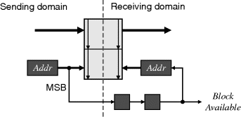
An alternative approach based on using dual-port fabric RAM as a form of FIFO buffer is shown in Figure 5.5. The RAM has one port in each clock domain and enables data to be queued while the synchronisation signal is sent from one domain to the other. This enables a sustained throughput of one data element per slow clock cycle. The most significant bit of the sending domain's address counter is sent across the domain boundary using a pair of synchronisation flip-flops to resolve metastability. This is then used to indicate when one block of data (half of the RAM) is available and the receiver can start to read. A small amount of logic prevents the address counter from addressing past the end of the available block. To provide safe transfer regardless of which clock domain is slower, both address counters should be interlinked to make access to the two halves of the address space mutually exclusive.
Figure 5.5 Transfer from a slower sending domain using a dual-port RAM.
5.2 Memory Bandwidth Constraints
Some operations require images to be partially or wholly buffered. While current high-capacity devices have sufficient on-chip memory to buffer a single image, in most applications it is poor use of this valuable resource to simply use it as an image buffer. For this reason, image frames and other large data sets are more usually stored in off-chip memory. This effectively places large amounts of data behind limited bandwidth and serialised (at the data word level) connections.
For this reason, it is essential to process as much of the data as possible while it passes through the FPGA, and to limit the data traffic between the FPGA and external devices. The standard software approach is to read each pixel required by an operation from memory, apply the operation and write the results back to memory. This is then repeated for every pixel within the image. A similar process is repeated for every operation that is applied to the image. The continual reading from and writing to memory may be avoided in many places by using a pipelined stream processing architecture.
Some operations cannot achieve this and may require an appropriate design of the memory architecture to overcome bandwidth problems. Other operations may be modified to cache data that is reused. For example, row buffering is a form of caching where pixel values read at one time are saved for reuse when processing subsequent rows.
5.2.1 Memory Architectures
The simplest way to increase memory bandwidth is to have multiple parallel memory systems. If each memory system has separate address and data connections to the FPGA, then each can be accessed independently and in parallel.
The crudest approach is to have multiple copies of the image in separate memory banks. Each bank can then be accessed independently to read the required data. For off-chip memory this is not the most memory efficient architecture, but it can be effective for on-chip caching when multiple processors require independent access to the same data.
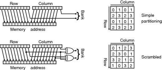
With many operations, it is likely that adjacent pixels need to be accessed simultaneously. By partitioning the address space over multiple banks, for example using one memory bank for odd addresses and one for even addresses, adjacent addresses may be accessed simultaneously. This can be applied to both the row and column addresses, so, for example, four banks could be used to access the four pixels within a 2 × 2 block (top panel of Figure 5.6). Rather than simply partitioning the memory, the addresses may be scrambled to enable a larger number of useful subsets to be accessed simultaneously (Lee, 1988; Kim and Kumar, 1989). For example, the bottom panel of Figure 5.6 enables four adjacent pixels in either a row or a column to be accessed simultaneously. It also allows the main diagonal and the anti-diagonal of a 4 × 4 block, and many (but not all) 2 × 2 blocks to be accessed concurrently (Kim and Kumar, 1989). It is not possible to have all 4 × 1, 1 × 4 and 2 × 2 blocks all simultaneously accessible with only four memory banks. This can be accomplished with five banks, although the address logic is considerably more complex as it requires division and modulo 5 remainders (Park, 1986). In addition to the partitioning and scrambling logic, a series of multiplexers is also required to route the address and data lines to the appropriate memory bank.
Figure 5.6 Memory partitioning schemes. Top: simple partitioning allows access of 2 × 2 blocks; bottom: scrambling the address allows row, column and main diagonal access.
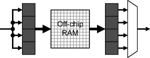
A further approach to increasing bandwidth is to increase the word width of the memory. Each memory access will then read or write several pixels. This is effectively connecting multiple banks in parallel but using a single set of address lines common to all banks. Additional circuitry, as shown in Figure 5.7, is usually required to pack the multiple pixels before writing to memory, and to unpack the pixels after reading, which can increase the propagation delay or latency of this scheme. Data packing is effective when pixels that are required simultaneously or on successive clock cycles are packed together. This will be the case when reading or writing streamed images.
Figure 5.7 Packing multiple pixels per memory location.
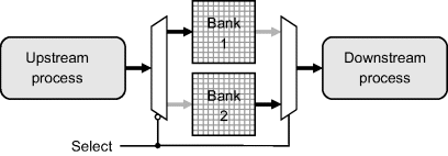
Another common use of multiple memory banks is bank switching or double buffering. Bank switching is used between two successive image processing operations to decouple the memory access patterns. This makes it useful when pipelining random access image processing operations, or with the hybrid processing mode to connect between stream processing and random access processing. It uses two coupled memory banks, as shown in Figure 5.8. The upstream process has access to one bank to write its results while the downstream process accesses data from within a second bank. When the frame is complete, the role of the two banks is reversed, making the data just loaded by the upstream process available to the downstream process. Bank switching therefore adds one frame period to the latency of the algorithm.
Figure 5.8 Bank switching or double buffering.
If the upstream and downstream processes have different frame rates, or are not completely synchronised, then the two processes will want to swap banks at different times. If the bank switching is forced by one process when the other is not ready, this can result in tearing artefacts, with part of the frame containing old data and part new. This problem may be overcome by triple buffering, using a third bank to completely separate the reading and the writing (Khan et al., 2009). This has the obvious implication of increasing the component count of the system and will use a larger number of I/O pins.
Bandwidth can also be increased by using multiport memory. Here the increase is gained by allowing two or more concurrent accesses to the same block of memory through separate address and data ports. While this is fine in principle, in practise it is not used with external memory systems because multiport memory is more specialised and consequently considerably more expensive.
A more practical approach to mimic multiport memory is to run the memory at a higher clock speed than the rest of the system. The resulting design will allow two or three accesses to memory within a single system clock period. The memory clock should be synchronised with the system clock to avoid synchronisation issues. Double data rate (DDR) memory is one example of memory that allows two data transfers per clock cycle, using both the falling and rising edges of the clock. A higher frequency RAM clock is only practical for systems with a relatively low clock speed, or with high speed memories.
Alternatively, the complete design could be run at the higher clock speed, with the data entering the processing pipeline every several clock cycles. Such approaches are called multiphase designs, with several clock cycles or phases associated with the pixel clock. Multiphase designs not only increase the bandwidth, but can also reduce computational hardware by reusing the hardware in different phases. The extreme is multiphase design is the Tabula ABAX FPGA, where the complete logic of the FPGA is changed in each of up to eight phases (Section 2.4.6).
5.2.1.1 Memory Technologies
It is generally best to use static memory for frame buffers, especially where they are accessed randomly and frequently. Static memory is faster than dynamic memory and is usually lower power. However, because it uses six transistors per bit rather than the one used by dynamic memory it is also more expensive. Many modern high speed static memories have been designed for use as instruction and data caches for high end serial computers. Consequently, they operate best in a burst mode and can take one or more clock cycles to switch between reading and writing (bus turnaround). Zero bus turnaround (ZBT) memories are designed with no dead period, enabling true low latency random access. This makes them easier to interface to an application, making them a good choice for frame buffers.
Dynamic memory is better for large volumes of data where there is not a strict time constraint. This is because dynamic memory is slower and generally requires several clock cycles latency from when the address is supplied to when the data is available. Dynamic memories have their highest bandwidth when operated in burst mode, with a series of reads or writes on the same row. They are also significantly harder to interface to for two reasons. They must be refreshed periodically (usually every 64 ms) by accessing every row once within this period. The internal structure means that when a row is accessed, all values on that row are available internally, with the column address selecting the entry on the row. Because of this segmented address structure, the row address is required before the column address. Usually, the row and column addresses share the same pins. All of these factors mean that some form of caching may be required to smooth the flow of data to or from the memory.
5.2.2 Caching
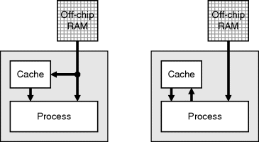
A cache memory is a small memory located close to a processor that holds data loaded from an external data source, or results that have been previously calculated. It provides rapidly accessible temporary storage for data that is used multiple times. The benefit of a cache is that it has faster access than re-reading the data from external memory (or hard disk) or recomputing the data from original values.
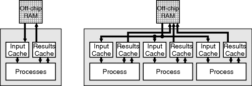
On an FPGA, a cache can be used to buffer accesses to external memory, particularly memory with a relatively long latency or access time, or operates in burst mode. In this capacity, it can also be used to smooth the flow of data between off-chip memory and the application. The cache can significantly reduce the bandwidth required between the FPGA and memory if the data in the cache is used multiple times (Weinhardt and Luk, 2001a). In some applications, the cache is positioned between the processor and the main memory, as shown in Figure 5.9, with accesses made to the cache rather than the memory. The cache controller in this case is then responsible for ensuring that the required data will be available in the cache. A separate cache is often used to hold the results to be written back to memory. With some operations, for example clustering or classifier training algorithms, the task may be accelerated by using multiple parallel processors working independently from the same data. Since the block RAMs on the FPGA can all be accessed independently, the cache bandwidth can be increased by having multiple separate copies of the cached data (Liu et al., 2008), one for each process. This allows each process to access the data without conflict with other processes. Whether there is a single results cache or multiple distributed results caches will depend primarily on how the results are reused by the processes. In Figure 5.9 it is assumed that results are only reused locally.
Figure 5.9 Caching as an interface to memory. Left: a single cache is shared between processes; right: data is duplicated in multiple input caches, but each process has a separate results cache.
One possible structure for the caches is an extended FIFO buffer. With a conventional FIFO buffer, only the item at the head of the buffer is available, and when it is read it is removed from the buffer. However, if the access and deletion operations are separated, and the addressing made external so that not just the head of the buffer is accessible, then the extended FIFO buffer can be used as a cache (Sedcole, 2006). With this arrangement, data is loaded into the buffer in logical blocks. Addressing is relative to the head of the buffer, allowing local logical addressing and data reuse. When the processing of a block is completed, the whole block is removed from the head of the FIFO buffer, giving the next block the focus.
Another arrangement is to have the cache in parallel with the external memory, as shown in Figure 5.10, rather than in series. This allows data to be read from the cache in parallel with the memory, increasing the bandwidth. The cache can be loaded either by copying the data as it is loaded from memory or by the process explicitly saving the data that it may require later into the cache.
Figure 5.10 Parallel caches.
5.2.3 Row Buffering
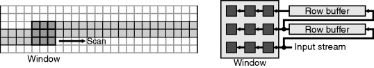
One common form of caching is row buffering. Consider a 3 × 3 window filter – each output sample is a function of the nine pixel values within the window. Without caching, nine pixels must be read for each window position (each clock cycle for stream processing) and each pixel must be read nine times as the window is scanned through the image. Pixels adjacent horizontally are required in successive clock cycles, so may be buffered and delayed in registers. This reduces the number of reads to three pixels every clock cycle. A row buffer caches the pixel values of previous rows to avoid having to read the pixel values in again (Figure 5.11). A 3 × 3 filter spans three rows, the current row and two previous rows; a new pixel is read in on the current row, so two row buffers are required to cache the pixel values of the previous two rows.
Figure 5.11 Row buffering caches the previous rows so they do not need to be read in again.
Each row buffer effectively delays the input by one row. An obvious implementation of such a digital delay would be to use an N-stage shift register, where N is the width of the image. There are several problems with such an implementation on an FPGA. Firstly, a shift register is made up of a chain of registers, where each bit uses a flip-flop. Each logic cell only has one flip-flop, so a row buffer would use a significant proportion of the FPGAs resources. Some FPGAs allow the logic cells to be configured as shift registers. This would use fewer of the available resources, since each cell could provide a delay of up to 16 (or 32 for the Virtex 5; Xilinx, 2008f) clock cycles.
A better use of resources would be to use a block RAM as a row buffer. Block RAMs cannot be directly configured as shift registers (one exception is Altera's Cyclone and Stratix devices), although most of the newer FPGAs can configure them as FIFO buffers, which can be arranged to provide an equivalent functionality. Those that natively provide FIFO buffers will automatically manage the addressing of the RAM. Otherwise, a FIFO buffer may be built from a dual-port memory, as shown in Figure 5.12. Two counters are needed, one for providing the address for writing to the memory and one for reading. The memory is used as a circular buffer, with the first address appearing sequentially after the last address within the memory. For blocks of memory that are a power of two long, this is achieved by allowing the address counters to wrap around. If the memory is other than a power of two long, then the counter has to be modified to reset to 0 after the last address is reached. A small amount of logic is also required to detect when the buffer is full or empty, although for use as a row buffer this is not necessary. The buffer is empty when the read and write addresses are identical, and full if incrementing the write address would make it equal to the read address.
Figure 5.12 Circular memory based FIFO buffer. The full and empty detection logic is not required for use as a row buffer.
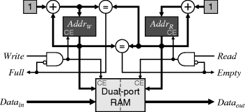
A FIFO buffer can be used as a shift register as follows. Assume that the buffer is initially empty. A series of N writes to the FIFO buffer will advance the write position to N locations ahead of the read position. Then, if a read and write are preformed simultaneously every clock cycle, the value read will be delayed from that written by N clock cycles. If the counters are provided explicitly, then resetting the read counter to 0 and the write counter to N would create an N-stage shift register. Since both counters are incremented at the same time, a single counter could be used, with an adder to offset it by N to get the write address. If the size of the RAM is exactly the same as the width of the image then the read address will always be the same as the write address, simplifying the circuit further.
Note that having multiple buffers in parallel, such as in Figure 5.11, is the same as a single buffer but with a wider data path. If implemented using separate RAM blocks, the address counters may be shared.
In many applications, it is necessary to maintain a column address, even if only for the purposes of reading from or writing to a frame buffer. This column address may be used to index the buffer rather than using a separate counter. The buffer is then no longer circular, but is automatically indexed to the current position in the image.
5.2.4 Other Memory Structures
With current technologies, memory is inherently a serial device. Although internally, data is stored in parallel, with a separate latch (or capacitor for dynamic memory) per bit stored. (While some more recent dynamic RAMs can store multiple bits per capacitor using different levels, this does not affect the argument here.) However, the addressing and access mechanisms mean that only one memory location can be selected for reading or writing at a time. Multiple data items can, therefore, only be accessed serially.
FIFO and circular buffers have been described in some detail in the previous section on row buffering. A FIFO buffer allows data items to be visited twice, the first time when the data items are loaded into the buffer, and the second time when they are retrieved.
Other useful memory structures are stacks, linked lists, trees and hash tables.
5.2.4.1 Stacks
Stacks also allow data items to be visited twice, although the second time the items are accessed in the reverse order. Items are pushed onto a stack by storing them in successive memory locations. When an item is popped from the stack, the most recently saved item is retrieved first. Stacks are, therefore, a form of first-in last-out or last-in first-out queue.
A stack can be implemented using a single-port memory, combined with a single address counter as the stack pointer, SP, as shown in Figure 5.13. It is usual for the stack pointer to address the next available free location. A push writes to the top of stack, as pointed to by SP and increments the stack pointer to point to the next free location. A pop needs to decrement the stack pointer before reading to access the data on the top of the stack.
Figure 5.13 Implementation of a stack.
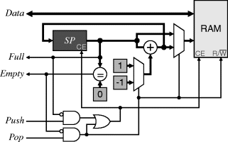
In the implementation shown above, a multiplexer is used to add either 1 or −1 to SP depending on whether a Push or Pop operation is used respectively. A Push uses SP directly as the RAM address, whereas a Pop uses the decremented SP as the address. The stack is empty if the address is zero; in this condition, a Pop is not allowed because there is nothing left on the stack to pop. Note that the test for zero can be implemented by simply taking the NOR of all of the bits. The stack is full after the last memory element is written. Incrementing SP will wrap it past the end. This is prevented by making SP one bit longer than needed to address the memory. The stack is then full when the most significant bit of SP is set.
5.2.4.2 Linked Lists
A linked list is useful for maintaining a dynamic collection of data items. Each item is stored in a separate location in the memory; however, successive items are not necessarily in sequential memory locations. Associated with each item is a pointer to the next item (a pointer to an item is just the memory address of that item), resulting in an implicit ordering of the items within the list. Linked lists have an advantage over arrays when inserting an item into the list. To insert an item into an array, all the successive items in the array must be moved to new memory locations to make space at the appropriate position in the array. However, with a linked list, the new item can be stored in any free memory location and the pointers adjusted to put it into the correct place in the sequence. Similarly, when deleting an item from an array, all subsequent items must be shifted back. With a list it is only necessary to adjust the pointers to skip the item that is removed.
The first item in the list is called the head of the list. The last item in the list has a null pointer, ∅, indicating that there is no next item. On software systems, 0 is often used as the null pointer because 0 is not usually a valid data address. However, on FPGAs 0 usually is a valid data address. This may be resolved either by using a separate flag to indicate a null pointer, or by not using location 0 to hold data. The former approach requires one extra bit per pointer to contain the null pointer flag but it does mean that only one bit needs to be tested to determine if it is a null pointer. Not using location 0 reduces the number of items that may be stored in a block of memory by one item and a null pointer can be tested by checking if all bits are 0.
One problem with linked lists is keeping track of which memory locations are free. There are two approaches to solving this problem. One is to maintain a series of one bit registers indicating that a memory location is free. Associated with this is a priority encoder to translate the first 1 into the corresponding address. While this is suitable for short lists, it can quickly get expensive as the address space gets larger. A second approach is to reuse the linking mechanism to maintain a second list of unused entries. This requires that the memory be initialised with the links before being used.
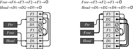
Inserting new data into a list requires four memory accesses (Figure 5.14). Assume that it is necessary to insert the new data item, D4, after D2 and that there is currently a pointer to D2. Also assume that unused entries are in a list pointed to by Free. The first access is to read the pointer associated with D2 (the pointer to D3). The pointer is then changed to point to the head of the free list (which will become the new data item), and is written back to D2. The item pointed to by the head of the free list (the pointer associated with F4) becomes the new head, so it must be read from the memory. Finally, the new data and pointer to D3 is written to the new element.
Figure 5.14 Inserting an element into a linked list. Changed links are shown in bold.
To implement even this relatively simple operation on an FPGA would require a finite state machine to sequence each of the steps. The controlling state machine would require a series of branches to manage each different operation: initialisation, traversing a list, insertion and deletion. Since each operation will require several clock cycles, it will be necessary to include synchronisation logic between the linked list and the rest of the design.
Note that the sequential ordering means it is necessary to insert an item either after a specified item in the list or at the head of the list. Items cannot be directly inserted before a specified item because there is no direct reference to the previous item in a list. The previous item points to the specified item; to insert an entry this pointer needs to be changed to point to the new item. With a singly linked list, the only way to locate the previous item is to sequentially scan through the list from the head.
This limitation can be overcome by using a doubly linked list; this has bidirectional links, to both the previous and the next items in the list. Having the extra link also means that extra memory accesses are required when inserting and deleting links. The extra pointer associated with each data item would also require a wider memory.
5.2.4.3 Trees
Another data structure commonly used in computer vision to represent hierarchically structured data is a tree. An example tree is shown on the left in Figure 5.15. The node at the top of the tree is called the root node; node A is the root in this example. The nodes immediately below a node are called the child nodes. For example, D, E and F are children of B, and B is their parent. Nodes that have no children are leaf nodes. In this example, D, F, G, I, J and K are the leaf nodes.
Figure 5.15 A representation of a tree.
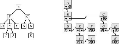
In a general tree, a node can have an arbitrary number of children. Therefore, it is inconvenient for a node to point to all of its children. One general representation of a tree is as a form of two-dimensional linked list. Every node has two pointers: one to its first child (or null if it is a leaf node) and one to its next sibling. In this way, all of the children of a node are contained in a linked list. This approach to representing a tree is shown in Figure 5.15.
Note that this method is suitable for navigating from the root of a tree down to a node, but there is no pointer from a child to its parent so navigating back up the tree is more difficult. This may be overcome by using doubly linked lists, but would require every node to maintain three pointers. A more efficient alternative in many applications is to use a separate memory structure to remember the context of a node. When performing a depth-first traversal of the tree, a stack can be used to remember parent nodes. As the link from a node to its first child is taken, a pointer to the node can be pushed onto a stack. Then to move back up the tree after reaching a leaf, it is only necessary to pop the most recently visited parent from the stack. The stack therefore provides the required link from a child back to its parent. If performing a breadth-first search, it is more appropriate to use a FIFO queue. As a node is visited, if it has any children the pointer to the first child node is stored in the queue. Then when the last child is reached, the first entry in the queue is the next node to visit.
One particular type of tree deserves special mention is a binary tree. It has at most two children, so for a binary tree it is possible to (and indeed useful to) directly point to the two children rather than having a list to represent the children.
5.2.4.4 Hash Tables
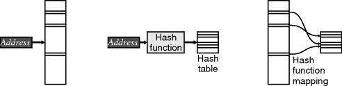
A sparse array is an array with a large address space, but only a small proportion of the array has data at any one time. If the whole array is reserved, this can be wasteful of the memory resources available on an FPGA. While the memory requirement of the array may be significantly reduced using a linked list or tree to represent the occupied data elements, these structures incur a significant overhead of having to search through the list or tree to find a particular element.
An alternative approach is to store the data using a hash table. As shown in Figure 5.16, the original address is mapped using a hash function to a much smaller address space, that of the hash table, where the data is actually stored. The reduction memory comes at the cost of evaluating the hash function. In most applications, this cost can be lower than that of searching through a linked list or tree.
Figure 5.16 Address hashing. Left: original sparse address space; centre: using a hash function to reduce address space; right: the mapping between address spaces by the hash function.
A good hash function is one that maps the different input addresses that are actually used to different slots within the hash table. If the input addresses can be considered random, then a simple and effective hash function can be to use a subset of the bits of the input address. However, if the set of input addresses is likely to be clustered, then a good hash function will distribute these to quite different slots to reduce the chance that multiple input addresses will map to the same slot. For this reason, a common technique is to base the hash function on a pseudorandom number generator, using the input address as the seed. This will tend to map the input addresses randomly throughout the hash table.
Inevitably, though, there will be address collisions, with multiple input addresses mapping to a common slots. There are two main approaches for resolving such collisions. One is to store multiple elements per slot, using a linked list for example. This requires additional data structures to the hash table. Another alternative is to use a so-called open addressing scheme to store the data in the next available slot (Peterson, 1957). Both methods require a search in the event of collisions. The search is kept small by ensuring that the used slots are randomly distributed and the hash table is not too full. Open addressing is sensitive to the fill factor of the hash table (the proportion of slots that are used) and it is generally better to keep the maximum fill factor below about 75%. There are several advanced techniques (Askitis, 2009) that can be used to increase the fill factor, but these generally come at the expense of more complex hash functions.
A hash table can be considered as a form of associative memory. The sparse addressing of hash tables makes them appropriate for implementing caches. When a hash table is used for a cache, whenever a collision occurs the previous entry can be discarded, avoiding the need for searching.
The input addresses do not necessarily need to be memory locations, but could be strings or other complex data structures that are reduced using the hash function to provide an index into the hash table.
The finite number of available resources in the system such as function blocks or local and off-chip RAM imposes a constraint. On an FPGA, there may be a number of concurrent processes that need access to a particular resource in a given clock cycle, which can result in contention, or undefined behaviour if both are permitted access.
5.3.1 Resource Multiplexing
An expensive resource may be shared between multiple parts of a design by using a multiplexer. There are three conditions required for this to be practical. Firstly, the cost of the resource must be less than the cost of the multiplexers required to share the resource. For example, sharing an adder in most instances is not practical because the cost of building a separate adder will usually be less that the cost of the multiplexers required to share the adder. However, sharing a complex functional block may well be practical. The second condition is that the resource must only be partially used in each of the locations that it is used. If the instances of the resource are fully used, then sharing a single instance between the multiple locations will slow the system down. The third consideration is the timing of when the resource is required. If the resource must be used simultaneously in multiple parts of the design, then multiple copies must be used.
The limitation of sharing a resource is that multiple simultaneous accesses to the resource are prohibited. Sharing often requires associating some form of arbitration logic with the resource to manage the access; some of the options for this are explored in more detail in the next section.
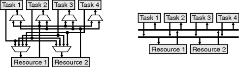
An option when only a few instances of a resource are required simultaneously with instances required by many tasks is to have a pool of resources. This approach is illustrated in Figure 5.17. When the resource pool is shared by a large number of tasks, the multiplexing requirements can become prohibitive. An alternative is to connect to the resources via busses. Note that the busses are additional resources that must also be shared, because only one task or resource may use a bus at a time.
Figure 5.17 Sharing a pool of resources amongst several tasks. Left: using multiplexers; right: using busses.
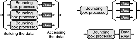
Sometimes, careful analysis of a problem can identify potential for resource sharing where it may not be immediately obvious. Consider obtaining the bounding boxes of a set of objects from a streamed input image consisting of labelled pixels, where the label indicates the associated object (see also Section 11.1). Since each object can appear anywhere in the image, and the bounding boxes for different objects may overlap, it is necessary to build the bounding boxes for each label in parallel. The computational structure for performing this is shown on the left in Figure 5.18. This has a separate processor for each label, building the bounding box for that label. A multiplexer is required on the output to access the data for a particular label for downstream processing. Careful analysis reveals that it is not the processor that needs to be separate for each label, because any given pixel input will have only one label, but rather it is the data that must be maintained separately for each label. Only a single bounding box processor is needed and this may be multiplexed between the different labels. Equivalently, the data registers for each label need to be multiplexed for the single instance of the bounding box processor. Multiplexing more than a few data registers can get quite expensive. Where the memory bandwidth allows, an efficient alternative is to use a RAM rather than registers because the RAM addressing effectively provides the multiplexing for free.
Figure 5.18 Sharing data with a resource. Left: processing each label with a separate bounding box processor; right: sharing a single processor but with separate data registers, which can be efficiently implemented using a RAM.
5.3.1.1 Busses
The example in Figure 5.17 highlights one of the problems with using multiplexers to connect multiple outputs to multiple inputs. Each input requires a multiplexer, with the width of the multiplexer dependent on the number of outputs connected. The complexity is therefore proportional to the product of the number of inputs and the number of outputs. This does not scale well as a new input or output is added.
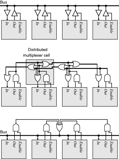
Such growth in complexity may be overcome by using a bus as shown in the top of Figure 5.19. With a bus, all of the inputs are connected directly to the bus, while the outputs are connected via a tri-state buffer. Enabling an output connects it to the bus, while disabling it disconnects it. The logic scales well, with each new device requiring only a tri-state buffer to connect.
Figure 5.19 Bus structures. Top: connecting to the bus with tri-state buffers; middle: implementing a bus as a distributed multiplexer; bottom: implementing a bus as a shared multiplexer. (Sedcole, 2006; reproduced by permission of P. Sedcole.)
This reduction in logic does not come without a cost. Firstly, with multiplexers, each connection is independent of the others. A bus, however, is shared amongst all of the devices connected to it. While a bus does allow any output to be connected to any input (in fact it connects to all of the inputs), only one output may be connected at a time. If multiple outputs attempt to connect simultaneously to the bus, this could potentially damage the FPGA (if the outputs were in opposite states). Therefore, an additional hidden cost is the arbitration logic required to control access to the bus.
Unfortunately, not many FPGAs have an internal bus structure with the associated tri-state buffers. An equivalent functionality may be constructed using the FPGAs logic resources (Sedcole, 2006), as shown in the middle of Figure 5.19. The bus is replaced by two signals, one propagating to the right and the other to the left. An enabled output from a device is ORed onto both signals, to connect it to devices in both directions. An input is taken as the OR of both signals. Such an arrangement is effectively a distributed multiplexer; if the expression on the input is expanded, it is simply the OR of the enabled outputs. If multiple outputs are enabled, the signal on all of the inputs may not be what was intended, but it will not damage the FPGA.
The disadvantage of the distributed multiplexer is that it requires the devices to be in a particular physical order on the FPGA. This was not a problem where it was initially proposed – for connecting dynamically reconfigurable functional blocks to a design (Sedcole, 2006). There the logic for each block connecting to the ‘bus’ was constrained to a particular region of the FPGA. For general use, a bus may be simply constructed using a shared multiplexer, as shown in the bottom of Figure 5.19.
When a bus is used to communicate between processes, it may be necessary for each process to have a FIFO buffer on its both its input and output (Sedcole, 2006). Appropriately sized buffers reduce the time lost when stalled waiting for the bus. This becomes particularly important with high bus use to cope with time varying demand while maintaining the required average throughput for each process.
5.3.2 Resource Controllers
There are potential resource conflicts whenever a resource is shared between several concurrent blocks. Any task that requires exclusive access to the resource can cause a conflict. Some common examples are:
- Writing to a register: Only one block may write to a register in any clock cycle. The output of the register, though, is available to multiple blocks simultaneously.
- Accessing memory, whether reading or writing: A multiport memory may only have one access per port. The different ports may write to different memory locations, writing to the same location from multiple ports will result in undefined behaviour.
- Sending data to a shared function block for processing: Note that if the block is pipelined, it may be processing several items of data simultaneously, each at different stages within the pipeline.
- Writing to a bus: While a bus may be used to connect to another resource, the bus is a resource in its own right, since only one output may write to the bus at a time.
Since the conflicts may occur between quite different parts of the design that may be executing independently, none of these conflicts can be detected by a compiler. The compiler can only detect potential conflicts through the resource being connected in multiple places and, as a result, it builds the multiplexer needed to connect to the shared resource. The conflicts are run-time events; therefore, they must be detected and resolved as they occur.
A good design principle is to reduce the coupling as much as possible between parallel sections of an algorithm. This will tend to reduce the number of unnecessary conflicts. However, some coupling between sections is inevitable, especially where expensive resources are shared.
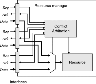
One way of systematically managing the potential conflicts is to encapsulate the resource with a resource manager (Vanmeerbeeck et al., 2001) and access the resource via a set of predefined interfaces, as shown in Figure 5.20. If necessary, the interface should include handshaking signals to indicate that a request to access the resource is granted. Combining the resource with its manager in this way makes the design easier to maintain, as it is only the manager process that interacts directly with the resource. It also makes it easier to change the conflict resolution strategy because it is in one place, rather than distributed throughout the code wherever the resource is accessed.
Figure 5.20 Encapsulating a resource with a resource manager simplifies the design.
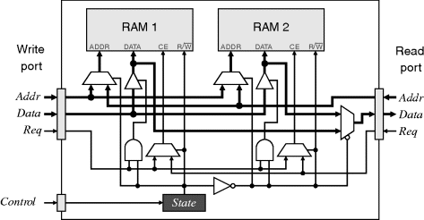
For example, Figure 5.21 shows a possible implementation of the double-buffered bank switching introduced in Figure 5.8. In this example, the conflict resolution mechanism is scheduled separate access, so no handshaking is required. The State variable controls which RAM bank is being written to and which is being read from at any one time. The specific banks are hidden from the tasks performing the access. The upstream task just writes to the write port as though it was ordinary memory, and the resource controller directs the request to the appropriate RAM bank. Similarly, when the downstream task reads from the buffer, it is directed to the other bank. The main difference between access via the controller and direct access to a dedicated RAM bank is the slight increase in propagation delay through the multiplexers.
Figure 5.21 Resource manager for bank switched memories.
A CSP model (Hoare, 1985) is another approach for managing the communication between the resource controller and the processes that require access to the resource. This effectively uses a channel for each read and write port, with the process blocking until the communication can take place. The blocking is achieved in hardware by using a handshake signal to indicate that the data has been transferred.
5.3.2.1 Conflict Arbitration
A conflict occurs when multiple processes attempt to access a resource at the same time. If there is no conflict resolution in place, the default will be for all of the processes to access the resource simultaneously. The multiplexers used to share the resource will prevent any physical damage to the FPGA (although care needs to be taken with busses). However, the multiple selections will be combined in a manner that depends on the multiplexer design (Figure 4.7). Generally, this will have undesired results and could be a cause of bugs within the algorithm that could be difficult to locate.
With conflict resolution, only one process will be granted access to the resource and the other processes will be denied access. These processes must wait for the resource to become free before continuing. While it may be possible to perform some other task while waiting, this can be hard to implement in practise. In some circumstances, it may be possible to queue the access (for example using a FIFO buffer) and continue if processing time is critical. It is more usual, however, simply to stall or block the process until the resource becomes free.
The simplest form of conflict resolution is scheduled access. With this, conflict is avoided by designing the algorithm such that the accesses are separated or scheduled to occur at different times. In the bank-switch example above, accesses to each bank of RAM are separated in time. While data is being stored in one bank, it is being consumed from the other. At the end of the frame, the control signal is toggled to switch the roles of the banks. When stream processing is used, a shared resource may be available to other processes during the horizontal or vertical blanking periods. If multiple processes need to use the resource, simple synchronisation mechanisms may be used to pass access from one process to the next.
Scheduled access can also be employed at a fine grain by using a multiphase pipeline. Consider normalising the colour components of YCbCr data (Johnston et al., 2005b) (on the left in Figure 5.22): each of Cb and Cr are divided by Y to normalise for intensity as part of a stream processing pipeline:
(5.3) ![]()
Figure 5.22 Sharing a divider in a two-phase pipeline.
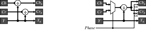
The divider is a relatively expensive resource, so sharing its access may be desirable. Since the pixel clock is often slow compared with the capabilities of modern FPGAs, the clock frequency can be doubled, creating a two-phase pipeline. New data is then presented at the input (and is available at the output) on every second clock cycle. However, with two clock cycles available to process every pixel, the divider (and other resources) can now be shared, as shown on the right in Figure 5.22. In one phase, Cb is divided by Y and stored in Cbn, and in the other phase Cr is similarly processed. If necessary, the divider can be pipelined to meet the tighter timing constraints, since each of Cb and Cr are being processed in separate clock cycles. It is only necessary to use the appropriate phase of clock to latch the results into the corresponding output register.
When the processes are able to be synchronised, scheduled access works well and is easy to implement. However, scheduling requires knowing in advance when the accesses will occur. It is difficult to schedule asynchronous accesses (asynchronous in the sense that they can occur in any clock cycle; the underlying resources must be in one clock domain so are still driven by a common clock).
With asynchronous accesses, it is necessary to build hardware to resolve the conflict. The type of hardware required depends on the duration of the access. If the duration is only a single clock cycle, then relatively simple conflict resolution such as a simple prioritised acknowledgement (left panel of Figure 5.23) may be used. With a prioritised access, different parts of the algorithm have different priority with respect to accessing a resource. The highest priority section is guaranteed access, while a lower priority section can only gain access if the resource is not being used by a higher priority section. That is:
Figure 5.23 Priority-based conflict resolution. Left: a simple prioritised acknowledgement; right: a prioritised multiplexer.
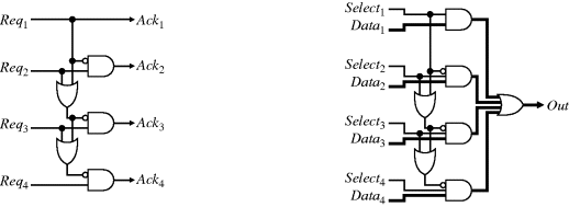
where a smaller subscript corresponds to a higher priority. The implementation shown in Figure 5.23 is suitable for providing a clock enable signal for a register or some other circuit where the output is sampled on the clock. This is because the propagation delays of the circuit generating the Req signals mean that there can be hazards on the Ack outputs. If such hazards must be avoided, then the Ack outputs can be registered, delaying the acknowledgement until the following clock cycle.
One example of a prioritised access is the prioritised multiplexer shown in the right panel of Figure 5.23. The output will correspond to the highest priority selected input. This could be used, for example, in selecting the pixel to display. Only one pixel may be displayed at any location and a standard multiplexer would combine the pixel values if multiple inputs were selected. By assigning each source a priority, only a single value will be selected. This effectively creates a series of layers or overlays on the display, with the background (lower priority) layers only being visible when a foreground layer is not selected.
Another example of prioritised access is lookahead caching. Consider a streamed operation that requires zero, one or two accesses to memory in a clock cycle depending on the local context. Also assume that the average number of memory accesses per clock cycle is less than or equal to one. The operation may be split into two processes: one that produces the streamed output at one pixel per clock cycle, and one that looks ahead to where two accesses are required and preloads one of those values into a cache. The output process will have the higher priority for memory access because it must produce its streamed output on time. The cache process, however, can access memory whenever the output process does not require it.
If the conflict duration is for many clock cycles, then a semaphore is required to lock out other tasks while one task has access. Equation 5.4 then becomes:
(5.5) ![]()
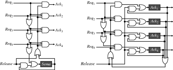
where the first two terms determine the prioritised input as before. The third term selects the prioritised input if either the semaphore, Sema, is not set or when the semaphore is released. In the latter case, the highest priority waiting task is then acknowledged. Sema is effectively a flag that indicates whether a resource is currently being used (on the left in Figure 5.24). Any request will set the semaphore, which will remain set until released. The new value of the semaphore, Sema′, is:
(5.6) ![]()
Figure 5.24 A prioritised semaphore. Left: a single semaphore flag; right: a separate flag for each task, to indicate which task currently has the semaphore.
When a request is acknowledged, the semaphore is set, which prevents further requests from being acknowledged. Note that this also means that the Ack output only goes high for one clock cycle to acknowledge the request. Again, with this circuit there may be hazards on the Ack outputs, which may be removed if necessary by adding a register on each output.
If it is necessary to know which task has the semaphore, one method is to hold the corresponding Ack output high while that task has access. This requires a separate flag for each task, as shown on the right in Figure 5.24, where each flag is set by:
(5.7) ![]()
This works on the same principle as before, with any of the semaphores blocking the requests until the Release input is asserted. With this circuit, once a lower priority task gains the semaphore, it will block a high priority task. If necessary, it may be modified further to enable a high priority task to pre-empt a lower priority task:
(5.8) ![]()
Care must be taken when using semaphores to prevent deadlock. A deadlock may occur when the following four conditions are all true (Coffman et al., 1971):
- Tasks claim exclusive control of the resources they require.
- Tasks hold resources already allocated while waiting for additional resources.
- Resources cannot be forcibly removed by other tasks. They must be released by tasks using the resource.
- There is a circular chain of tasks, where each task holds resources that are being requested by another task.
Deadlock may be prevented by ensuring that any one of these conditions is false. For complex systems, this is perhaps easiest achieved by requiring tasks to request all of the resources they require simultaneously. If not all of the resources are available, then none of the resources are allocated. This requires modification of semaphore circuit to couple the requests. It still does not necessarily avoid deadlocks unless care is taken with the priority ordering. For example, consider two tasks that both require the same two resources simultaneously. If the priority order is different for the two resources, then, because of the prioritisation, each task will prevent the other from gaining one of the resources, resulting in a deadlock.
5.3.3 Reconfigurability
In most applications, a single configuration is loaded onto the FPGA prior to executing the application. This configuration is retained, unchanged, until the application is completed. Such systems are called compile-time reconfigurable, because the functionality of the entire system is determined at compile time and remains unchanged for the duration of the application (Hadley and Hutchings, 1995).
Sometimes, however, there are insufficient resources on the FPGA to hold all of a design. Since the FPGA is programmable, the hardware can be reprogrammed or reconfigured dynamically, while still executing an application. Such systems are termed run-time reconfigurable (Hadley and Hutchings, 1995). This requires the algorithm to be split into multiple sequential sections, where the only link between the sections is the partially processed data. Since the configuration data for an FPGA includes the initial values of any registers and the contents of on-chip memory, any data that must be maintained from the old configuration to the new must be stored off-chip (Villasenor et al., 1996) to prevent it from being overwritten. Unfortunately, reconfiguring the entire FPGA can take a significant time– large FPGAs typically have reconfiguration times of tens to hundreds of milliseconds. This latency must be taken into account in any application. With smaller FPGAs, the reconfiguration time may be acceptable (Villasenor et al.,;). The latency is usually less important when switching from one application to another, for example between an application used for tuning the image processing algorithm parameters and the application that runs the actual algorithm.
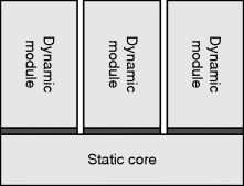
The time required to reconfigure the whole FPGA has spurred research into partially reconfigurable systems, where only a part of the FPGA is reprogrammed. Partial reconfiguration has two advantages over reconfiguring the entire FPGA. The first is that the configuration data for part of the FPGA is smaller than that for the whole chip, so will usually take significantly less time to load than a complete configuration file. It also has the advantage that the rest of a design can continue to operate while part of the design is being reconfigured. Not all FPGAs are partially reconfigurable; the bitstream must be able to split into a series of frames, with each frame including an address that specifies its target location within the FPGA. At present only some of the devices with the Xilinx range and the older Atmel AT40K support partial reconfiguration.
Partial reconfiguration requires a modular design, as shown in Figure 5.25, with a static core and a set of dynamic modules (Mesquita et al., 2003). The static core usually deals with interface and control functions and holds the partial results, while the reconfigurable modules typically provide the computation. The dynamic modules can be loaded or changed as necessary at run-time, a little like overlays or dynamic link libraries in a software system (Horta et al., 2002). Only the portion of the FPGA being loaded needs to be stopped during reconfiguration; the rest of the design can continue executing.
Figure 5.25 Designing for partial reconfigurability. A set of dynamic modules ‘plug in’ to the static core.
Between the dynamic modules and the static core, a standard interface must be designed to enable each dynamic module to communicate with the core or with other modules (Sedcole, 2006). Common communication mechanisms are to use a shared bus (Hagemeyer et al., 2007) or predefined pipeline ports connecting from one module to the next (Sedcole et al., 2003). Both need to be in standard locations to enable them to connect correctly when the module is loaded.
Two types of partial reconfiguration have been considered in the literature. One restricts the reconfigurable modules to being a fixed size that can be mapped to a small number of predefined locations. The other allows modules to be of variable size and be placed more flexibly within the reconfigurable region. The more flexible placement introduces two problems. Firstly, the heterogeneity of resources restricts possible locations that a dynamic module may be loaded on the FPGA. The control algorithm must not only search for a space sufficiently large to hold a module, but the space must also have the required resources in the right place. Secondly, with the loading and unloading of modules, it is possible for the free space to become fragmented. To overcome this, it is necessary to make the modules dynamically relocatable (Koester et al., 2007). To relocate a module (Dumitriu et al., 2009) it must first be stopped or stalled, then disconnected from the core. The current state (registers and memory) must be read back from the FPGA, before writing the module (including its state) to a new location, where it is reconnected to the core, and restarted.
Partial reconfigurability allows adaptive algorithms. Consider an intelligent surveillance camera tracking vehicles on a busy road. The lighting and conditions in the scene can vary significantly with time, requiring different algorithms for optimal operation (Sedcole et al., 2007). These different subalgorithms may be designed and implemented as modules. By having the part of the algorithm that monitors the conditions in the static core, it can select the most appropriate modules and load them into the FPGA based on the context.
Simmler et al. (2000) have taken this one step further. Rather than consider switching between tasks that are part of the same application, they propose switching between tasks associated with different applications running on the FPGA. Multitasking requires suspending one task and resuming a previously suspended task. The state of a task is represented by the contents of the registers and memory contained within the FPGA (or dynamic module in the case of partial reconfigurability). Therefore, the configuration must be read back from the FPGA to record the state or context. To accurately record the state, the task must be suspended while reading the configuration and while reloading it. However, not all FPGAs support readback, and therefore not all will support dynamic task switching.
At present, the tools to support partial dynamic configuration are quite low level. Each module must be developed with quite tight placement constraints to keep the module within a restricted region and to ensure that the communication interfaces are in defined locations. The system core also requires similar placement constraints to keep out of the reconfigurable region and to fix the communication interfaces. Xilinx provides an internal configuration access port (ICAP) to enable an embedded CPU to dynamically reconfigure part of the FPGA (Blodget et al., 2003). This can also be accessed directly by logic for partial reconfiguration without requiring a CPU (Lai and Diessel, 2009).
Regardless of whether full or partial reconfigurability is used, run-time reconfigurability can be used to extend the resources available on the FPGA. This can allow a smaller FPGA to be used for the application, reducing both the cost and power requirements.
An FPGA implementation is amenable to a wider range of computational techniques than a software implementation. Some of the computational considerations and techniques are reviewed in this section.
5.4.1 Number Systems
In any image processing computation, the numerical values of the pixels, coordinates, features and other numerical data must be represented and manipulated. There is a wide range of number systems that can be used. A full discussion of the range of number systems and associated logic circuits for performing basic arithmetic operations is beyond the scope of this book. The interested reader should refer to one of the many good books available on computer arithmetic (for example Parhami, 2000).
Arguably, the most common representation is based on binary or base-two numbers. As shown in Figure 5.26, a positive binary integer, B, is represented by a set of N binary digits, bi, where each digit represents a successive power of two. The numerical value of the number is then:
(5.9) ![]()
Figure 5.26 Binary number representation.
In most software representations, N is fixed by the underlying computer architecture at 8, 16, 32, or 64. On an FPGA, however, there is no necessity to constrain the representation to these widths. In fact, the hardware requirements can often be significantly reduced by tailoring the width of the numbers to the range of values that need to be represented (Constantinides et al., 2001). For example, for a 640 × 480 image the row and column coordinates can be represented by 9-bit and 10-bit integers respectively.
When representing signed integers, there are three common methods. The first is the sign-magnitude representation. This uses a sign bit to indicate whether the number is positive or negative, and the remaining N − 1 bits to represent the magnitude (absolute value) of the number. With this representation, addition and subtraction are slightly complicated because the actual operation performed will depend on the combination of sign bits and the relative magnitudes of the numbers. Multiplication and division are simpler, as the sign and magnitude bits can be operated on separately. The range of numbers represented is from ![]() to
to ![]() . Note that there are two representations for zero: −0 and +0.
. Note that there are two representations for zero: −0 and +0.
The two's complement representation is the format most commonly used by computers. Numbers in the range ![]() are represented modulo 2N, which maps the negative numbers into the range
are represented modulo 2N, which maps the negative numbers into the range ![]() . This is equivalent to giving the most significant bit a negative weight:
. This is equivalent to giving the most significant bit a negative weight:
(5.10) ![]()
Therefore, negative numbers can be identified by a 1 in the most significant bit. Addition and subtraction of two's complement numbers is exactly the same as for unsigned numbers, which is why the two's complement representation is so attractive. Multiplication is a little more complex; it has to take into account that the most significant bit is negative.
The third representation is offset binary, where an offset or bias is added to all of the numbers:
(5.11) ![]()
where Offset is usually (but not always) ![]() . Offset binary is commonly used in image processing to display negative pixel values. It is not possible to display negative intensities, so offsetting zero to mid-grey shows negative values as darker and positive values as lighter. Offset binary is also frequently used with A/D converters to enable them to handle negative voltages. Most A/D converters are unipolar and will only convert positive voltages (or currents). By adding a bias to a bipolar signal, negative voltages can be made positive enabling them to be successfully converted. A limitation with offset binary is that the offset needs to be taken into account when performing any arithmetic.
. Offset binary is commonly used in image processing to display negative pixel values. It is not possible to display negative intensities, so offsetting zero to mid-grey shows negative values as darker and positive values as lighter. Offset binary is also frequently used with A/D converters to enable them to handle negative voltages. Most A/D converters are unipolar and will only convert positive voltages (or currents). By adding a bias to a bipolar signal, negative voltages can be made positive enabling them to be successfully converted. A limitation with offset binary is that the offset needs to be taken into account when performing any arithmetic.
5.4.1.1 Real Numbers
One limitation of integer representations is their inability to represent real numbers. This may be overcome by scaling the integer by a fraction, so that the integer represents the number of fractions. If the fraction is made a negative power of two, for example ![]() , then the result is fixed-point notation. The resulting number is then:
, then the result is fixed-point notation. The resulting number is then:
(5.12) ![]()
where the integer B can be either unsigned or signed (usually two's complement). A convenient shorthand notation for the format of a fixed-point number is UN. k or SN. k, where the letter is either U or S to indicate an unsigned or signed N-bit integer is used with k fraction bits. As seen in Figure 5.27, the N-bit integer representation of the fixed-point number corresponds to shifting it k bits to the left.
Figure 5.27 Fixed-point number representation with resolution 2−3. Shifting the number 3 bits to the left gives the corresponding integer representation. This number is of type U8.3 or S8.3 depending on whether the weight of the most significant bit was positive or negative respectively.
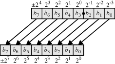
Most real numbers can only be represented approximately with a fixed-point representation. While increasing the number of bits to the right of the binary point will increase the accuracy of the approximation, many even relatively simple numbers cannot be represented exactly with a finite number of bits. For example, the fraction 1/3 has an infinitely repeating binary representation, 0.01010101010101 . . ., so any fixed-point (or even floating-point) representation will only ever be an approximation. The absolute error of the representation, or resolution, will be determined by the position of the binary point.
The advantage of a fixed-point representation over a more complex floating-point representation is that the location of the binary point is fixed. All arithmetic operations are the same as for integers, apart from aligning the binary point for addition and subtraction. This corresponds to an arithmetic shift, by a fixed number of bits since the location of the binary point is fixed. Such a shift is effectively free in hardware (it is simply a case of routing the signals appropriately).
A problem with fixed-point numbers is that they have limited dynamic range. The fixed location of the binary point fixes the resolution, so while they are able to represent some real numbers, the underlying representation is still as an integer. The same representation is unable to represent both very small and very large numbers. This may be overcome by allowing the location of the binary point to be variable, which requires another parameter. A floating-point number therefore has two components: the mantissa or significand, which are the binary digits of the number, and the exponent, which gives the power of two that the significand is multiplied by, and effectively specifies the position of the binary point.
The floating-point representation is still an approximation to a real number. The absolute error will vary depending on the position of the binary point. However, the relative error of the representation will be constant regardless of the size of the number and is determined by the number of bits in the significand. Increasing the number of bits in the significand will increase the accuracy of the approximation. The relative error of the representation should not be confused with the relative error after an operation. Consider, for example, subtracting two very similar numbers. Many of the significant bits will cancel, giving a much larger relative error for the difference.
Even when a number can be represented exactly, in general it will not be unique; the number six, for example, can be represented with a 4-bit significand as 0.011 × 24 = 0.110 × 23 = 1.100 × 22. To give a unique representation, a normalised floating-point number has a 1 in the most significant bit of the significand. Requiring numbers to be normalised will maximise the number of significant digits within a number, and consequently minimise any errors in the approximation. However, a big disadvantage is that there is no representation for zero (Goldberg, 1991). It also requires a sign-magnitude representation of the significand because the two's complement representation of a negative number would have a leading 1 regardless of the position of the binary point.
The normalised representation therefore has the significand greater than or equal to 1, and less than 2. Since the leading digit is always 1, it can be assumed, giving an extra bit of resolution for free. The significand bits therefore represent a binary fraction. The number of bits used for the exponent will determine the dynamic range of numbers (the ratio between the largest and smallest number) that can be represented. While it could potentially be represented using two's complement, an offset binary representation is commonly used because it enables a simpler unsigned integer comparison to be used for comparing magnitudes. The common representation is shown in Figure 5.28, giving the floating-point number, F, as
Figure 5.28 Floating-point representation.
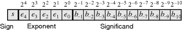
(5.13) 
Nb is the number of bits in the significant and Ne is the number of bits in the exponent. The term subtracted from the exponent is the standard offset or bias that balances the dynamic range so that both a number and its reciprocal may be represented.
The IEEE standard for floating-point numbers (IEEE, 2008) enables reproducibility of floating-point calculations between machines. It does this by specifying the representation (how the bits are encoded) making the floating-point numbers portable. For example, a single precision (32 bit) floating-point number uses 1 bit for the sign, 8 bits for the exponent with an offset of 127, and 24 bits (including the implicit leading 1) for the significand. Two exponent values are reserved for special cases. All zeros are used to represent denormalised numbers (numbers smaller than the smallest normalised number), including zero. All ones are used to represent overflow, infinity and not a number (NaN – for example the result of 0/0 or ![]() ). The standard also specifies how operations should be performed, so that the same calculation should give the same result regardless of the processor performing the computation.
). The standard also specifies how operations should be performed, so that the same calculation should give the same result regardless of the processor performing the computation.
When performing an image processing calculation on an FPGA, the size of the significand and exponent can be tailored to the accuracy of the calculation being performed, to reduce the hardware required. The consequence of this, however, is that the result will, in general, be different from performing the same calculation in software using the IEEE standard. As with fixed-point, this requires a careful analysis of the approximation errors to ensure that the results are meaningful.
Multiplication and division are the most straightforward operations for floating-point numbers. For multiplication, the significands are multiplied and the exponents added. If the resulting significand is greater than two, renormalisation requires shifting it one bit to the right and incrementing the exponent. The product will have more digits than can be represented, so the result must also be rounded to the required number of digits. The sum of the two exponents will include two offsets, so one must be subtracted off. The sign of the output is the exclusive-OR of the input sign bits. Additional logic is required to detect underflow, overflow and handle other error conditions such as processing infinities and NaNs. Division is similar except the significands are divided and the exponents subtracted, and renormalisation may involve a left shift.
Addition and subtraction are more complex. As with the sign-magnitude representation, the actual operation performed will also depend on the signs of the inputs. The numbers must be aligned so that the exponents are the same. This will involve shifting the significand of the smaller number to the right by the difference in the exponents. When implemented on an FPGA, such a shift is either slow (performed as a series of smaller shifts) or expensive (implemented as a large number of wide multiplexers). If available, a multiplier block may also be used to perform the shift (Gigliotti, 2004). It is necessary to keep an extra bit in the shifted smaller number (a guard bit) to reduce the error introduced by the operation (Goldberg, 1991). The significands are then added or subtracted depending on the operation and the result renormalised. If two similar numbers are subtracted, many of the most significant bits may cancel. Renormalisation therefore requires determining the position of the leftmost one, moving this to the most significant bit (both operations may be combined by using the prioritised multiplexer shown in Figure 5.24) and adjusting the exponent accordingly. Again, additional logic is required to handle error conditions.
Floating-point operations require significantly more resources than the corresponding fixed-point operations. It is not that floating point operations are that complicated, but managing the exceptions requires a large proportion of the logic, especially if compliance to the IEEE standard is required. For this reason, most developers prefer to use fixed-point unless the wider dynamic range of floating-point is needed for an application. Where dynamic range is required, one compromise that has been proposed is to use two fixed-point ranges (Ewe et al., 2004, 2005).
5.4.1.2 Logarithmic Number System
An alternative to floating-point is the logarithmic number system, first proposed by Kingsbury and Rayner (1971). This achieves a wide dynamic range by representing a number by its logarithm. A sign-magnitude representation is required because a real logarithm is not defined for negative numbers. The logarithm of zero is also not defined; this requires either a separate flag, a special code or approximating zero by the smallest available number.
The logarithms are usually base-two, although using another base will simply scale the logarithm. The logarithm is represented using fixed-point notation, with NI bits for the integer component and NF bits for the fractional component. The integer component will be the same value as the exponent for a normalised floating-point representation (apart from the offset).
The attraction of the logarithmic number system is that multiplication and division are simple additions and subtractions. If ![]() and
and ![]() then multiplication becomes:
then multiplication becomes:
(5.14) ![]()
Addition and subtraction, however, are more complex. Without loss of generality, assume that A > B. Then:
(5.15) 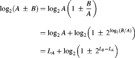
This requires two functions to represent the second term, one for addition:
(5.16) ![]()
and one for subtraction:
(5.17) ![]()
These functions can either be evaluated directly (by calculating ![]() , performing the addition or subtraction, then taking the logarithm), by using table lookup or by piece-wise polynomial approximation (Fu et al., 2006). Since A > B then
, performing the addition or subtraction, then taking the logarithm), by using table lookup or by piece-wise polynomial approximation (Fu et al., 2006). Since A > B then ![]() will be between 0 and 1. Therefore, fAdd will be relatively well behaved, although fSub is more difficult as
will be between 0 and 1. Therefore, fAdd will be relatively well behaved, although fSub is more difficult as ![]() is not defined. The size of the tables depends on NF, and by cleverly using interpolation can be made of reasonable size (Lewis, 1990).
is not defined. The size of the tables depends on NF, and by cleverly using interpolation can be made of reasonable size (Lewis, 1990).
As would be expected, if the computation involves more multiplications and divisions than additions and subtractions then the logarithmic number representation has advantages over floating-point, in terms of both resource requirements and speed (Haselman, 2005; Haselman et al., 2005).
5.4.1.3 Residue Number Systems
A residue number system is a system for reducing the complexity of integer arithmetic by using modulo arithmetic. A set of k co-prime moduli, ![]() , is used and an integer, X, is represented by its residues or remainders with respect to each modulus:
, is used and an integer, X, is represented by its residues or remainders with respect to each modulus: ![]() . That is:
. That is:
(5.18) ![]()
where each ni is an integer and each xi is a positive integer. Negative values of X may be handled just as easily because modulo arithmetic is used. The representation is unique for:
(5.19) 
Addition, subtraction and multiplication are performed respectively by using modulo addition, subtraction and multiplication independently on each of the residues. This makes the residue number system attractive for FPGA implementation (Tomczak, 2006) because it replaces a single wide integer with a set of smaller integers, and the calculations on each of the residues may be implemented in parallel. This can reduce both the propagation delay and logic footprint compared with using wide adders and multipliers.
A disadvantage of the residue number system, however, is that division is impractical. The main application is in digital filtering, which consists of fixed-point multiplications and additions, so the lack of division is not serious.
To be useful, it is necessary to be able to convert from the residue number system back to binary. This is performed using the Chinese remainder theorem or variants (Wang, 1998). A common choice of moduli is ![]() (Wang et al., 2002), for which the logic required to perform modulo arithmetic is only marginally more complex than for performing standard arithmetic. For this set, there are also efficient techniques for converting between binary and the equivalent residue number representation (Fu et al., 2008).
(Wang et al., 2002), for which the logic required to perform modulo arithmetic is only marginally more complex than for performing standard arithmetic. For this set, there are also efficient techniques for converting between binary and the equivalent residue number representation (Fu et al., 2008).
5.4.1.4 Redundant Representations
Arithmetic operations are slow compared to simple logic operations because of the propagation delay associated with the carry from one digit to the next. Another technique that can be used to speed arithmetic is the use of a redundant representation. A redundant number system is one that has more digits than the size of the radix (Avizienis, 1961). Standard binary (radix-2) uses the digits ![]() . A commonly used redundant system is a signed digit representation, where
. A commonly used redundant system is a signed digit representation, where ![]() .
.
With redundancy, carry propagation may be considerably shortened, giving significant speed improvements for additions. A particular signed digit representation that maximises the number of zeroes in the number is the canonical signed digit form (Arno and Wheeler, 1993). This has at least one zero between every non-zero digit, so has at least half of its digits zero. The carry from adding two canonical signed digit numbers will propagate at most one bit. Minimising the number of digits will also reduce the number of partial products when multiplying numbers (Koc and Johnson, 1994).
The disadvantage of redundant representations is that the additional digits require wider signals (at least two bits are required for the radix-2 signed digit representation), wider registers for storing the numbers and, usually, more logic to process the wider signals. While addition of two canonical signed digit numbers will give a signed digit representation, additional logic and propagation delay may be required to convert the result back to canonical form. With any redundant representation, additional logic is required to convert any output back to normal binary.
The signed digit idea can be extended further, for example to ![]() (Sam and Gupta, 1990), to further improve the performance of multipliers in particular. The trade-off is primarily between incremental performance improvements and rapidly increasing circuit complexity. An asymmetric signed digit representation using the digits
(Sam and Gupta, 1990), to further improve the performance of multipliers in particular. The trade-off is primarily between incremental performance improvements and rapidly increasing circuit complexity. An asymmetric signed digit representation using the digits ![]() has been proposed for reducing the number of non-zero digits (Kamp et al., 2006). It also has the advantage that each digit only requires two bits to represent; a single 4-LUT is sufficient to perform an arbitrary operation on two digits (Kamp et al., 2006).
has been proposed for reducing the number of non-zero digits (Kamp et al., 2006). It also has the advantage that each digit only requires two bits to represent; a single 4-LUT is sufficient to perform an arbitrary operation on two digits (Kamp et al., 2006).
Signed digits form the basis of the Booth multiplication algorithm (Booth, 1951), which uses a combination of addition (+1) and subtraction (−1) and nothing (0) to reduce the number of additions required. It is also used by non-restoring division algorithms to avoid having to restore the result when a test subtraction gives a negative result (Bailey, 2006). Redundancy is exploited by SRT division techniques (Robertson, 1958; Tocher, 1958) by giving an overlap when selecting the correct quotient digit. The overlap means that the quotient digit may be determined from an approximation of the partial remainder and does not need to wait for the carry to propagate fully. Similar techniques have also been applied to shift and add methods for the calculation of logarithms and exponentials (Nielsen and Muller, 1996).
5.4.2 Lookup Tables
Many functions can be quite expensive to calculate. In some circumstances, an alternative is to precalculate the function for the range of expected inputs and store the results in a table. Then, rather than calculate the function, the input is simply looked up in the table, which will return the result.
There are two primary instances when the use of lookup tables can be particularly valuable. The first is when the latency of performing the calculation exceeds the available time constraint. Using a lookup table requires a single clock cycle for the memory access regardless of the complexity of the function. The second is when the complexity of the calculation is such that excessive resources are used on the FPGA. A lookup table only requires a memory sufficiently large to provide an accurate representation of the function.
There are two measures commonly used for assessing the accuracy of the representation. Let f(x) be the function that is being approximated and ![]() the approximation in the domain
the approximation in the domain ![]() . The error of the approximation is then:
. The error of the approximation is then:
(5.20) ![]()
The total squared error between the function and its approximation is then:
(5.21) 
A small squared error is one indication of a good approximation.
One limitation of using the square error to measure the difference between the function and its approximation is that minimising the total error can make the absolute error large at some points. Therefore, it is usually better to minimise the maximum absolute error (de Dinechin and Tisserand, 2001), given by:
The difference between minimising the squared error and maximum error is illustrated in Figure 5.29, in particular in the first segment.
Figure 5.29 Approximating a function by lookup table. Left: minimising the mean square error of the function; centre and right: minimising the maximum error; right: reducing the error by increasing the table size.
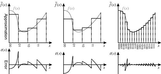
With lookup tables, there is a trade-off between accuracy and the size of the table. While lookup tables can be very efficient for low to moderate accuracy, they do not scale well, with the table size increasing exponentially with the width of the input. Practical table sizes require reducing the accuracy of the input. This can be achieved simply by dropping the least significant bits. It is not necessary to round the input, as the content of the table can be set to give the best result over the domain implied by the bits that are kept. This is clearly shown in the centre panel of Figure 5.29, where the table entry is set to the middle of the range for a particular bit combination. The error depends on the slope of f(x), with the maximum slope determining the number of bits required on the input to achieve a particular accuracy on the output.
5.4.2.1 Interpolated Lookup Tables
Observe that the error function consists of a set of approximately linear segments. This can be exploited by using linear interpolation. Rather than each entry in the table being a constant, each entry can be a line segment containing an intercept, c, and slope, m. The most significant bits are looked up to get the intercept and slope for the corresponding segment, with the least significant bits used to scale the slope to interpolate the values:
The linear segment approximation and corresponding hardware (Mencer and Luk, 2004) are shown in Figure 5.30. The lookup tables for the intercept and slope have the same addresses. Such tables in parallel are effectively a single table with a wider data path. Note that it is not necessary for the piece-wise linear segments to be continuous; smaller errors can in general be obtained by fitting each segment independently. The slope with the smallest error in the sense of Equation 5.22 will, in general, be the slope between the two endpoints, with the segment offset so that the maximum error within the segment is the negative of the error at the ends, as shown on the right in Figure 5.30. Additional errors (not shown in the figure) will arise from truncation of the least significant bits after the multiplication and also the finite precision of the slopes stored in the table.
Figure 5.30 Linearly interpolated lookup table. The table contains both the slope and the intercept. Centre: the computational architecture; right: method of construction that minimises the maximum error.
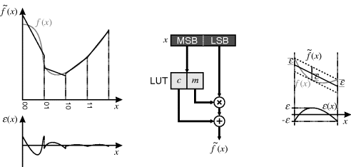
An interpolated table effectively trades the size of the lookup table for increased computational resources and latency. The accuracy of the approximation will depend on the curvature or the second derivative of f(x).
Where the curvature is higher, a smaller step size (more bits used to look up the segment) is required to maintain accuracy. However, over much of the table, the accuracy is more than adequate and a larger step size could be used. A variable step size (effectively varying the partition between the most significant bits looked up and the least significant bits used for the interpolation) can significantly reduce the table size (Lee et al., 2003b; Lachowicz and Pfleiderer, 2008). The cost is a little more logic to manage the variable partitioning. The variable step size approach may be extended to functions of two variables (Nagayama et al., 2008). With two variables, it is essential to partition the space carefully to avoid excessive table sizes, especially for higher precision outputs.
If the approximation is made continuous, as shown in Figure 5.31, and dual-port memory is available for implementing the lookup table, then the slope table is not needed. The current intercept and the next intercept are both looked up using separate ports, and the slope calculated from the difference (Gribbon et al., 2003):
Figure 5.31 Linearly interpolated lookup table using dual-port RAM. The slope is calculated from successive table entries.
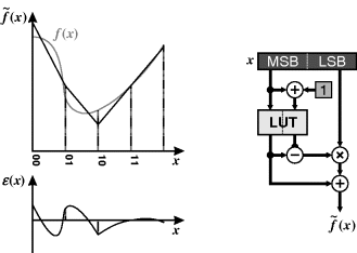
(5.24) ![]()
where ![]() is the weight of the least significant bit used to address the lookup table. The
is the weight of the least significant bit used to address the lookup table. The ![]() is a bit shift, which is free in hardware (hence it is not shown in Figure 5.31). The approximation error may be slightly larger than if each segment is fitted independently, but this will only occur if the second derivative changes sign, as shown between the first two segments in Figure 5.31.
is a bit shift, which is free in hardware (hence it is not shown in Figure 5.31). The approximation error may be slightly larger than if each segment is fitted independently, but this will only occur if the second derivative changes sign, as shown between the first two segments in Figure 5.31.
For higher accuracy, each segment of the table may be represented by a higher order polynomial approximation. This extends Equation 5.23 to:
(5.25) ![]()
where d is the order of the polynomial with coefficients pi. In practise, to control the accumulation of round-off errors, the polynomial should be evaluated using Horner's method:
(5.26) ![]()
For each segment, the optimum polynomial coefficients may be determined using Remez's exchange algorithm (Lee et al., 2003a). As with a linear approximation, the table size can often be significantly reduced by using non-uniform segment widths at the expense of additional decoding logic (Lee et al., 2003a). A higher order polynomial requires fewer segments to fit to a given level of accuracy, but requires more multipliers and, therefore, more resources. It is possible to implement a second order approximation using only a single multiplier by making careful use of lookup tables (Detrey and de Dinechin, 2004).
5.4.2.2 Bipartite and Multipartite Tables
Observe that in Figure 5.30 the slope of the last two segments is very similar. This is often the case, especially with smoothly varying functions. The average slope of the last two segments would also give reasonable errors. If the offsets resulting from multiplying the slope by the least significant bits were stored in a table, the multiplication can be avoided. Unfortunately, if the offsets were stored for every segment, the length of the offset table would be the same as looking up every value. However, since the offsets for adjacent segments are similar (because the slopes are similar) then several of these offsets can be shared between segments, giving a significant reduction in the size of the table.
This is the same concept that is used in tables of logarithms (Hassler and Takagi, 1995). Consider a standard four digit (decimal) table of logarithms. Such a table would require 104 or 10 000 entries. Instead, it is arranged as a two-dimensional grid, with 100 rows indexed by the first two digits and 10 columns indexed by the third digit. A second table, which contains offsets, has the same 100 rows indexed by the first two digits, also with 10 columns, but this time indexed by the fourth digit. The same offsets apply to the whole row of the first table. This dual table approach only requires 1000 entries in each table, for a total of 2000 entries. The savings are even greater than first appear, because the numbers in the second table are smaller, so the bit width can be narrower.
This approach to bipartite tables (Das Sarma and Matula, 1995; Hassler and Takagi, 1995) is shown in Figure 5.32. In this example, the eight segments are split into two groups of four for the offset table. Note that at this scale the bipartite method is not particularly effective for the left group, but works well for the right group where the slopes are similar. In general, the input word is split into three approximately equal groups of bits. The most significant two groups are used to index the main table, and define the segments. The most significant and least significant groups are used to give the offsets that apply to the set of segments defined by the first group.
Figure 5.32 Bipartite lookup tables. Right: symmetry is exploited to reduce the table size.
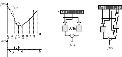
Since no multiplication is used, only an addition, bipartite tables are fast and relatively resource efficient. In addition, since the offsets are usually small, the width of the offset table is usually less than that of the main table. If the value in the main table represents the centre of the segment, the entries in the offset table may be made symmetrical. With a little extra logic, this symmetry may be exploited to halve the size of the offset table (Schulte and Stine, 1997). One of the input bits indicates whether the input value is in the left or right part of a segment. It can therefore be used to invert (using exclusive OR gates) the other address bits within the segment to get the corresponding symmetrical position. The offset from the table is also inverted to give the symmetrical offset, as shown on the right in Figure 5.32.
This idea may be extended further to give multiple tables in parallel (Stine and Schulte, 1999; de Dinechin and Tisserand, 2001), which enables the size of the tables to be reduced further, at the cost of an increased number of additions.
Overall, it has been shown (Boullis et al., 2001; Mencer and Luk, 2004) that for short inputs (up to about 8–10 bits) a direct table lookup is best. For intermediate size inputs (10–12 bits) the bipartite tables require the smallest resources. However, for larger inputs (12–20 bits) interpolated lookup tables are the best compromise.
5.4.3 CORDIC
CORDIC (Coordinate Rotation Digital Computer; Volder, 1959) is an iterative technique for evaluating elementary functions. It was originally developed for trigonometric functions (Volder, 1959), but was later generalised to include hyperbolic functions and multiplication and division (Walther, 1971). For trigonometric functions, each iteration is based on rotating a vector (x, y) by an angle ![]() :
:
The trick is choosing the angle and rearranging Equation 5.27 so that the factors within the matrix are successive negative powers of two, enabling the multiplications to be performed by simple shifts.
(5.28) 
where the direction of rotation, dk, is +1 for an anticlockwise rotation and −1 for a clockwise rotation, and the angle is given by:
After a series of K rotations, the total angle rotated is the sum of the angles of the individual rotations:
(5.30) ![]()
The total angle will depend on the particular rotation directions chosen at each iteration. Therefore, it is useful to have an additional register (labelled z) to accumulate the angle.
The resultant vector is:
(5.31) 
where the scale factor, G, is the gain of the rotation and is constant for a given number of iterations.
(5.32) ![]()
The iterations are, therefore:
with the corresponding circuit shown in Figure 5.33. On Load, the initial values are loaded into the x, y and z registers, and k is reset to zero. Then with every clock cycle, one iteration of summations is performed and k incremented. Note that it is necessary for the summations and the registers to have an extra ![]() guard bits to protect against the accumulation of rounding errors (Walther, 1971). The most expensive part of this circuit is the shifters, which are often implemented using multiplexers. If the FPGA has available spare multipliers, these may be used to perform the barrel shifts (Gigliotti, 2004). A small ROM is required to store the small number of angles given by Equation 5.29. There are two modes for choosing the direction of rotation at each step (Volder, 1959): rotation mode and vectoring mode.
guard bits to protect against the accumulation of rounding errors (Walther, 1971). The most expensive part of this circuit is the shifters, which are often implemented using multiplexers. If the FPGA has available spare multipliers, these may be used to perform the barrel shifts (Gigliotti, 2004). A small ROM is required to store the small number of angles given by Equation 5.29. There are two modes for choosing the direction of rotation at each step (Volder, 1959): rotation mode and vectoring mode.
Figure 5.33 Iterative hardware implementation of the CORDIC algorithm.
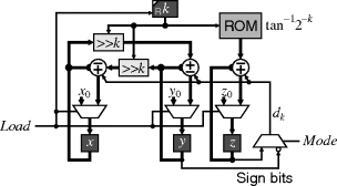
The rotation mode starts with an angle in the z register and reduces this angle to zero by choosing dk as the sign of the z register as the vector is rotated:
The result after K iterations is:
This converges (zK can be made to go to zero within the precision of the calculation; Walther, 1971) if:
(5.36) ![]()
In other words, if the angle is zero, and a rotation moves it away, the remaining rotations must be able to move it back to zero again. In this case, the series converges because:
(5.37) ![]()
For Equation 5.33 the domain of convergence is:
Starting with ![]() and
and ![]() , the rotation mode can be used to calculate the sine and cosine of the angle in z0. It may also be used to rotate a vector by an angle, subject to the extension of the magnitude by a factor of G. For angles larger than 90°, the easiest solution is to perform an initial rotation by 180°:
, the rotation mode can be used to calculate the sine and cosine of the angle in z0. It may also be used to rotate a vector by an angle, subject to the extension of the magnitude by a factor of G. For angles larger than 90°, the easiest solution is to perform an initial rotation by 180°:

The second mode of operation is vectoring mode. This chooses dk as the opposite of the sign of the y register, determining the angle required to reduce y to zero:
which gives the result:
(5.41) 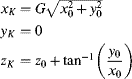
This has the same domain of convergence as the rotation mode, given in Equation 5.38. Therefore, if ![]() it is necessary to bring the vector within range by rotating by 180° (Equation 5.39). The vectoring mode effectively converts a vector from rectangular to polar coordinates. If x0 and y0 are both small, then rounding errors can become significant, especially in the calculation of the arctangent (Kota and Cavallaro, 1993). If necessary, this may be solved by renormalizing xk and yk by scaling by a power of two (a left shift).
it is necessary to bring the vector within range by rotating by 180° (Equation 5.39). The vectoring mode effectively converts a vector from rectangular to polar coordinates. If x0 and y0 are both small, then rounding errors can become significant, especially in the calculation of the arctangent (Kota and Cavallaro, 1993). If necessary, this may be solved by renormalizing xk and yk by scaling by a power of two (a left shift).
With both the rotation mode and vectoring mode, each iteration improves the accuracy of the angle by approximately one binary digit.
An additional mode of operation has been suggested by Andraka (1998) for determining arcsine or arccosine. It starts with x0 = 1 and y0 = 0 and rotates in the direction given by:
(5.42) ![]()
where s is the sine of the angle. The result after converging is:
(5.43) 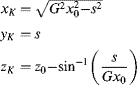
This result would be simpler if initialised with ![]() . This mode is effective for
. This mode is effective for ![]() . Outside this range, the gain of the rotation can cause the wrong direction to be chosen, leading to convergence failure (Andraka, 1998). An alternative two-step approach to calculating arcsine and arccosine will be described shortly.
. Outside this range, the gain of the rotation can cause the wrong direction to be chosen, leading to convergence failure (Andraka, 1998). An alternative two-step approach to calculating arcsine and arccosine will be described shortly.
One way of speeding up CORDIC is to consider the Taylor series expansions for sine and cosine for small angles (Walther, 2000):
(5.44) 
After N/2 iterations in the rotation mode, the angle in the z register is such that ![]() is less than the significance of the least significant guard bit, so can be ignored. The remaining N/2 iterations may be replaced by small multiplications:
is less than the significance of the least significant guard bit, so can be ignored. The remaining N/2 iterations may be replaced by small multiplications:
(5.45) ![]()
(The assumption here is that the angle is in radians.) Note that the same technique cannot be applied in the vectoring mode because it relies on the angle approaching zero.
The implementation in Figure 5.33 is word-serial in that each clock cycle performs one iteration at the word level. Other implementations are the bit-serial (Andraka, 1998) and the unrolled parallel versions (Wang et al., 1996; Andraka, 1998). The bit-serial implementation uses significantly fewer resources, but requires N clock cycles per iteration, where N is the width of the registers. The unrolled implementation (Figure 5.34) uses separate hardware for each iteration and can perform one complete calculation per clock cycle. Unrolling enables two simplifications to the design. Firstly, the shifts at each iteration are fixed and can be implemented simply by wiring the appropriate bits to the inputs to the adders. Secondly, the angles that are added are constants, simplifying the z adders.
Figure 5.34 Unrolled CORDIC implementation.
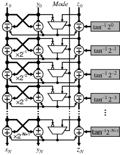
The propagation delay of the unrolled implementation is long because the carry must propagate all of the way to the sign bit at each iteration before selecting the next operation. However, the design can be readily pipelined with a throughput of one calculation per clock cycle. Several attempts have been made at reducing the latency by investigating ways of overcoming the carry propagation. It cannot be solved using redundant arithmetic, because to determine the sign bit with redundant arithmetic it is still necessary to propagate the carry. Two approaches have been developed, although they only work in rotation mode. The first is to work with the absolute value in the z register and detect the sign changes (Dawid and Meyr, 1992), which can be done with redundant arithmetic, working from the most significant bit down, significantly improving the delay. The second approach relies on the fact that the angles added to the z register are constant, enabling dk to be predicted, significantly reducing the latency (Timmermann et al., 1992).
5.4.3.1 Compensated CORDIC
A major limitation of the CORDIC technique is the rotation gain. If necessary, this constant factor may be removed by a multiplication either before or after the CORDIC calculation. Compensated CORDIC algorithms integrate this multiplication within the basic CORDIC algorithm in different ways.
Conceptually the simplest (and the original compensated CORDIC algorithm) is to introduce a scale factor of the form ![]() with each iteration (Despain, 1974). The sign is chosen so that the combined gain approaches one. This can be generalised in two ways. The first is by applying the scale factor only on some iterations, and choosing the terms so that the gain is two, enabling it to be removed with a simple shift. Since the signs are predetermined, this results in only a small increase in the propagation delay, although the circuit complexity is considerable increased.
with each iteration (Despain, 1974). The sign is chosen so that the combined gain approaches one. This can be generalised in two ways. The first is by applying the scale factor only on some iterations, and choosing the terms so that the gain is two, enabling it to be removed with a simple shift. Since the signs are predetermined, this results in only a small increase in the propagation delay, although the circuit complexity is considerable increased.
The second approach is to repeat the iterations for some angles to drive the total gain, G, to two (Ahmed, 1982). This uses the same hardware as the original CORDIC, with only a little extra logic required to control the iterations. The disadvantage is that it takes significantly longer than the uncompensated algorithm. A hybrid approach is to use a mixture of additional iterations and scale factor terms to reduce the total logic required (Haviland and Tuszynski, 1980). This is probably best applied to the unrolled implementation.
Another approach is to use a double rotation (Villalba et al., 1995). This technique is only applicable to the rotation mode; it performs two rotations in parallel (with different angles) and combines the results. Consider rotating by an angle ![]() :
:
(5.46) ![]()
Similarly, rotating by an angle ![]() gives:
gives:
(5.47) ![]()
Then adding these two results cancels the terms containing ![]() :
:
(5.48) 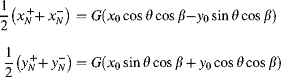
Therefore, by setting ![]() , the gain term can be completely cancelled. It takes the same time to perform the double rotation as the original CORDIC apart from the extra addition at the end. However, it does require twice the hardware to perform the two rotations in parallel, and this technique does not work for the vectoring mode.
, the gain term can be completely cancelled. It takes the same time to perform the double rotation as the original CORDIC apart from the extra addition at the end. However, it does require twice the hardware to perform the two rotations in parallel, and this technique does not work for the vectoring mode.
5.4.3.2 Linear CORDIC
So far the discussion of CORDIC has been in a circular coordinate space. The CORDIC iterations may also be applied in a linear space (Walther, 1971):
(5.49) ![]()
Again, either the rotation mode or vectoring mode may be used. Rotation mode for linear CORDIC reduces z to zero using Equation 5.34, and in doing so is performing a variation on long multiplication with the result:
(5.50) 
The domain of convergence depends on the initial value of k.
(5.51) ![]()
Vectoring mode reduces y to zero using Equation 5.40 and effectively performs the same algorithm as non-restoring division, with the result:

Usually, ![]() for which Equation 5.52 will converge provided
for which Equation 5.52 will converge provided ![]() . Note that there is no scale factor or gain term associated with linear CORDIC.
. Note that there is no scale factor or gain term associated with linear CORDIC.
5.4.3.3 Hyperbolic CORDIC
Walther (Walther, 1971) also unified CORDIC with a hyperbolic coordinate space. The corresponding iterations are then:
(5.53) 
There are convergence issues with these iterations that require certain iterations to be repeated (![]() ) (Walther, 1971). Note, too, that the iterations start with
) (Walther, 1971). Note, too, that the iterations start with ![]() because
because ![]() .
.
Subject to these limitations, operating in rotation mode gives the result:
(5.54) 
where the gain factor (including the repeated iterations) is:
(5.55) ![]()
and the domain of convergence is:
(5.56) ![]()
Operating in vectoring mode gives the result:
(5.57) 
As with circular CORDIC, the gain may be compensated either by appropriate initialisation of the x or y register (for rotation mode) or by introducing additional, compensating operations. Much of the discussion of compensated CORDIC above may be adapted to hyperbolic coordinates.
The CORDIC iterations from the different coordinate systems may be combined to use the same hardware (with a multiplexer to select the input to the x register). With all three modes available, other common functions may also be calculated (Walther, 1971):
(5.58) ![]()
(5.59) ![]()
(5.60) ![]()
(5.61) ![]()
(5.62) ![]()
Other common functions that may be calculated in two steps are:
(5.63) ![]()
(5.64) ![]()
5.4.3.4 CORDIC Variations and Generalisations
The basis behind CORDIC is to reduce multiplications by an arbitrary number to a shift by constraining the system to powers of two. This can be extended to the direct calculation of other functions. For example, looking at logarithmic functions (Specker, 1965), the relation:
(5.65) ![]()
allows a shift and add algorithm for the calculation of logarithms. The idea is to successively reduce x to one by a series of multiplications, and adding the corresponding logarithm terms obtained from a small table. The iteration is given by:
(5.67) ![]()
will converge for ![]() to:
to:
(5.68) ![]()
Alternatively, if a factor of ![]() is used, then the iteration converges for
is used, then the iteration converges for ![]() . The iteration of Equation 5.66 may also be readily adapted to taking logarithms in other bases simply by changing the table of constants added to the z register. The algorithm can also be run the other way, by reducing zk to zero, giving the exponential function.
. The iteration of Equation 5.66 may also be readily adapted to taking logarithms in other bases simply by changing the table of constants added to the z register. The algorithm can also be run the other way, by reducing zk to zero, giving the exponential function.
Muller (1985) showed that this iteration shared the same theory as the CORDIC iteration and placed them within the same framework. Since trigonometric functions can be derived from complex exponentials using the Euler identity:
(5.69) ![]()
the iteration of Equation 5.66, can be generalised to use complex numbers (Bajard et al., 1994) enabling trigonometric functions to be calculated without the gain factors associated with CORDIC. Another advantage of this implementation is that it allows redundant arithmetic to be used (Nielsen and Muller, 1996) by exploiting the fact that if ![]() then there is an overlap between the selection ranges for the dk. This means than only the few most significant bits need to be calculated in order to determine the next digit, reducing the effects of carry propagation delay.
then there is an overlap between the selection ranges for the dk. This means than only the few most significant bits need to be calculated in order to determine the next digit, reducing the effects of carry propagation delay.
While the CORDIC and other related shift-and-add based algorithms have relatively simple circuitry, their main limitation is their relatively slow rate of convergence. Each iteration gives only a single bit improvement of the result. A further limitation is that only a few elementary functions may be calculated. More complex or composite functions require the evaluation of many elementary functions.
5.4.4 Approximations
An alternative to direct function evaluation is to approximate the function with another simpler function that gives a similar result over some domain of interest. One popular method of approximating functions is to use a minimax polynomial. This chooses the polynomial coefficients to minimise the maximum approximation error within the domain of interest:
(5.70) ![]()
Typically, Remez's exchange algorithm is used to find the coefficients. However, such coefficients do not take into account the fact that it is desirable to perform the calculation with limited precision or small multipliers, and simply rounding the coefficients may not give the coefficients with minimum error (Brisebarre et al., 2006). This requires a search for the appropriate coefficients.
For low precision outputs (less than 14–20 bits) table lookup methods are both faster and more efficient (Sidahao et al., 2003). However, the resources to implement a lookup table grow exponentially with output precision, whereas those required for polynomial approximations grow only linearly.
An extension of polynomial approximations are rational approximations where:
(5.71) 
For a given level of accuracy, a lower order rational polynomial is required (Koren and Zinaty, 1990) than a regular polynomial, although it does require a division operation. This makes rational polynomial approximations best suited for high precision.
A further approach for high precision is to use an iterative approximation. This starts with an approximate solution and with each iteration improves the accuracy. A common approach is the Newton–Raphson iteration, which is a root-finding algorithm. The Newton–Raphson iteration is given by:
It works, as illustrated in Figure 5.35, by projecting the slope at xk to obtain a more accurate estimate.
Figure 5.35 Newton–Raphson iteration.
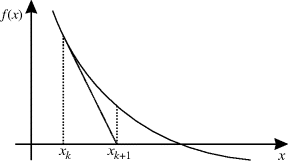
Newton–Raphson has quadratic convergence. This means that if the input is close to the solution, the relative error will square with each iteration. This effectively means that the number of significant bits will approximately double with each iteration.
For example, to evaluate the square root of an input number, X, an equation is formed for which ![]() is a root:
is a root:
(5.73) ![]()
Then, the iteration is formed from Equation 5.72:
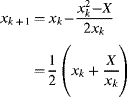
Note that the iteration of Equation 5.74 requires a division, which is relatively expensive. A variation on this technique is to rearrange the equation to be solved. For example:
(5.75) ![]()
so solving ![]() enables
enables ![]() to be calculated with a final multiplication. The corresponding function to solve would be:
to be calculated with a final multiplication. The corresponding function to solve would be:
(5.76) ![]()
with the corresponding iteration:
Although Equation 5.77 is more complex than Equation 5.74, it does not involve a division and can almost certainly be implemented with lower latency.
The number of iterations required to reach a desired level of accuracy depends on the accuracy of the initial estimate. Therefore, other techniques, such as lookup tables or other approximations, are helpful to give a more accurate initial approximation and hence reduce the number of iterations (Schwarz and Flynn, 1993). Since the iteration for many functions is a polynomial (for example Equation 5.77), the same hardware may be used to form the initial approximation using a low order polynomial (Habegger et al., 2010).
5.4.5 Other Techniques
5.4.5.1 Bit-Serial Processing
In situations where resources are scarce but latency is less of an issue, bit-serial processing can provide a solution. Conventionally, operations are performed a whole word at a time, processing all of the bits within a data word in parallel. In contrast to this, bit-serial techniques process the data one bit per clock cycle (Denyer and Renshaw, 1985). This requires serialising the input data and processing the data as a serial bit-stream. The order that the bits should be presented (least significant bit first, or most significant bit first) will depend on which input bits affect which output bits (Andraka, 1996). For example, most arithmetic operations should be presented least significant bit first because carry propagates from the lower bits to the higher bits. This is illustrated in Figure 5.36 for a bit-serial adder.
Figure 5.36 Bit-serial adder.
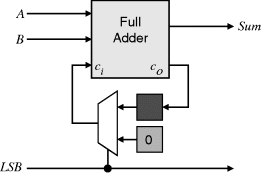
Processing only one bit at a time can significantly reduce the propagation delay, although more clock cycles are required to process the whole word. For many operations, bit-serial processing can lead to efficient pipelined designs or systolic structures. Another significant advantage of bit-serial designs is that, because the logic is more compact, routing is also simplified and more efficient (Isshiki and Dai, 1995).
A compromise between bit-serial and word-parallel systems is digit-serial designs (Parhi, 1991). These process a small number of bits (a digit) in parallel but have the digits presented serially. This can reduce the high clock speeds required for bit-serial designs while maintaining efficient use of logic resources. Digit-serial designs therefore fall within the spectrum between bit-serial and word-parallel systems.
5.4.5.2 Incremental Update
Another technique that may be employed, particularly with stream processing, is incremental update. Rather than perform a complete calculation independently for each pixel, incremental update exploits the fact that often part of the calculation performed for the previous pixel may be reused. A classic example (Gribbon et al., 2003) is the calculation of x2 or y2 where x and y are pixel coordinates. When moving to the next pixel, the identity:
(5.78) ![]()
can be used to maintain the value of x2 without performing a multiplication. The same concept may be extended to calculate higher order moments (Chan et al., 1996).
A similar technique may be used to determine the input location for an affine transformation incrementally. Consider the transformation:
(5.79) 
The input location corresponding to the next pixel in the scan line is then given by:
(5.80) ![]()
Note that in this case it may be necessary to keep extra guard digits to prevent accumulation of round-off errors in the approximation of A and D.
Another common example of incremental update is with local filters. As the window moves from one pixel to the next, there is a significant overlap between the corresponding input windows. Many of the pixels within the window will be the same as the window moves. This may be exploited, for example, by median filters by maintaining a histogram of the values within the window and updating the histogram only for the pixels that change (Garibotto and Lambarelli, 1979; Huang et al., 1979; Fahmy et al., 2005).
5.4.5.3 Separability
Image processing often involves operations that require inputs from two (or more) dimensions. Separable operations are those that can split the two-dimensional operations into separate operations in each of the X and Y dimensions. The separate one-dimensional operations are usually significantly simpler than the composite two-dimensional operation. The most common application of separability is with filters, but it can also be applied to two-dimensional transformations such as the fast Fourier transform (FFT), or be used with image warping (Catmull and Smith, 1980).
This chapter has reviewed a range of techniques for mapping from a software algorithm to a hardware implementation. These techniques may be considered as a set of design patterns that provides ways of overcoming common problems or constraints encountered in the mapping process (DeHon et al., 2004; Gribbon et al., 2005; 2006).
Timing constraints focussed particularly on the limited time available for performing the required operations. One technique for improving throughput is to use low level pipelining. Another timing issue encountered with concurrent systems is the synchronisation of the different processes. For synchronous processes, global scheduling can derive synchronisation signals from a global counter. With asynchronous systems one synchronisation technique is to use a channel based on CSP. If necessary, a FIFO can be used to smooth the flow of data between processes.
Memory bandwidth constraints result from the fact that only one memory access may be made per clock cycle. A range of techniques were reviewed that improved the bandwidth of external memories. The largest effect can be obtained by caching data on the FPGA where the data may be distributed over several parallel block RAMs, significantly increasing the bandwidth. Custom caching can significantly reduce the number of times that the data needs to be loaded into the FPGA.
The third form of constraint was for resources. Any concurrent system with shared resources will face contention when a resource is used by multiple processes. The resource needs to be multiplexed between the various processes, with appropriate conflict arbitration. This is best managed by combining the resource with its manager. Efficient use of the limited logic and memory resources available on an FPGA requires appropriate data structures and computational techniques to be used by the algorithm. If necessary, the FPGA can be dynamically reconfigured to switch from one task to another. While partial reconfigurability has received a lot of research, not every FPGA supports it, and those that do require quite low level programming to manage the placement constraints.
The next several chapters explore how these may be specifically applied to mapping image processing operations onto an FPGA. Every operation may be implemented in many different ways. However, the primary focus is on stream processing where appropriate. This is because, for an embedded system, the data is inevitably streamed from a camera or other device. If the data is processed as it is streamed in, the memory requirements of the algorithm can often be significantly reduced. Using stream processing does place a strict time constraint of a one pixel per clock cycle (although this may be relaxed a little for slower pixel clocks by using multiphase techniques), so not every operation may be able to be streamed.