
2.4 Characteristic Impedance
Figure 2.3 shows how a wave propagates when a voltage with a finite rise time is switched on to a length of transmission line.
Figure 2.3 How a step voltage propagates on an ideal transmission line.
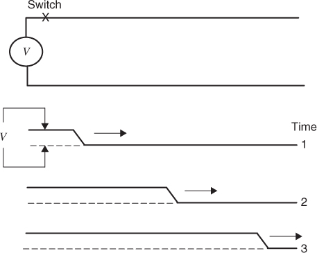
This line can be characterized as having an inductance and a capacitance per unit length. The step wave that propagates down the line will place charges on the distributed capacitance at a fixed rate. After the wave is established, a steady current is supplied by the voltage source. A steady voltage and a steady current imply that the transmission line looks like a resistance. This resistance value is called the characteristic impedance of the line. If the line is infinite in length, the current–voltage relationship will be given by Ohm's law as
where Z0 is the characteristic impedance.
In theory, the voltage V can have any wave form. In digital circuits, logic voltages are step functions with finite rise and fall times. In rf (analog) circuits, the signals are usually sine waves.
The characteristic impedance of a transmission line is given by
where L and C are the inductance and capacitance per unit length, respectively. In circuit board designs, the characteristic impedance of each logic trace must be considered. This practice provides uniformity in terms of reflections, current demands, and losses. Very accurate control is not practical, as there are many side effects that influence the impedance. For example, the dielectric constant will vary between boards and in different areas of the same board. Nearby traces will modify the impedance. Trace dimensions will vary during manufacturing, and this directly influences the characteristic impedance. The amount of dielectric material around a trace will vary with location. Dielectrics can include conformal coatings, coupons, and, to some extent, moisture.
The characteristic impedance of a transmission line is equal to the ratio between the E and H fields at every point in the space near the conductors. This ratio holds for every wave that is in motion on the line. The ratio of E to H inside of traces is different. Stating this in another way, a transmission line will only support waves with a fixed wave impedance.
Equations for the characteristic impedance of trace geometries are available from many sources. These sources include trade publications, books, the internet, engineering service organizations, and hardware planners. A few equations are supplied in Chapter 6 of this book. Typically, traces on a circuit board have characteristic impedances around 50 ohm. This value turns out to be effective for most designs. Higher impedances invite cross talk and lower impedances place extra demands on the current supplied by the logic. For some logic families, the optimum characteristic impedance may be other than 50 ohm. It is perfectly acceptable to design a board where different trace groups have different characteristic impedances.