
CHAPTER 9
INTERRUPTS AND A FIRST LOOK AT TIMERS
This chapter discusses interrupts, which are of critical importance when implementing efficient input/output operations for microcontroller applications. Topics include interrupt fundamentals, PIC24 μC interrupt sources, and an introduction to using interrupts for accomplishing I/O. A first look at the powerful timer subsystem of the PIC24 μC uses a timer as a periodic interrupt source.
Learning Objectives
After reading this chapter, you will be able to:
![]() Discuss the general function of interrupts within a microprocessor and interrupt implementation on the PIC24 μC.
Discuss the general function of interrupts within a microprocessor and interrupt implementation on the PIC24 μC.
![]() Describe the difference between polled I/O and interrupt-driven I/O.
Describe the difference between polled I/O and interrupt-driven I/O.
![]() Implement an interrupt service routine in C for the PIC24 μC.
Implement an interrupt service routine in C for the PIC24 μC.
![]() Implement an interrupt service routine using a state machine approach.
Implement an interrupt service routine using a state machine approach.
![]() Implement interrupt service routines that use the change notification and INTx interrupts.
Implement interrupt service routines that use the change notification and INTx interrupts.
![]() Discuss the structure of the PIC24 μC Timer2 and Timer3 subsystems and use them to generate periodic interrupts for input sampling.
Discuss the structure of the PIC24 μC Timer2 and Timer3 subsystems and use them to generate periodic interrupts for input sampling.
![]() Implement an interface for a rotary encoder.
Implement an interface for a rotary encoder.
![]() Implement an interface for a keypad.
Implement an interface for a keypad.
Interrupt Basics
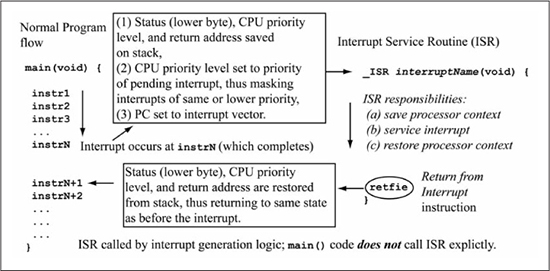
An interrupt in a microprocessor is a forced deviation from normal program flow by an external or internal event. On the PIC24 μC there are many possible internal and external events such as rising or falling edges on external pins, arrival of serial data, timer expiration, and so forth that can cause interrupts. Figure 9.1 illustrates what happens when an interrupt occurs on the PIC24 μC. During normal program flow, assume some external or internal event triggers an interrupt. After the current instruction is finished, the CPU interrupt priority level (discussed later), lower byte of the status register, the stack frame active bit, and the return address are pushed on the stack. The CPU interrupt priority level is then set to the priority level of the pending interrupt, and the PC is set to a predetermined location based on the pending interrupt called the interrupt vector, thus causing execution to continue at that point. After executing code to handle the interrupt, a retfie (return from interrupt) instruction is executed to return to normal program flow. The code that is executed when the interrupt occurs is referred to as the interrupt service routine (ISR). The ISR’s function is to respond to whatever event triggered the interrupt. As an example, if the interrupt was triggered by the arrival of serial input data, the ISR would read the data, save it, then return. When viewing Figure 9.1, it is tempting to think of the ISR as a subroutine that is called by the main() program. However, the ISR is never manually called as a normal C function is called; instead, the ISR is invoked automatically by the PIC24 μC interrupt hardware on an interrupt occurrence. An ISR is said to execute in the background, while the normal program flow executes in the foreground. This book informally refers to background code as ISR code execution and foreground code as main() code execution. Saving the processor context in the ISR of Figure 9.1 means to save registers used by the ISR since these same registers can be used by the foreground code. An ISR can call other subroutines, and, in fact, can call a subroutine that has been interrupted. If a subroutine is interrupted, then called from the ISR, the subroutine has been reentered (a reentrant subroutine). For correct execution, a reentrant subroutine must use dynamic allocation for locals and parameters, and the ISR must save the processor context. An ISR can itself be interrupted as is discussed later, so generally the processor context is saved to the stack (dynamic allocation is used for the processor context).
You may question at this point why an interrupt capability is desirable. The I/O examples presented in the last chapter use a technique referred to as polling, where a status flag is checked repeatedly to determine data availability. This is referred to as polled I/O and is usually an inefficient method for implementing I/O operations. Imagine if your cell phone operated on the polled I/O principle. This would mean that you would occasionally have to pull it out of your pocket or purse, open it, and ask “Hello, is there anybody there?” This may seem laughable, but this is how we have been accomplishing I/O to this point. The problem with this approach is obvious—either you check your phone too often, which wastes your time, or you do not check it often enough, causing you to miss an important call. It is much more efficient to have the phone notify you of an incoming call.
The ringer on your cell phone implements an interrupt; when the ringer sounds, you stop what you are doing and answer the phone, thus servicing the interrupt. When finished with the call, you then resume what you were doing earlier. This is known as interrupt-driven I/O. On the PIC24 μC, each interrupt source has an associated interrupt flag bit that becomes a 1 when the interrupt source event occurs. As an example, the U1RXIF bit is the receive character interrupt flag and becomes a 1 when asynchronous serial data is available over the RX serial pin. Most interrupt flag bits are contained in special function registers named the interrupt flag status (IFS) registers.
Continuing the cell phone analogy, there are times when you do not want to answer the phone, like in a meeting or a movie theatre. At these times, you turn off the ringer, causing incoming calls to be ignored. On the PIC24 μC, most interrupt sources have an interrupt enable bit that must be a 1 in order for an interrupt to be invoked when the interrupt flag bit becomes a 1. If the interrupt enable bit is 0, the interrupt is masked or disabled. For example, the U1RXIE bit (receive character interrupt enable) is the interrupt enable for the U1RXIF interrupt. Most interrupt enable bits are contained in special function registers named the interrupt enable control (IEC) registers. It is important to understand that the interrupt enable bit being a 0 does not prevent the interrupt flag bit from becoming a 1, just like turning off the phone ringer does not prevent incoming phone calls from arriving. A 0 interrupt enable bit only prevents an interrupt from being generated; in other words, it prevents a jump to the ISR. Some interrupts on the PIC24 μC are non-maskable, which means that you cannot block the automatic jump to the ISR when the interrupt occurs (for example, a fire alarm can be considered a non-maskable interrupt as it is never disabled).
Figure 9.1
Interrupting normal program flow
At the risk of overusing the cell phone analogy, assume you are talking on the phone with a friend and that you are notified via call-waiting of an incoming call from your spouse, significant other, or other family member. You may say something like “Hold for a moment, there is an incoming call that I need to check,” and then switch to the other call. This means that the incoming call has a higher priority than the current call. On the PIC24 μC, each interrupt source has an interrupt priority level (IPL) associated with it. This interrupt priority level ranges from 0 to 15 and allows interrupts of a higher priority to interrupt lower-priority ISR code. Interrupt priorities are discussed in detail in the next section.
PIC24 μC Interrupt Details
This section discusses PIC24 μC details such as the interrupt vector table, priority system, and the difference between traps and peripheral interrupts.
Vector Table
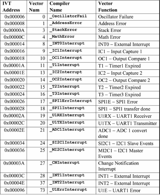
When an enabled interrupt occurs, the PIC24 μC fetches the ISR starting address for that interrupt from the interrupt vector address assigned to that interrupt. The interrupt vector addresses are stored in a group of program memory locations known as the interrupt vector table (IVT), which is shown in Figure 9.2. These locations along with the reset vector occupy locations 0x000004 through 0x0001FF, with user code starting at location 0x000200.
Figure 9.2
Interrupt vector table

Source: Figure redrawn by author from Figure 6.1 of the PIC24E FRM datasheet (DS70600C), Microchip Technology, Inc.
The number of interrupt sources on a PIC24 μC depends on the on-chip peripherals that are implemented for that particular microcontroller. Figure 9.3 shows common interrupt sources on the dsPIC33EP128GP502 which are discussed in this book; the processor supports many additional interrupts. The “Vector Num” column gives the value written to the lower seven bits of the special function register INTTREG (INTTREG<6:0>) for the currently executing interrupt, with bits INTTREG<11:8> containing the interrupt’s priority. (Note: The INTTREG register is not present in the PIC24F family.) The PIC24 “Compiler Name” column gives the C function name that must be used with the PIC24 compiler when writing an ISR for that particular interrupt.
Figure 9.3
Selected dsPIC33EP128GP502 interrupt sources
Interrupt Priorities
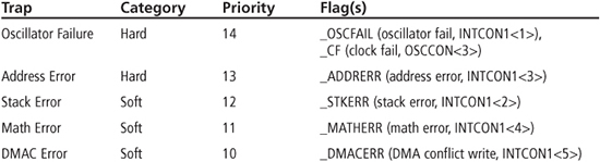
As mentioned previously, the PIC24 μC implements an interrupt priority system with values from 0 (lowest) through 15 (highest). Interrupt priorities 8 through 15 are reserved for a special class of interrupt sources known as traps (vector numbers 1 through 5) with each interrupt priority level assigned to a single trap source. Priorities 0 through 7 are used for non-trap interrupt sources (user interrupts), with each user interrupt source assigned a 3-bit field in a special function register that contains the interrupt’s priority level. These interrupt priority level bits are contained in a set of special function registers known as the interrupt priority control (IPC) registers. The current CPU interrupt priority level is a 4-bit value (IPL<3:0>), with these bits split between two special function registers: IPL<2:0> bits are in the status register (SR<7:5>), while IPL<3> is contained in the core control register (CORCON<3>). The IPL bits are cleared at reset, which means that any enabled interrupt with priority level 1 or higher can interrupt the processor. Bits IPL<2:0> are writeable, but bit IPL<3> can only be cleared by user code (the IPL<3> bit is set when any trap occurs, because trap priorities are 8 and higher).
When an enabled interrupt occurs, the interrupt’s priority level must be higher than the current IPL<3:0> bits to be recognized. If simultaneous interrupts with the same priority level occur, then the interrupt with the lower vector number is recognized first. Before the ISR is executed, the current IPL bits are saved on the stack along with the return address then the IPL bits are set to the priority level of the recognized interrupt. This disables any further interrupts within the ISR caused by interrupts with that priority level. Interrupts of a higher priority can interrupt the ISR. If an ISR is interrupted by another interrupt, this is called interrupt nesting, which can be disabled by setting the interrupt nesting disable bit (NSTDIS, in INTCON1<15>) to a one (_NSTDIS=1). When interrupt nesting is disabled, any user-level interrupt sets the CPU IPL to 7, disabling any further user-level interrupts. Furthermore, the IPL<2:0> bits become read-only and the assigned priority levels for individual interrupts are only used to resolve simultaneous interrupts.
Setting a user interrupt priority to level 0 disables that interrupt even if its interrupt enable bit is set, because the priority level is not greater than the lowest CPU priority level of 0. Setting the IPL<2:0> bits to 7 disables all user interrupts. The DISI #lit14 instruction (disable interrupts temporarily) can be used to disable user interrupts with priorities 1 through 6 for #lit14 + 1 instruction cycles. This is useful for protecting critical code sections from user interrupts, which is done in the configClock() function when the clock source is being changed.
Traps
A special type of interrupt source on the PIC24 μC are traps, which are internally generated, nonmaskable interrupts that immediately halt instruction execution (hard traps) or that allow a few additional instruction to execute before jumping to the ISR (soft traps). Soft trap sources include a DMA conflict write, math error (divide by zero), and stack error (triggers include the stack pointer falling below 0x1000 or becoming greater than the SPLIM register). Hard trap sources include oscillator failure (which occurs if the fail-safe clock monitor detects a problem or if the PLL loses lock) and address error (caused by a misaligned access or a jump or branch to unimplemented program space). Complete details on the trap error sources are given in [14]. Table 9.1 summarizes the trap error sources.
Interrupt Latency
Interrupt latency is the amount of time from when an interrupt occurs to when the interrupt source is handled. In the cell phone analogy, this is the amount of time from when the phone rings until you say “Hello.” In many cases reducing interrupt latency is important; as in the cell phone analogy, if you wait too long to answer the phone, the person calling may give up and terminate the call. Interrupt latency consists of two parts: (1) the time from when the interrupt occurs until the first instruction of the ISR is handled, and (2) the number of instructions executed in the ISR before the interrupt source is acknowledged. When an interrupt occurs, the interrupted instruction completes, then the processor takes fourteen clock cycles on the PIC24E/dsPIC33E before the first instruction of the ISR is executed. The interrupt latency for a two-cycle instruction is also 14 clocks to the first instruction of the ISR, regardless of whether the interrupt occurs in the first or second cycle of the instruction [29].
Once the ISR has begun execution, the latency until the interrupt is serviced depends on how much of the processor state has to be saved within the ISR. A complex ISR may require many working registers to be pushed on the stack at entry to the ISR. The push.s (push shadow registers) instruction that saves W0, W1, W2, W3, and the status register to the stack can help reduce the number of clocks required to save the processor context. There is only one set of shadow registers so an ISR that uses the shadow registers cannot be interrupted by a higher priority interrupt that also uses the shadow registers, or else the values saved to the shadow registers may be corrupted.
Return from interrupt timing consists of two instruction cycles for the retfie instruction plus five instruction cycles on the PIC24E/dsPIC33E to fetch the instruction at the return address; the instruction at the return address is executed on the eighth instruction cycle counting from retfie start.
ISR Overhead
A concern in interrupt processing is the percentage of the CPU’s execution time spent in interrupt service routines. The following definitions will help you compute this percentage.
![]() IENTRY: Number of instruction cycles for ISR entry (fourteen on the PIC24E/dsPIC33E μC; four on the PIC24F/H and dsPIC33F).
IENTRY: Number of instruction cycles for ISR entry (fourteen on the PIC24E/dsPIC33E μC; four on the PIC24F/H and dsPIC33F).
![]() IBODY: Number of instruction cycles for the ISR body (not including
IBODY: Number of instruction cycles for the ISR body (not including retfie).
![]() IEXIT: Number of instruction cycles for ISR exit (seven on the PIC24E/dsPIC33E μC; three on the PIC24F/H and dsPIC33F).
IEXIT: Number of instruction cycles for ISR exit (seven on the PIC24E/dsPIC33E μC; three on the PIC24F/H and dsPIC33F).
![]() FISR: Frequency (number of times per second) at which the ISR is triggered.
FISR: Frequency (number of times per second) at which the ISR is triggered.
![]() TISR: The ISR triggering period, which is 1/FISR. For example, if an ISR is executed at 1 KHz, TISR is 1 ms.
TISR: The ISR triggering period, which is 1/FISR. For example, if an ISR is executed at 1 KHz, TISR is 1 ms.
Using these definitions, Equation 9.1 shows the percentage of a PIC24 μC’s instruction cycles consumed by an interrupt service routine:
In Equation 9.1, the numerator is the number of ISR instructions executed in 1 second, while the denominator (FCY) is the total number of instructions executed in 1 second. Table 9.2 shows the CPU% for FCY = 60 MHz assuming an ISR body of 50 instruction cycles for varying ISR periods.
Table 9.2: ISR CPU Percentage for FCY = 60 MHz
The two key variables in Equation 9.1 are IBODY and FISR, as increasing either one increases the CPU time percentage consumed by the ISR. The FISR variable is set by the I/O constraints of the device being serviced by the interrupt, so only IBODY is under direct control by the application programmer. A golden rule for writing interrupt service routines is to keep an ISR as short as possible to reduce its impact on available CPU time. Furthermore, execution of an active ISR blocks the execution of other pending interrupts with the same priority, increasing the latency of those interrupts. Ideally, an ISR should service the interrupt, which generally means performing some input/output action, set one or more lags indicating to the foreground task that the interrupt occurred, then return.
ISR Functions in C
To create an interrupt service routine (ISR) in C, first consider a simple ISR to handle the math error trap:
void _ISR _MathError(void) {
  ...  code for ISR ...
}
This ISR illustrates the essential ingredients for declaring an ISR in C:
![]() The function must be named based on which ISR it handles, where the column labeled as PIC24 “Compiler Name” in Figure 9.3 gives the ISR function name to be used when writing an ISR for that particular interrupt. In this case, the function’s name
The function must be named based on which ISR it handles, where the column labeled as PIC24 “Compiler Name” in Figure 9.3 gives the ISR function name to be used when writing an ISR for that particular interrupt. In this case, the function’s name _MathError indicates that it handles the math error soft trap.
![]() The function must take no parameters and return no value, denoted by the use of
The function must take no parameters and return no value, denoted by the use of void functionName (void).
![]() The function must be declared with the
The function must be declared with the _ISR attribute to inform the compiler to save and restore registers as shown in Figure 9.1 and to return by using a retfie instruction. Additional information on _ISR is provided later in this chapter.
The Default Interrupt
The default interrupt handler provides a more complete example of interrupt handling. When no ISR is defined for an interrupt, the PIC24 compiler generates an ISR function named _DefaultInterrupt() that contains only a software reset. However, the _DefaultInterrupt() function can be overridden by the user if desired. Figure 9.4 shows the version of the _DefaultInterrupt() function contained in libsrcpic24_util.c. As stated, observe that the _ISR macro must be used before the function name to identify this function to the PIC24 compiler as an interrupt service routine so that the compiler can generate appropriate code to save/restore registers within the ISR and to instruct the compiler to use a retfie instruction to return. The _DefaultInterrupt() function saves the contents of the INTTREG register into a persistent variable named u16_INTTREGlast; this is done because INTTREG identifies the priority and vector number of the interrupt (this register is not available in the PIC24F family). The reportError(const char *sz_errorMessage) function is then called, which saves sz_errorMessage in a persistent variable named sz_lastError, then executes a software reset. After the software reset, the printResetCause() function then prints the contents of sz_lastError if it is non-null and also the contents of the u16_INTTREGBITSlast variable if it is nonzero, thus identifying the reset source that triggered this processor reset. Figure 9.4(b) shows a program memory dump from MPLAB. Observe that all interrupt vectors have the address of _DefaultInterrupt by default.
Figure 9.4
Custom _DefaultInterrupt() ISR
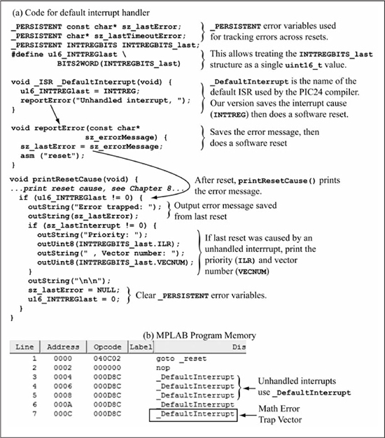
Figure 9.5(a) shows a program that tests the _DefaultInterrupt() ISR by purposefully generating a math error trap. This is done by initializing the variable u8_zero to 0, then executing u8_zero = 1/u8_zero, which generates a divide-by-zero math error trap. The u8_zero variable is declared as volatile, which means that this memory location can be modified between instruction accesses and thus disables certain compiler optimizations. If a normal variable is used, then the compiler will optimize away this seemingly useless C statement.
Figure 9.5chap09 rap_test.c: testing the _DefaultInterrupt() ISR with a math error trap
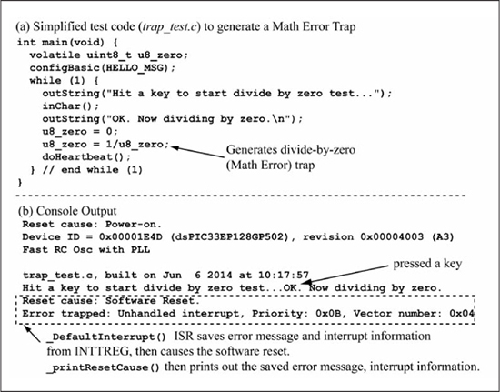
Figure 9.5(b) shows the console output generated by the code in Figure 9.5(a); observe that when a key is pressed, the while(1) loop is entered and the math error trap is generated. The priority (0x0B, 11) and vector number (0x04) output by printResetCause() match the priority in Table 9.1 and vector number in Figure 9.3.
An Example ISR
Figure 9.6(a) shows an ISR written for the math error trap; this code would be used in the source of Figure 9.5 to handle the math error trap instead of the _DefaultInterrupt() function. The function named _MathError() is used to indicate that this ISR is for the math error trap; observe that the MPLAB program memory dump in Figure 9.6(c) now shows this function address inserted in the interrupt vector table address 0x00000C that is used for the math error trap. The _MathError() code is the simplest possible ISR as all it does is clear the conditions associated with the interrupt source. In this case, the _MATHERR flag must be cleared as it is the flag that triggered the interrupt, or else the processor becomes hung in an infinite loop because each time the ISR is exited, it immediately re-enters the ISR.
Figure 9.6chap09 rap_test_handled.c: a _MathError ISR
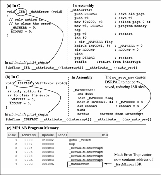
The RCOUNT register is also cleared to escape the divide repeat loop faster (the divide repeat loop would eventually be escaped but multiple divide-by-zero trap errors would be generated by the same divide instruction as the RCOUNT register is decremented each time the ISR returns to the divide instruction). Figure 9.6(a) shows the assembly code generated by the PIC24 compiler for the _MathError ISR. The _ISR macro specifies the auto_psv attribute, which instructs the compiler that the ISR function may want to access data stored in program memory through the program visibility space, so the DSRPAG register is saved on the stack and then set to a value appropriate for this ISR’s location in program memory. The _ISRFAST macro used in Figure 9.6(b) specifies the _no_auto_psv attribute, which instructs the compiler that this ISR does not use the program visibility space, so the DSRPAG register does not have to be modified. This reduces the assembly code size and reduces the latency for the ISR. The code examples use the safer _ISR macro unless speed is necessary.
Change Notification Interrupts
The first user interrupt source covered here is the input change notification interrupt, which is generated from a change of state on one or more change notification (CN) pins. Figure 9.7 shows a conceptual block diagram of the system. Each CNx input has an individual interrupt enable named CNIExy. If one or more CNIExy bits are a 1, then any state change on an enabled CNIExy input causes the change notification interrupt flag (CNIF) to be set. The weak pull-up/pull-down on each CNIExy pin can be optionally enabled, as discussed in Chapter 8.
Figure 9.7
Input change notification block diagram
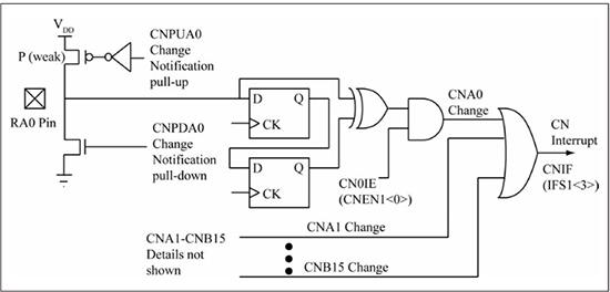
Source: Figure redrawn by author from Figure 10.6 found in the dsPIC33E/PIC24E Family Reference Manual, section 10: I/O ports (DS70000598C), Microchip Technology, Inc.
Wake from Sleep/Idle
The change notification interrupt can be used to wake the processor from sleep or idle mode. The code given in Figure 9.8 assumes the pushbutton switch PB is attached to port RB13. The config_pb() function configures RB13 as a digital input, enables the change notification pull-up (ENABLE_RB13_PULLUP()), delays to give the pull-up time to bring the pin’s voltage up to VDD, and enables the individual change notification interrupt (ENABLE_RB13_CN_INTERRUPT()). The ENABLE_RB13_CN_INTERRUPT() is a one-line macro that maps to the statement _CNIEB13 = 1. Before the while (1) loop is entered, the change notification interrupt flag is cleared, (_CNIF = 0), the change notification priority is assigned (_CNIP = 2), and the global change notification interrupt enable is set (_CNIE = 1). When enabling interrupts, it is important to clear the associated interrupt flag before the interrupt is enabled to avoid an immediate jump to the ISR. Remember that the interrupt enable does not prevent the interrupt flag from being set; it only prevents the jump to the ISR. Using priority level 2 for this interrupt is arbitrary; the only requirement is that it is greater than 0 so that the interrupt is recognized and a jump to the ISR is made when the interrupt occurs. In the while (1) loop, a message is printed then the SLEEP() macro (mapped to asm(“pwrsav #0”)) is used to put the processor to sleep. Pressing the pushbutton generates a change notification interrupt, waking the processor and causing a jump to the _CNInterrupt() ISR, which clears the change notification interrupt flag (_CNIF = 0). Upon ISR return, execution resumes in the while (1) body. Two change notification interrupts are generated for each press and release of the switch: one for the press and one for the release.
Using a Change Notification Interrupt to Measure Interrupt Latency
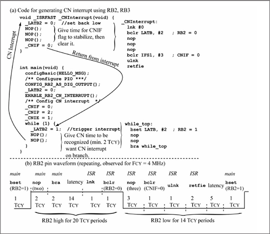
Figure 9.9(a) shows code for an experiment used to measure interrupt latency using a change notification interrupt. Pin RB2 is used as an output and an input to generate a change notification interrupt. The while (1) loop in main consists of _LATB2 = 1 to generate the interrupt; the two following nop instructions cause a two TCY period delay so that the interrupt is recognized during the bra instruction at the bottom of the loop. A change notification requires a minimum pulse width of two TCY periods to be recognized according to the datasheet [31]. The change notification interrupt causes transfer of control to the _CNInterrupt ISR, which clears RB2 (_LATB2 = 0). The three nop instructions in the ISR are used to provide delay for the change in RB2 status to propagate through the change notification logic before the CNIF flag is cleared and the ISR is exited. The ISR returns to the _LATB2 = 1 operation (bset) in the while (1) loop, causing the cycle to repeat.
Figure 9.8chap09change_wakeup.c: using the change notification interrupt to wake from sleep
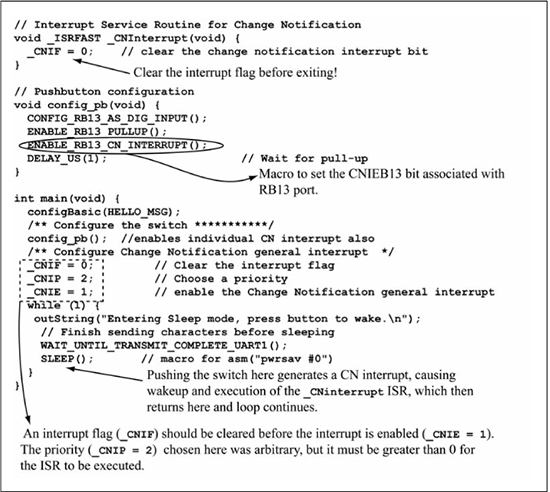
Figure 9.9(b) shows the repeating square wave on the RB2 pin caused by repeatedly bouncing between the while (1) loop and the _CNInterrupt() ISR. Both the high and low periods are eight TCY periods. This experiment was run with a slow FCY (4 MHz) so that the output port delay was small with regard to TCY; if you try this with a fast FCY such as 60 MHz you may get different results because of the variation as to where the interrupt occurs within TCY for an instruction.
Figure 9.9chap09change_latency.c: using the change notification interrupt to measure interrupt latency
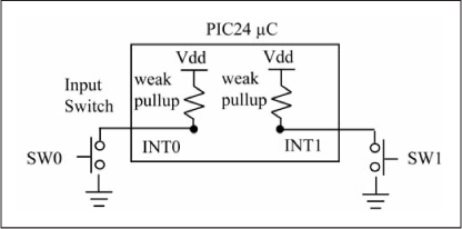
INTx External Interrupts and Remappable Pins
The INTx interrupt inputs are another interrupt source on the PIC24 μC and set their corresponding interrupt flags (INTxIF) on either a rising or falling edge transition as determined by their corresponding edge polarity select bit (INTxEP = 1 selects falling edges while INTxEP = 0 selects rising edges). Most PIC24 microcontrollers implement three INTx interrupt inputs (INT0, INT1, INT2). The PIC24 pin diagram of Figure 8.2 shows that INT0 is assigned pin 16 but that the INT1/INT2 inputs are not assigned to any pins. To expose this functionality, these pins must be mapped to an external pin. Internal pin functions such as INT1/INT2 on some PIC24 microcontrollers can be assigned to external remappable I/O pins (the RPn pins in Figure 8.2) or to external remappable input-only pins (RPIn pins in Figure 8.2), which means that special function register bits control how these internal pins are mapped to external pins. The number of RPn and RPIn pins varies by processor, and some PIC24 processors lack remappable pins altogether. Table 9.3 shows some of the remappable function inputs on the dsPIC33EP128GP502. To assign one of these input functions to an external RPn/RPIn pin, the function’s RPn/RPIn selection bits shown in column 3 are assigned the value n. The input function’s RPn/RPIn selection bits are actually multiplexor select bits that steer an RPn/RPIn input to the input function pin. After reset, these RPn/RPIn selection bits are zero, which means the input is not assigned to any RPn/RPIn pin. As an example, the following statement steers pin RP38, located on port RB6, to the INT1 input function:
_INT1R = 38; // Assign INT1 to pin RP38/RB6.
The code uses a macro to accomplish this (defined in libincludepic24_ports.h):
CONFIG_INT1_TO_RP(RB6_RP);
The value RB6_RP stands for “the remappable pin located on port RB6,” which in this case is RP38. The mapping between RP numbering and Rxy numbering varies widely across different PIC24 devices; using these values simplifies the code and allows it to work for many different processors.
In order to correctly use a remappable input, be sure to configure that pin as a digital input using CONFIG_Rxy_AS_DIG_INPUT(). For example, the complete code for mapping INT1 to RB6 is:
CONFIG_RB6_AS_DIG_INPUT();
CONFIG_INT1_TO_RP(RB6_RP);
Table 9.3: Selected Remappable Inputs for the dsPIC33EP128GP502
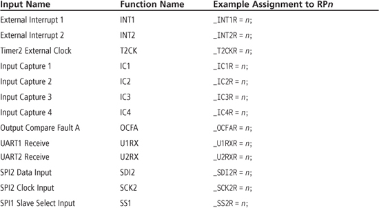
Table 9.4 shows some of the remappable output functions for the dsPIC33EP128GP502. Remappable outputs may only use RPn pins, but not the RPIn pins, because these only support remappable inputs. Each remappable pin RPn is assigned a 5-bit field named RPnR; the value of this bit field controls the output function that is mapped to it. Each RPnR bit field contains the selection bits for a multiplexor that steers an output pin function to its associated RPn pin. After reset, each RPnR bit field is zero which means that no output function assignment is made. The following statement steers the U1TX output to the RP43 pin, which is shared with RB11:
_RP43R = 1; // Assign U1TX (which is function code 1) to RP43R.
The code examples use a macro to accomplish this (defined in libincludepic24_ports.h):
CONFIG_U1TX_TO_RP(RB11_RP);
To prepare a remappable output for use, be sure to configure it as a digital output using CONFIG_Rxy_AS_DIG_OUTPUT().
The RPn configuration bits for both input and output mapping can be protected from writes by the IOLOCK bit (OSCCON<6>). At reset, IOLOCK is cleared, which allows unlimited writes to the RPn configuration bits. Setting IOLOCK prevents further writes to the RPn configuration bits. The purpose of the IOLOCK bit is to prevent accidental reconfiguration of the I/O pins, which could be disastrous in a production system. The suggested use of the IOLOCK bit is to perform all pin configuration and then set the IOLOCK bit. The code examples are intended for experimentation purposes, and thus do not change the IOLOCK from its default state of zero. Note that the __builtin_write_OSCCONL function must be used to write the OSCCON register since an unlock sequence is required when writing to this register. The IOL1WAY bit in the configuration registers (see [27]) offers an additional level of protection against reconfiguration. The default (unprogrammed) state for IOL1WAY, which corresponds to the IOL1WAY = ON setting, prevents IOLOCK from being cleared once it is set. This means that the configuration bits cannot be changed after the IOLOCK bit is set. The default configuration bits in libsrcpic24_configbits.c use the IOL1WAY = OFF setting, which allows normal setting/clearing of the IOLOCK bit.
Table 9.4: Selected Remappable Outputs for the dsPIC33EP128GP502

Returning to the subject of INT0/INT1/INT2 external interrupts, Listing 9.1 shows the code in Figure 9.8 modified to use INT1 for waking from sleep mode. Either a negative (falling) or a positive (rising) edge can be selected to wake the processor; the code uses a negative edge via the statement _INT1EP = 1. The CONFIG_INT1_TO_RP(RB13_RP) macro is used to steer the RB13 pin to the INT1 interrupt.
Listing 9.1: chap09int0_wakeup.c: Using INT1 to Wake from Sleep Mode
// Interrupt Service Routine for INT1
void _ISR _INT1Interrupt(void) {
  _INT1IF = 0;    //clear the interrupt bit
}
// Pushbutton configuration, uses RB13.
void config_pb(void) {
  CONFIG_RB13_AS_DIG_INPUT();      //use RB13 for switch input
  ENABLE_RB13_PULLUP();            //enable the pull-up
  DELAY_US(1);                     // Wait for pull-up
}
int main(void) {
  configBasic(HELLO_MSG);
  /** Configure the switch ***********/
  config_pb();
  CONFIG_INT1_TO_RP(RB13_RP);

  /** Configure INT1 interrupt  */
  _INT1IF = 0;   //Clear the interrupt flag
  _INT1IP = 2;   //Choose a priority
  _INT1EP = 1;   //negative edge triggered
  _INT1IE = 1;   //enable INT1 interrupt
  while (1) {
   outString(“Entering Sleep mode, press button to wake.
”);
   //finish sending characters before sleeping
   WAIT_UNTIL_TRANSMIT_COMPLETE_UART1();
   SLEEP();       //macro for asm(“pwrsav #0”)
  }
}
Switch Inputs and Change Notification/INTx Interrupts
It is tempting to use either the change notification or INTx interrupts for processing switch input events. However, writing code to correctly handle the multiple interrupt flag events caused by mechanical switch bounce is problematic. Timers provide an interrupt-centric way to wait until switch bounce ceases, then trigger an interrupt to update the state in a state machine. The change notification and INTx interrupts can only be directly applied to signal sources that have clean transitions, such as those produced by an external integrated circuit.
Periodic Timer Interrupts
Other user interrupt sources available on the PIC24 include various timer interrupts. Recall from Chapter 8 that a timer is simply a counter, with elapsed time computed as shown in Equation 9.2, where TTMR is the timer clock period and Ticks is the number of elapsed timer counts.
There are multiple timers available on the PIC24, some of which are special-purpose timers such as the watchdog and power-on reset timers while others are general-purpose such as Timers 1 through 5. This chapter discusses the use of Timer2 and Timer3 for generating periodic interrupts, with full coverage of timers reserved for Chapter 12.
Timer2 and Timer3 are two general-purpose timers that can either act as separate 16-bit timers or be combined into one 32-bit timer named Timer2/3. Other PIC24 family members have additional paired timers numbered Timer4/5, Timer 6/7, and so on; these paired timers have the same functionality as Timer2/3. From the Timer2 block diagram of Figure 9.10, note that the timer can be clocked by either an external clock on the T2CK pin or from the internal clock (TCY). The prescaler for the Timer2 clock has four settings of 1:1, 1:8, 1:64, and 1:256. This chapter’s applications always uses the internal clock source (TGATE = 0, TCS = 0). In this mode, the Timer2 interrupt flag (T2IF) is set whenever the Timer2 register (TMR2) contents are equal to the Timer2 period register (PR2) contents, which also resets TMR2 to 0. Note: The diagram in Figure 9.10 comes from the older but clearer PIC24H datasheets; see Figure 11.2 of [19].
Figure 9.10
Timer2 block diagram

Source: Figure redrawn by author from Figure 11.2 found in the PIC24H32GP202 datasheet (DS70289B), Microchip Technology, Inc.
The time between TMR2 resets is known as the Timer2 timeout period (TT2IF) and is calculated as shown in Equation 9.3 (recall that TCY is equal to 1/FCY):
Table 9.5 shows minimum and maximum TT2IF periods for FCY = 60 MHz. The minimum timeout period is also the timer accuracy, which decreases with larger prescaler values. The 32-bit Timer2/3 mode is useful for longer timeout periods.
Table 9.5: Timer2 Min/Max Timeouts for FCY = 60 MHz
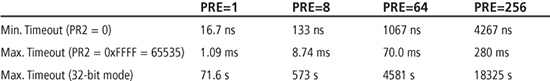
Figure 9.11 gives detailed information on the Timer2 configuration (T2CON) register that contains the control bits shown in Figure 9.10. This chapter uses the internal clock and 16-bit mode for Timer2, which means bit settings of T32 = 0, TCS = 0, and TGATE = 0 (timers are discussed further in Chapter 12). The Timer3 block diagram is the same as Timer2, with TMR2, PR2, T2IF, and T2CK replaced by TMR3, PR3, T3IF, and T3CK. The T3CON register is the Timer3 configuration register and has the same control bits as T2CON except for the T32 bit.
Figure 9.11
T2CON register details

Source: Figure redrawn by author from Register 11.1 found in the dsPIC33/PIC24 FRM section 11: timers (DS70362B), Microchip Technology, Inc.
This chapter uses Timer2 and Timer3 to generate periodic interrupts based on the T2IF or T3IF flags. A periodic interrupt is useful for sampling inputs at some desired periodic interval. Because Equation 9.3 has two variables (PR2 and PRE), there may be more than one solution for the desired interrupt period. One approach for determining PR2, PRE is to select a PRE (prescale) value, then solve for the PR2 value that gives the desired period, as shown in Equation 9.4:
Table 9.6 shows calculated PR2 values for each possible prescaler value, assuming a desired period interrupt of 15 ms and FCY = 60 MHz. The PR2 values for PRE = 1 and PRE = 8 cannot be used since they are greater than 65535 (recall that PR2 is a 16-bit register). If accuracy is important for the periodic interrupt, then the lowest prescaler value should be used. The values in Table 9.6 are rounded to the nearest integer value.
Table 9.6: PR2/PRE Values for TT2IF = 15 ms, FCY = 60 MHz
Timer Macros and Support Functions
Listing 9.2 shows the Timer2 macros contained in libincludepic24_timer.h. Similar macros are defined for higher-numbered timers, and are compatible with the PIC24/dsPIC33 F, H, and E families.
/* T2CON: TIMER2 CONTROL REGISTER */
#define T2_ON               0x8000       /* Timer2 ON */
#define T2_OFF              0x0000       /* Timer2 OFF */
#define T2_OFF_ON_MASK     (~T2_ON)

#define T2_IDLE_STOP        0x2000 /* stop operation during sleep */
#define T2_IDLE_CON         0x0000 /* operate during sleep */
#define T2_IDLE_MASK        (~T2_IDLE_STOP)

#define T2_GATE_ON          0x0040 /* Timer Gate time accumulation enabled */
#define T2_GATE_OFF         0x0000 /* Timer Gate time accumulation disabled */
#define T2_GATE_MASK        (~T2_GATE_ON)

#define T2_PS_1_1           0x0000       /* Prescaler 1:1  */
#define T2_PS_1_8           0x0010       /*            1:8 */
#define T2_PS_1_64          0x0020       /*           1:64 */
#define T2_PS_1_256         0x0030       /*          1:256 */

#define T2_PS_MASK           (~T2_PS_1_256)

#define T2_32BIT_MODE_ON    0x0008      /* Timer2 and Timer3 form a 32 bit Timer */
#define T2_32BIT_MODE_OFF   0x0000
#define T2_32BIT_MODE_MASK  (~T2_32BIT_MODE_ON)

#define T2_SOURCE_EXT       0x0002 /* External clock source */
#define T2_SOURCE_INT       0x0000 /* Internal clock source */
#define T2_SOURCE_MASK      (~T2_SOURCE_EXT)
The macros of Listing 9.2 can be used to set the T2CON register contents in a self-documenting manner, such as the following:
T2CON = T2_OFF | T2_IDLE_CON | T2_GATE_OFF | T2_32BIT_MODE_OFF
        | T2_SOURCE_INT | T2_PS_1_64;  // Results in T2CON=0x0020.
This is clearer to an external reader than writing T2CON = 0x0020 and so the code examples use this style for timer configuration. The following line of code shows how to use a mask macro to modify a bit field without disturbing the other bits in the register:
T2CON = (T2CON & T2_PS_MASK) | T2_PS_1_8;
There are no individual bit macros such as _TON defined for the timer configuration registers because the bit names are the same for the different timer registers. However, in addition to the mask macros, you can also use the C structure references (see Chapter 8) to change bits in the timer registers, as shown in the following code line:
T2CONbits.TON = 1; // Turn on timer2.
The file libsrcpic24_timer.c contains timer support functions as shown in Listing 9.3. The msToU16Ticks(uint16_t u16_ms, uint16_t u16_pre) function is based on Equation 9.3 and converts milliseconds (u16_ms parameter) to timer ticks given the timer prescale value (u16_pre parameter) and the predefined FCY macro. The usToU16Ticks() function is similar except it converts microseconds to timer ticks. Floating point computation is used internally in the timer ticks conversion functions to accommodate a wide range of FCY and timer prescale values. Because of this, it is recommended that you avoid using these functions in time-critical code sections. Calls to the ASSERT() function implement range checking within msToU16Ticks() and usToU16Ticks() to verify that the requested timeout period can fit in the uint16_t return value given the timer prescale and FCY values. If the calculation overflows the 16-bit range, then the reportError() function is called that saves an error message and executes a software reset. The error message is output to the serial console when printResetCause() is called by main(). The getTimerPrescale(TxCONbits) macro calls the getTimerPrescaleBits(uint8_t u8_TCKPS) function, which returns the timer prescale value given a timer configuration register.
Listing 9.3: Timer Support Functions
// Convert milliseconds to Timer ticks.
uint16_t msToU16Ticks(uint16_t u16_ms, uint16_t u16_pre) {
  float f_ticks = FCY;
  uint16_t u16_ticks;
  f_ticks = (f_ticks*u16_ms)/u16_pre/1E3;
  ASSERT(f_ticks < 65535.5);
  u16_ticks = roundFloatToUint16(f_ticks);  //back to integer
  return u16_ticks;
}
// Convert microseconds to Timer ticks.
uint16_t usToU16Ticks(uint16_t u16_us, uint16_t u16_pre) {
  float f_ticks = FCY;
  uint16_t u16_ticks;
  f_ticks = (f_ticks*u16_us)/u16_pre/1E6;
  ASSERT(f_ticks < 65535.5);
  u16_ticks = roundFloatToUint16(f_ticks);  //back to integer
  return u16_ticks;
}
// Return the timer prescale based on the TxCONbits SFR.
#define getTimerPrescale(TxCONbits) getTimerPrescaleBits(TxCONbits.TCKPS)
// Return the timer prescale based on the TCKPS bitfield in TxCONbits.
uint16_t getTimerPrescaleBits(uint8_t u8_TCKPS) {
  const uint16_t au16_prescaleValue[] = { 1, 8, 64, 256 };
  ASSERT(u8_TCKPS <= 3);
  return au16_prescaleValue[u8_TCKPS];
}
The functions of Listing 9.3 are useful for setting the PR2 register to a particular timeout value, as shown in the following code line that configures PR2 to a timeout value equivalent to 15 ms.
PR2 = msToU16Ticks(15, getTimerPrescale(T2CONbits)) - 1;
The value returned by msToU16Ticks() is decremented by one because the Timer2 period is PR2 + 1.
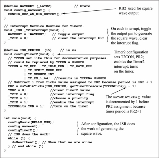
Square Wave Generation
A simple test of the Timer2 periodic interrupt capability is shown in Figure 9.12 that generates a square wave on the RB2 pin. The configTimer2() function configures Timer2 for 16-bit mode with a prescale value of 64, sets the PR2 timeout to 15 ms, and enables the Timer2 interrupt. The _T2Interrupt ISR toggles the RB2 pin on each interrupt and clears the T2IF flag before returning. After main() configures RB2 and Timer2, the while (1) loop only has the doHeartbeat() call because the ISR does all of the work of generating the square wave. This is not the best way to generate a square wave and is only intended as an illustration of a periodic interrupt; Chapter 12 discusses other methods for waveform generation.
Figure 9.12chap09squarewave.c: square wave generation using Timer2
Listing 9.4 shows the changes to Figure 9.12 for using Timer3 instead of Timer2. The configTimer3() function ensures 16-bit mode is selected via the statement T2CONbits.T32 = 0 before configuring the T3CON register, which does not have the T32 control bit. The ISR is the same as Figure 9.13 except for function name (_T3Interrupt) and interrupt flag (_T3IF).
void _ISR _T3Interrupt(void) {
  WAVEOUT = !WAVEOUT;          //sample the switch
  _T3IF = 0;                     //clear the timer interrupt bit
}
void configTimer3(void) {
  // Ensure that Timer2/3 are configured as separate timers.
  T2CONbits.T32 = 0;     // 32-bit mode off
  // T3CON set like this for documentation purposes.
  // Could be replaced by T3CON = 0x0020.
  T3CON = T3_OFF | T3_IDLE_CON | T3_GATE_OFF
           | T3_SOURCE_INT
           | T3_PS_1_64;
  PR3 = msToU16Ticks(ISR_PERIOD, getTimerPrescale(T3CONbits)) - 1;
  TMR3  = 0;                   // Clear timer3 value
  _T3IF = 0;                   // Clear interrupt flag
  _T3IP = 1;                   // Choose a priority
  _T3IE = 1;                   // Enable the interrupt
  T3CONbits.TON = 1;           // Turn on the timer
}
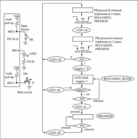
Interrupt-Driven LED/Switch I/O
The LED/switch I/O problem of Chapter 8 is repeated here in Figure 9.13. Recall that the original code solution used polling for the switch within the while (1) loop and two states for each of the press and release actions. The following two approaches demonstrate a more efficient solution to this problem by making use of interrupts to reduce CPU cycles (and use less power) by avoiding polling.
Input Sampling
One standard usage of periodic interrupts is for input sampling. The code in chap09ledsw1_sampling.c began with the LED/switch toggle example of Figure 8.24, but was modified to use the Timer3 periodic interrupt for sampling the pushbutton input, which then runs the FSM based on this sampled value:
void _ISR _T3Interrupt(void) {
  _T3IF = 0;
  update_state();
}
Figure 9.13
State machine specification for LED/switch I/O problem

The Timer3 configuration is the same as Listing 9.4 and is not shown. For this approach, the LED blinking action should not be done in the ISR as this involves placing a software delay in the ISR, which violates the principle that an ISR should do its work as quickly as possible. A software delay consists of wasted cycles, and an ISR should not be wasting cycles! Instead, the FSM run in the ISR sets u16_doBlink to request blinking, then clears it before exiting the current state:
volatile uint16_t u16_doBlink = 0;
void update_state(void) {
  ... some states omitted ...
    case STATE_RELEASED3_BLINK:
      // Toggle the LED.
      u16_doBlink = 1;

      if (u16_led_toggles >= 10) {
        e_state = STATE_RELEASED1;
        // Stop toggling
        u16_doBlink = 0;
      }
      if (PB_PRESSED()) {
        e_state = STATE_PRESSED3;
        // Stop toggling
        u16_doBlink = 0;
      }
      break;
Other than adding two conditional assignments to the RELEASED3_BLINK state, the remainder of the FSM is identical to the FSM given in the previous chapter. To actually perform the blinking, the main() code only monitors the semaphore state and performs the desired blinking:
int main(void) {
  ... configuration code not shown ...

  while (1) {
    if (u16_doBlink) {
      u16_led_toggles++;
      DELAY_MS(250);
      LED1 = !LED1;
      printf(“toggles = %d
”, u16_led_toggles);
    }
    doHeartbeat();
   }
}
Observe that the volatile modifier is used in the u16_doBlink variable declaration. This notifies the compiler that this can be modified by an external agent (e.g., an ISR) between successive accesses (reads) in the main() code and prevents certain compiler optimizations from being applied. The volatile modifier should be used with any variable modified by an ISR and accessed outside of the ISR.
The variable u16_doBlink is a semaphore, which is a flag set by an ISR to signal the foreground task that an I/O action has occurred. Generally, the ISR sets the semaphore indicating that an I/O action has been processed and is ready. The foreground task detects that the semaphore is set, reads the I/O event result and resets the semaphore, thus indicating to the ISR that the I/O event has been consumed. An advantage of using the foreground task to clear the semaphore is that the ISR can determine if the foreground task is processing interrupts fast enough to keep pace with I/O event occurrence. If the semaphore is still set when the ISR receives an I/O event then the foreground task is processing I/O events too slowly, and some sort of event buffering may be needed (as covered in Chapter 10).
How long should the ISR period be in order to debounce a human-activated pushbutton switch? Figure 9.14 shows a low-true bouncy switch being sampled by a periodic interrupt, with bounce occurring on both switch press and release. The bounce times are labeled as TBNCE1 and TBNCE2 (generically referred to as TBNCE) and are assumed to be approximately equal to each other. For the high-to-low transition of a switch press, if the ISR samples at a high bounce point, then the ISR period must be short enough so that the next sample sees the switch activation or else the activation is missed. If the ISR samples at a low bounce point, then the ISR period must be long enough for the bounces to settle or else the next sample may be at a high bounce point, causing the ISR to see a false switch release. This means the ISR period must be greater than the bounce time (TBNCE) and less than half the expected pulse width (TPW/2) to guarantee two samples per switch activation. For human-activated switches, the pulse width (TPW) is greater than 100 ms based on human reaction times. The bounce time (TBNCE) depends on the switch, but is generally less than 5 ms. An ISR period of 15 ms works well if you want to guarantee multiple samplings of a human-activated pushbutton. Having the sampling period greater than the bounce time means that for the low-to-high transition of a switch release, only one sample is possible during the TBNCE2 period. If the ISR samples low during TBNCE2, the next sample is a high value, generating a clean switch release event. If the ISR samples high during TBNCE2, a clean switch release event is seen because the next sample is also high.
Change Notification with a Timer
A second approach further increases efficiency and responsiveness by only running the CPU when a button is pressed or released, rather than running it periodically to sample an input. This method employs a change notification interrupt to detect a pushbutton press or release. In order to avoid problems with switch bounce, the state machine will be run after a debounce delay after the pushbutton triggers a change notification interrupt; Timer3 will be used to provide this delay. Inside the state machine, the inefficient DELAY_MS statement used in the previous chapter for blinking the LED will likewise be replaced with a Timer3 interrupt.
Figure 9.14
Switch bounce and interrupt period

This section begins by examining the change notification ISR, which disables itself to avoid switch bounce, then arms the timer to update the FSM state after a debounce delay.
void _ISR _CNInterrupt(void) {
  // Acknowledge the interrupt, then disable it. Otherwise, any switch bounce
  // would cause spurious interrupts.
  _CNIF = 0;
  _CNIE = 0;
  // Schedule a timer interrupt after a debounce delay.
  timer3_arm(DEBOUNCE_DLY);
}
The timer3_arm() routine provides a convenient method for scheduling a Timer3 interrupt u16_time_ms in the future:
void timer3_arm(uint16_t u16_time_ms) {
  // If a timer interrupt has occurred but has not been processed,
  // discard it and rearm.
  _T3IF = 0;

  // Convert arm time to Timer3 ticks.
  PR3 = msToU16Ticks(u16_time_ms, getTimerPrescale(T3CONbits)) - 1;
  TMR3 = 0;
  T3CONbits.TON = 1;
}
After a DEBOUNCE_DLY of 15 ms, the timer interrupt occurs. The effects of switch bounce on the disabled change notification interrupt can be cleared, the change notification interrupt re-enabled, and the FSM run.
void _ISR _T3Interrupt(void) {
  // Clear the interrupt flag.
  _T3IF = 0;
  // Stop the timer; the debounce delay is done.
  T3CONbits.TON = 0;
  // Clear the change notification interrupt because switch bounce
  // may have set it.
  _CNIF = 0;
  // Re-enable change notification interrupts, since the debounce
  // delay is done.
  _CNIE = 1;
  // Run our state machine.
  update_state();
}
The state machine in update_state() is almost identical to the code given in Chapter 8. Two changes must be made in order to replace the inefficient DELAY_MS call with a timer interrupt. First, a timer interrupt must be scheduled when leaving the PRESSED2 state; there are otherwise no interrupt sources (such as pushbutton presses producing a change notification interrupt or timer interrupts scheduled), which will run the code in the RELEASED3_BLINK state. The changes made inside switch (e_state) are shown in Figure 9.15.
One significant benefit of this approach is efficiency: CPU cycles are used to process switch and timer interrupts, rather than idly poll a pushbutton or spend millions of CPU cycles delaying for a fixed amount of time. This is most clearly seen in the following main() routine; when done with its work, the PIC24 enters the idle state to save power. For additional savings, Timer3 can be run from an external clock source, allowing the PIC24 to sleep.
int main(void) {
  configBasic(HELLO_MSG);
  config_pb();
  config_sw();
  CONFIG_LED1();

  configTimer3();
  config_cn();

  while (1) {
   IDLE();
  }
}
Unfortunately, this approach has one significant drawback: though it implements the state machine shown in Figure 9.13, its operation differs markedly from the polling and the periodic sampling approach. The differences are apparent when the next state is run. When polling or performing periodic sampling, the next state is run immediately (polling) or in 15 ms (sampling), so that the actions of the next state (turning an LED on, for example) occur almost immediately. In contrast, in this approach the next state is run only when the next event occurs. For example, a button press changes the state assignment, but does not then perform the assignment in that next state until the next button press, which occurs an indeterminate amount of time later.
Figure 9.15chap09ledsw1_cn.c: Changes made to update_state() from Chapter 8 for interrupt-driven operation
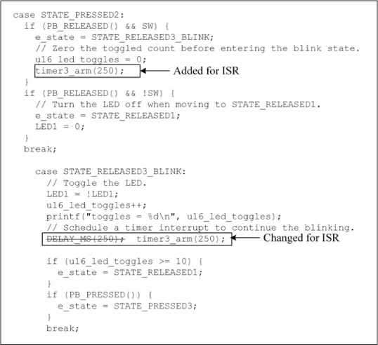
To achieve results that match the polling and period sampling approaches, a different state machine must be designed, which relies on conditional state assignments to turn the LED on and off when an event occurs, rather than waiting until the next state to do so. In particular, all unconditional state outputs must be placed as a conditional state output in all states which transition to a state with an unconditional state output. For example, consider state LED_OFF, where the unconditional assignment LED1 = 0 is made. This state can be reached from state PRESSED2 when SW == 0, state RELEASED3_BLINK when toggles >= 10, or from state PRESSED3 when PB is pressed. Therefore, the single assignment LED1 = 0 must be placed in all three of these state transitions. Likewise, the unconditional assignment LED1 = 1 in state RELEASED2 must become a conditional assignment when transitioning from PRESSED1 to RELEASED2, and LED1 = 1 in state PRESSED3 becomes a conditional assignment when transitioning from RELEASED3_BLINK to PRESSED3.
The revised state machine and resulting code for update_state() is given in Figure 9.16 and Listing 9.5; these illustrate the preferred method when using this approach. Using this revised state machine, all three approaches (Chapter 8’s polling, the previous section’s input sampling, and this revised approach) now produce identical results.
Listing 9.5: chap09ledsw1_cn_revised.c: Revised update_state() for Change Notification with Timers; Changes Shown in Bold Type
void update_state(void) {
  static state_t e_state = STATE_RELEASED1;
  // The number of times the LED was toggled in the blink state
  static uint16_t u16_led_toggles;

  switch (e_state) {
  case STATE_RELEASED1:
    if (PB_PRESSED()) {
      e_state = STATE_PRESSED1;
    }
    break;

    case STATE_PRESSED1:
      if (PB_RELEASED()) {
        e_state = STATE_RELEASED2;
        // Turn the LED on when entering STATE_RELEASED2.
        LED1 = 1;
      }
      break;

    case STATE_RELEASED2:
      if (PB_PRESSED()) {
Figure 9.16
Revised FSM for change notification with a timer approach
    e_state = STATE_PRESSED2;
    }
    break;

case STATE_PRESSED2:
  if (PB_RELEASED() && SW) {
    e_state = STATE_RELEASED3_BLINK;
    // Zero the toggled count before entering the blink state.
    u16_led_toggles = 0;
    // Schedule a timer interrupt to start the blinking.
    timer3_arm(250);
  }
  if (PB_RELEASED() && !SW) {
    e_state = STATE_RELEASED1;
    // Turn the LED off when moving to STATE_RELEASED1.
    LED1 = 0;
  }
  break;

case STATE_RELEASED3_BLINK:
  // Toggle the LED.
  LED1 = !LED1;
  u16_led_toggles++;
  printf(“toggles = %d
”, u16_led_toggles);
  // Schedule a timer interrupt to continue the blinking.
  timer3_arm(250);

  if (u16_led_toggles >= 10) {
    e_state = STATE_RELEASED1;
    // Turn the LED off when moving to STATE_RELEASED1.
    LED1 = 0;
  }
  if (PB_PRESSED()) {
    e_state = STATE_PRESSED3;
    // Freeze the LED on when exiting the blink state.
    LED1 = 1;
  }
  break;

case STATE_PRESSED3:
  if (PB_RELEASED()) {
    e_state = STATE_RELEASED1;

        // Turn the LED off when moving to STATE_RELEASED1.
        LED1 = 0;
      }
      break;

    default:
      ASSERT(0);
  }
  print_state(e_state);
}
Filtering Noisy Inputs
A common problem in microcontroller interfacing is sampling a noisy input that may have false glitches in the signal. This is a different problem than switch debouncing because the glitches can occur anywhere in the signal, unlike switch noise that occurs for a short time period after the switch changes state. This means that the periodic sampling approach alone will not guarantee correct interpretation of noisy inputs. The Schmitt Trigger (Chapter 8) input buffer on each PIO coupled with an external low-pass RC filter can provide a good solution for sampling noisy inputs. A low-pass RC filter as shown in Figure 9.17(a) has a cutoff frequency of 1/(2πRC), which means that signals at this frequency are attenuated by approximately 50 percent, with attenuation increasing with frequency. To completely block a signal at a particular frequency f, use a filter with a cutoff frequency of approximately f/10. The RC filter greatly increases the rise and fall time of the port’s input signal, but the port’s Schmitt Trigger internally transforms this slowly rising or falling signal to a clean signal transition.
Figure 9.17
Noisy input filtering
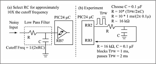
Figure 9.17(b) shows an experiment with RB2 supplying a square wave with pulse widths of TPW as an input signal to pin RB3. The goal of the experiment is to monitor the RB3 input state and determine RC values that either block or pass the signal transitions. Figure 9.18 shows the code that implements the experiment of Figure 9.17(b). The while (1) loop in main generates a square wave on TOUT (RB2) using software delays with high and low pulse widths of TPW. If the old input value (u8_oldvalueTIN) does not match the current RB3 input value (TIN), then * is printed and the current value is saved to u8_oldvalueTIN. Experimentation showed that values of R = 16 kΩ and C = 0.1 μF blocked pulse widths of 1 ms and passed pulse widths of 2 ms (your results may vary!). Because the source impedance of a noise source can affect the filter cutoff frequency, you should verify experimentally any external filtering circuitry by using an oscilloscope to monitor the filter output to observe its effect on the noisy input signal.
Figure 9.18chap09filter_test.c: RC low-pass filter experiment code

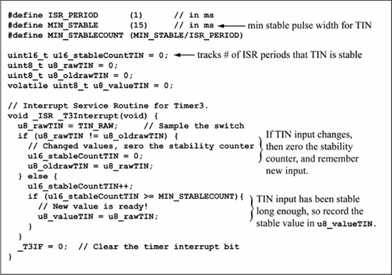
For long pulse width transients (pulse widths of multiple milliseconds), a low-pass RC filter may reduce the signal rise/fall times to unacceptably long times. In this case, a low-pass RC filter for higher frequency transients (pulse widths < 1 ms) combined with a software noise filter may be the best approach. Figure 9.19 shows the ISR for a periodic timer interrupt that is used to sample the TIN input of Figure 9.18. The ISR code includes a software glitch filter that only passes changes in the TIN input if the TIN input is stable for MIN_STABLE number of milliseconds. The u16_stableCountTIN variable is used by the ISR to track the number of successive interrupts that TIN is stable. When this counter exceeds MIN_STABLECOUNT, which is defined as MIN_STABLE/ISR_PERIOD, then the TIN value is copied to the u8_valueTIN variable used by main. Generally, the sampling period for a software glitch filter should be fast enough to achieve at least four samples for the minimum pulse width. It is not desirable to use a software filter for short pulse width transients (< 1 ms) because the ISR period becomes fairly small, requiring a larger percentage of the processor execution time.
Figure 9.19chap09sofilt_test.c: software glitch filter
A Rotary Encoder Interface
A rotary encoder is used to encode the direction and distance of a mechanical shaft’s rotation. There are different ways to accomplish this; Figure 9.20 shows a 2-bit Gray code rotary encoder. Counterclockwise rotation (a) of the shaft produces the sequence 00, 01, 11, and 10, while clockwise rotation (b) generates 00, 10, 11, and 01. In a Gray code, adjacent encodings differ by only one bit position. Rotation direction is determined by comparing the current 2-bit value with the last value.
For example, if the current value is 11 and the last value is 10, the shaft is rotating in a clockwise (b) direction. One common use for a rotary encoder is as an input device on a control panel where clockwise rotation increments a selected parameter setting, while counterclockwise rotation decrements the parameter. The rotary encoder of Figure 9.20 is an incremental encoder as the shaft’s absolute position is indeterminate; only relative motion is encoded. Some rotary encoders include more bits that provide absolute shaft position, in BCD or binary encoding. An n-position encoder outputs n codes for each complete shaft rotation. Common values of n for 2-bit incremental rotary encoders are 16 and 32. However, high-precision encoders can supply hundreds of pulses per shaft rotation.
Figure 9.20
Two-bit Gray code rotary encoder
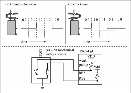
Rotary encoders use mechanical, optical, or magnetic means of detecting shaft rotation, with mechanical encoders being the least expensive and magnetic the most expensive. A key specification for optical and mechanical encoders is rotational life, with optical ~ 1 million and mechanical ~ 100,000 rotations due to mechanical wear. Magnetic encoders are meant for high-speed rotational applications with encoder lifetime measured in thousands of hours for a fixed rotational speed in revolutions per minute (RPMs). A two-bit mechanical Gray code rotary encoder, as shown in Figure 9.20(c), generally has three pins as shown, two outputs for the switches and the third output for a common ground.
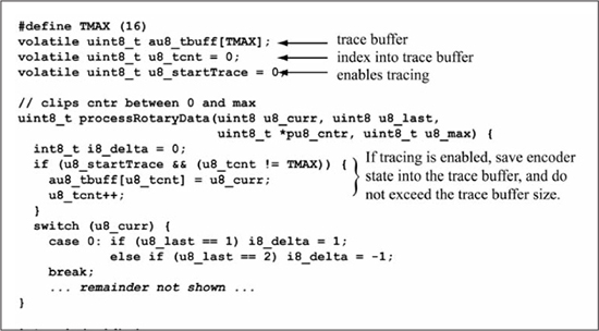
Figure 9.21 shows a utility function named processRotaryData() that is called to process a change in state for a 2-bit Gray code rotary encoder. The u8_curr and u8_last parameters are the current and last state values, respectively, of the encoder and are limited to values of 0, 1, 2, and 3. The *pi8_cntr parameter is a pointer to a counter that may either be incremented or decremented by one, depending upon the state change of the encoder. The function limits the counter value to between 0 and u8_max, as most counter variables associated with rotary encoder inputs have some sort of limit associated with them. In this implementation, modifications to the counter variable are halted when a limit is reached until the encoder rotation is reversed. An alternative implementation could wrap the counter after reaching a limit. If the function detects an illegal state change, perhaps caused by switch bounce or noise, then a non-zero value is returned from the function. Observe that the u8_delta value assigned in each case is based on the current and last states. For example, for a current state (u8_curr) of 0, a previous state (u8_last) of 1 from Figure 9.20 means that the encoder shaft has rotated clockwise, so the counter should be incremented by 1 (u8_delta = 1).
Figure 9.21chap09
ot_enc.c: the processRotaryData() utility function
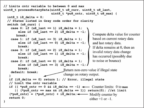
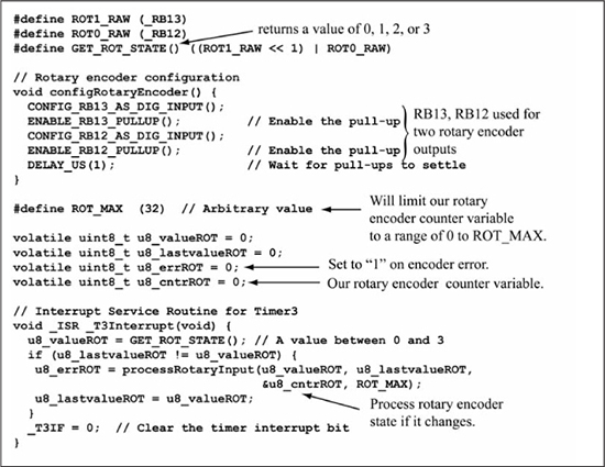
Figure 9.22 shows the ISR and main() code that reads a 2-bit Gray code rotary encoder connected to RB13 and RB12, which is periodically sampled by a 15 ms Timer3 interrupt. Because rotary encoder output is generated by switch opens and closures, the periodic sampling of the rotary encoder state handles the switch bounce. The processRotaryData() function is called by the Timer3 ISR whenever the encoder state changes, and the u8_cntrROT variable implements the rotary encoder counter variable, which is limited to a maximum value defined by ROT_MAX. The u8_errROT variable is used to hold the return value of processRotaryData() function, which is a non-zero value if an illegal state change is detected.
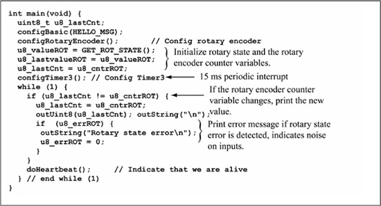
The main() configuration code in Figure 9.22 uses the configRotaryEncoder() function to configure RB13/RB12 as inputs with weak pull-ups for the two rotary encoder outputs. The 1 μs software delay that follows is needed to give time for the weak pull-ups on the inputs to stabilize, so that the u8_valueROT variable that contains the initial state of the rotary encoder is initialized to a stable value. The while (1) loop prints the u8_cntrROT value any time a change is detected and also prints an error message if the u8_errROT variable becomes non-zero.
Figure 9.22chap09
ot_enc.c: a 2-bit Gray code rotary encoder interface example
A Keypad Interface
A numeric keypad is a common element in a microcontroller system, as it provides an inexpensive method of input. A numeric keypad is simply a matrix of switches arranged in rows and columns and has no active electronics; a keypress connects a row and column pin together, as shown in Figure 9.23.
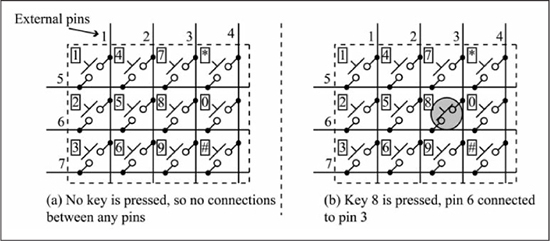
The 4x3 numeric keypad of Figure 9.23 is shown connected to the PIC24 μC in Figure 9.24. The RB[5:3] port pins are configured as outputs driving low and connected to the row pins, while RB[9:6] are configured as inputs with the weak pull-ups enabled and connected to the column pins.
Figure 9.24
4x3 numeric keypad connected to the PIC24 μC
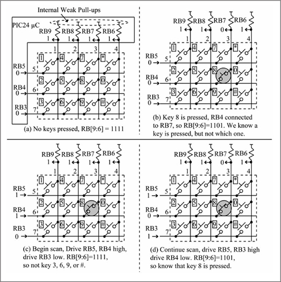
If no key is pressed as in Figure 9.24(a), RB[9:6] reads as 1111 because there are no connections to the RB[5:3] pins. In Figure 9.24(b), key 8 is pressed, connecting RB7 to RB4, causing RB7 to become a 0.
The keypress can be detected by any of the mechanisms previously discussed, such as polling, periodic sampling via a timer interrupt, or using the change notification inputs associated with the PORTB pins.
After a keypress is detected, determining which key is actually pressed is done through a procedure known as a keypad scan. The keypad scan first determines which column input is low. Then it steps through the rows, driving the one row low and the remaining rows high. If the column input originally found as low remains low, then the corresponding row for the keypress has been discovered. This scan procedure only detects one key when multiple keys are pressed, but it is straightforward to modify it to detect multiple keypresses. In Figure 9.24(b), a keypress is detected when the RB7 column input is read as low. The scan is started in Figure 9.24(c) by driving RB3 low and RB4 and RB5 high. The RB7 column input remains high, so key 9 is not pressed. In Figure 9.24(d), RB4 is driven low and RB3 and RB5 high. At this point, the RB7 column input is found to be low, indicating that key 8 is pressed creating the connection between RB4 and RB7.
Listing 9.6 shows some interface macros and support functions for the keypad interface. Macros C0, C1, C2, and C3 are four column input states, with macros R0, R1, and R2 for the row states. The configKeypad() function configures the column inputs with pull-ups enabled and the rows as outputs all driving low. The remaining functions are self-explanatory.
Listing 9.6: chap09keypad.c: Interface Macros, Support Functions for Keypad Interface
#define C0 (_RB9)
#define C1 (_RB8)
#define C2 (_RB7)
#define C3 (_RB6)

void config_column(void) {
  CONFIG_RB9_AS_DIG_INPUT(); ENABLE_RB9_PULLUP();
  CONFIG_RB8_AS_DIG_INPUT(); ENABLE_RB8_PULLUP();
  CONFIG_RB7_AS_DIG_INPUT(); ENABLE_RB7_PULLUP();
  CONFIG_RB6_AS_DIG_INPUT(); ENABLE_RB6_PULLUP();
}

#define R0 (_LATB5)
#define R1 (_LATB4)
#define R2 (_LATB3)

#define CONFIG_R0_DIG_OUTPUT() CONFIG_RB5_AS_DIG_OUTPUT()
#define CONFIG_R1_DIG_OUTPUT() CONFIG_RB4_AS_DIG_OUTPUT()
#define CONFIG_R2_DIG_OUTPUT() CONFIG_RB3_AS_DIG_OUTPUT()

void config_row(void) {
  CONFIG_R0_DIG_OUTPUT();
  CONFIG_R1_DIG_OUTPUT();
  CONFIG_R2_DIG_OUTPUT();
}

void drive_row_low(void) {
  R0 = 0; R1 = 0; R2 = 0;
}

void drive_row_high(void) {
  R0 = 1; R1 = 1; R2 = 1;
}

void configKeypad(void) {
  config_row();
  drive_row_low();
  config_column();
  DELAY_US(1);     //wait for pull-ups to stabilize inputs
}
Figure 9.25 shows the doKeyScan() function for the keypad interface, which first identifies the column input that is low, storing it in the u8_col variable. The function then scans the keypad as previously described using a for loop with loop variable u8_row. Within the loop, the u8_setOneRowLow(u8_row) function call drives the row specified by u8_row as low and the remaining rows high. When a column input is detected low during the loop, the variables u8_row and u8_col are used to access the two-dimensional array au8_keyTable to return the ASCII value of the pressed key. An “E” character is returned if the key scan finds no column input that is low, indicating that no character is available. The KEY_PRESSED() macro returns true if any column is low, while the KEY_RELEASED() macro is true if all columns are high.
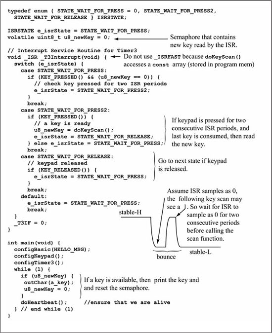
Figure 9.26 shows the ISR and the main() code for the keypad interface. The ISR uses a three-state FSM to detect presses and releases on the keypad. If a key is pressed for two consecutive ISR periods and the last key value has been consumed, then the keypad is scanned using the doKeyScan() function. The reason for waiting two consecutive ISR periods for the keypress is that in the previous switch sampling examples, you were guaranteed that switch samples were separated by an ISR sampling period. However, in this case the doKeyScan() function resamples the switch after the ISR has detected it as low. The doKeyScan() function will thus be sampling during the bounce period, so it could see a 1 instead of a 0. Waiting for the ISR to sample a 0 for two consecutive periods means that the doKeyScan() function will read the key during the stable-L period of Figure 9.14. The new key value is returned in u8_newKey, which functions as a semaphore when its value is non-zero. The while (1) loop in main() waits for a non-zero value in u8_newKey, prints the key value to the screen, and then clears u8_newKey.
Figure 9.25chap09keypad.c: the doKeyScan() function for the keypad interface
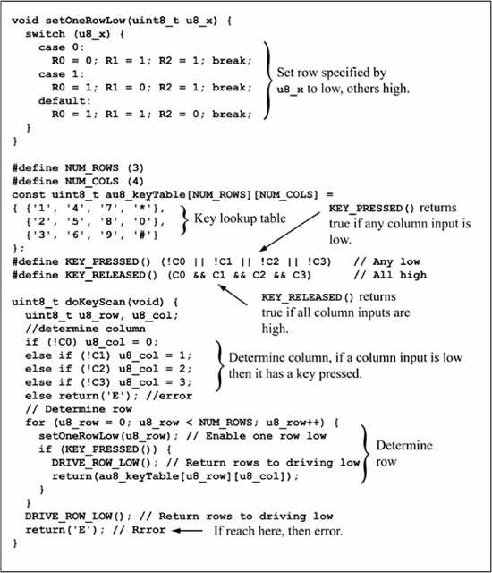
Figure 9.26chap09keypad.c: the ISR and main() code for the keypad interface
On Writing and Debugging ISRs
As discussed previously, when writing ISRs one must be careful not to place too much work within the ISR, as this can either cause other interrupt events to be missed or steal too much time away from the normal program flow. Within an ISR, there should never be a wait for an I/O event—that is the function of the interrupt that triggers the ISR.
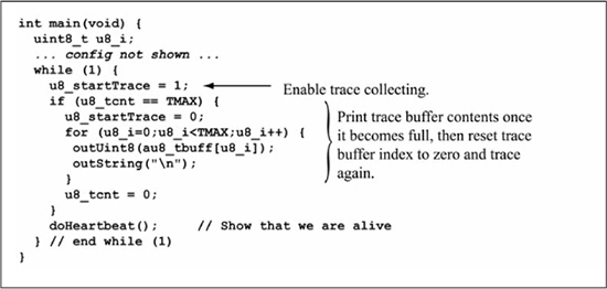
Because many ISRs are time sensitive, putting print statements that output data to a serial port in an ISR to examine ISR variables is often not an option, as this destroys the interrupt timing. It may be valid to place a print statement in the foreground code to examine an ISR variable, but the variable value should always be copied to a temporary variable first because the ISR variable value may be changed by the time the print statement is executed. If you are trying to trace a variable value over several interrupt intervals, then using a print statement may not be an option if the print is not fast enough to monitor the variable value. In this case, a trace buffer can be used in which copies of the variable over several interrupt intervals are kept, then printed when the trace buffer becomes full. Figure 9.27 shows a trace buffer (au8_tbuff) added to the processRotaryData() function of Figure 9.24 to track changes of the rotary encoder state. The current rotary encoder state (u8_curr) is saved if tracing is enabled (u8_startTrace is non-zero) and the trace buffer is not full. The while (1) loop of main() enables tracing, waits for the trace buffer to fill, then prints the contents of the trace buffer. Tracing is re-enabled by emptying the trace buffer (clearing u8_tnct) after the trace buffer is printed.
Figure 9.27chap09
ot_enc_trace.c: using a trace buffer
Summary
The primary use of interrupts is to gain efficiency and responsiveness for LED/switch I/O problems. For mechanical switches such as those used in numeric keypads, this provides an effective debounce mechanism. The next chapter explores the various serial interfaces available on the PIC24 μC and interrupt-driven I/O for those servicing those interfaces, as well as various buffering techniques common to interrupt-driven I/O.
Review Problems
1. Modify the code in Figure 9.5 to generate an address error trap.
2. Modify the code in Figure 9.5 to generate a stack error trap. Why might you want to purposefully trigger a trap error?
3. In Figure 9.9, assume the NOPs in the _CNInterrupt ISR are removed. What happens and why?
4. In Figure 9.9, assume that four NOPs are used in the while (1) loop. What happens and why?
5. Give the CNIExy bit that must be set to enable the change notification on pin RA2 for the dsPIC33EP128GP502.
6. Give the CNIExy bit that must be set to enable the change notification on pin RB7 for the dsPIC33EP128GP502.
7. Write a code sequence that enables the input change notification interrupt for changes on inputs RA4 and RB12 (assume that both have been previously configured as inputs).
8. Write a code sequence that enables the input change notification interrupt for changes on inputs RB10 and RA1 (assume that both have been previously configured as inputs).
9. Assume that for a dsPIC33EP128GP502, the RB13 has a pushbutton switch connected to it, as shown in Figure 9.19, and the change notification interrupt for RB13 is enabled. For the following code snippet, how many times does the _CNInterrrupt ISR execute if the pushbutton is pressed and released one time? Assume no switch bounce and explain your answer.
void _ISR _CNInterrupt(void) {
  DISABLE_RB13_CN_INTERRUPT();     // _CNIEB13 = 0;  (STATEMENT A)
  _CNIF = 0;                       //                (STATEMENT B)
}

int main(void) {
  CONFIG_RB13_AS_DIG_INPUT();
  ENABLE_RB13_CN_INTERRUPT();      // _CNIEB13 = 1;
  _CNIF = 0;                                      (STATEMENT C)
  _CNIP = 2;                                      (STATEMENT D)
  _CNIE = 1;                                      (STATEMENT E)
  while(1);                        // infinite loop
}
10. Repeat problem #9, except remove statement A.
11. Repeat problem #9, except replace statement D with _CNIP = 0.
12. Repeat problem #9, except remove statement E.
13. Figure 9.28 shows one switch connected to INT0 and INT1 interrupt inputs. For the code in Listing 9.7 give the order in which statements A, B, C, and D are executed given a single press and release of SW0. Assume no switch bounce, and explain your answer. Recall that if an INTxEP bit is 1, the interrupt is negative edge triggered; if 0, then it is positive edge triggered.
Figure 9.28
INT0/INT1 interrupt problem
Listing 9.7: Code for INT0/INT1 Interrupt Problem
void _ISR _INT0Interrupt(void) {
  _INT0IE = 0;                                     (STATEMENT A)
  _INT0IF = 0;                                     (STATEMENT B)
}
void _ISR _INT1Interrupt (void) {
  _INT1IE = 0;                                     (STATEMENT C)
  _INT1IF = 0;                                     (STATEMENT D)
}
int main(void) {
  ...config code that enables weak pull-ups...
  _INT0IF = 0;                                     (STATEMENT E)
  _INT0IP = 2;                                     (STATEMENT F)
  _INT0EP = 1;                                     (STATEMENT G)
  _INT0IE = 1;                                     (STATEMENT H)
  _INT1IF = 0;                                     (STATEMENT I)
  _INT1IP = 2;                                     (STATEMENT J)
  _INT1EP = 1;                                     (STATEMENT K)
  _INT1IE = 1;                                     (STATEMENT L)
  while(1);          //infinite loop
}
14. Repeat problem #13, except replace statement J with _INT1IP = 3.
15. Repeat problem #13, except replace statement G with _INT0EP = 0.
16. Repeat problem #13, except replace statement J with _INT1IP = 0.
17. Repeat problem #13, except replace statement L with _INT1IE = 0.
18. Repeat problem #13, except remove statement D.
19. Repeat problem #13, except remove statement D, and replace C with _INT1IE = 1.
20. How many PIC24 Timer2 ticks are equal to 70 μs, assuming a prescale of 1 and a FCY of 20 MHz?
21. How many PIC24 Timer2 ticks are equal to 1.2 ms, assuming a prescale of 8 and a FCY of 30 MHz?
22. What is the maximum PIC24 Timer2 timeout period, assuming a prescale of 64 and a FCY of 30 MHz?
23. What is the maximum PIC24 Timer2 timeout period, assuming a prescale of 8 and a FCY of 10 MHz? Give the answer rounded to the nearest millisecond.
The following problems assume external LEDs (LED1, LED2, and so on) and switches (SW1, SW2, and so on). You may use any of the RBn ports you want to implement these problems. Assume switch inputs are pushbutton inputs and that they use the internal weak pull-up of the port. You may use either Timer2 or Timer3 when a periodic timer interrupt is needed.
24. Assume two LEDs (LED1 and LED2) and one switch input (SW1). Both LEDs should be initially off. After each press AND release of SW1, change the LED state (LED1/LED2) in the sequence: OFF/ON, ON/OFF, ON/ON, OFF/OFF, OFF/ON, ON/OFF, ON/ON, OFF/OFF, and so on. Draw a state machine chart for the problem, with the solution done as in the style of Listing 9.5 (a change notification/timer ISR does all of the work; the while (1) loop is empty).
25. Repeat problem #23, except the LEDs change state whenever a press OR a release occurs for SW1.
26. Assume one LED (LED1) and one switch input (SW1). The LED should be initially blinking. On each press AND release of SW1, alternate between terminating the blinking and resuming the blinking. Draw a state machine chart for the problem, with the solution done as in the style of Listing 9.5 (a change notification / timer ISR does all of the work; the while (1) loop should be empty).
27. Repeat problem #26, except the blinking terminates or resumes whenever a press OR a release occurs for SW1.