
CHAPTER 8
SYSTEM STARTUP AND PARALLEL PORT I/O
This chapter introduces the hardware side of the PIC24 μC family by exploring reset behavior and parallel port I/O for a dsPIC33E μC. In addition, the nuances of writing C code for PIC24 μC applications are examined. As noted, the dsPIC33E offers additional features over the PIC24E with little to no cost difference, motivating its use. However, this book focuses on general-purpose microcontroller usage, rather than digital signal processing; therefore, the term PIC24 will be used to refer to the processor, rather than dsPIC33, to emphasize its general-purpose usage.
Learning Objectives
After reading this chapter, you will be able to:
![]() Implement a simple PIC24 system that has an in-circuit programming interface, a power supply, a serial interface, and a reset switch.
Implement a simple PIC24 system that has an in-circuit programming interface, a power supply, a serial interface, and a reset switch.
![]() Write C code for the PIC24 μC that implements I/O via pushbutton switches and LEDs using a finite state machine approach.
Write C code for the PIC24 μC that implements I/O via pushbutton switches and LEDs using a finite state machine approach.
![]() Discuss the different features of the PIC24 parallel ports such as bidirectional capability, weak pull-ups, and open-drain outputs.
Discuss the different features of the PIC24 parallel ports such as bidirectional capability, weak pull-ups, and open-drain outputs.
![]() Describe the factors that affect dynamic power consumption in CMOS circuits.
Describe the factors that affect dynamic power consumption in CMOS circuits.
![]() Identify common features of integrated circuit datasheets.
Identify common features of integrated circuit datasheets.
![]() Discuss the use of sleep, idle, and doze modes in the PIC24 μC and their effect on power consumption.
Discuss the use of sleep, idle, and doze modes in the PIC24 μC and their effect on power consumption.
![]() Describe the operation of the watchdog timer and its interaction with sleep and idle modes.
Describe the operation of the watchdog timer and its interaction with sleep and idle modes.
![]() Implement a parallel interface between a PIC24 μC and a liquid crystal display module.
Implement a parallel interface between a PIC24 μC and a liquid crystal display module.
High-Level Languages versus Assembly Language
Previous chapters explored the instruction set of the PIC24 μC and assembly language programming in the context of C programming. This was done so that the linkage from high-level language constructs such as data types, conditional statements, loop structures, subroutines, and signed/unsigned arithmetic to assembly language is clear. This understanding is needed, as most programming of microprocessors and microcontrollers is done in a high-level language such as C, not assembly language; therefore, you must be cognizant of the performance and memory usage repercussions when using features of a high-level language. For example, at this point you would not use floating-point data types for convenience (or out of ignorance), but rather would carefully weigh whether the computations required by your application actually need the large number range available with floating-point representation. You now know that using floating-point data types requires more memory space for variables, more program memory for calculations, and in most cases, more execution time for application code. The same tradeoffs apply when weighing the choice between uint32_t/int32_t and uint8_t/int8_t data types, but not on as dramatic a scale as floating-point versus integer types.
Why is most programming of microprocessors and microcontrollers done in a high-level language and not assembly language? One reason is programmer productivity, which is usually measured in the number of debugged code lines produced per day by a programmer. At this point, you know that it generally takes more assembly language statements than C statements to implement the same task, because C statements imply data movement or arithmetic operations that require multiple register transfer operations when mapped to a specific microprocessor architecture. Writing more statements takes more time; hence it generally takes longer to write applications in assembly language than in a high-level language. Another reason is code clarity; code in a higher level language is typically easier to read and understand than assembly language because the fine-grain details of operator implementation are hidden. Another reason is portability; code written in a high-level language is easier to port to another microprocessor than assembly language because it is the compiler’s task to translate the C to the target microprocessor instruction set. This is important, as code is often reused from application to application, and you do not want to lose the time and money invested in creating an application suite if the target microprocessor changes.
So, when is assembly language needed? One reason to write in assembly language is to implement special arithmetic functions that are not available in the high-level language of choice, such as implementing saturating integer arithmetic in C. Another reason is to write a performance-critical section of code in assembly language if the compiler cannot be trusted to produce code that meets required performance specifications. Yet another reason might be to use certain features of the processor that can only be accessed by special instructions within the instruction set. All of these reasons require an understanding of assembly language programming. Even when writing in a high-level language, you should be aware of the features of the instruction set and architecture of the target processor. For example, if the target processor is a 32-bit processor, using 32-bit data types versus 8-bit data types will probably not have much impact on the execution speed of integer operations.
The term embedded system is often applied to microcontroller applications because the microcontroller is hidden within the target system, with no visible external interface. A car typically has tens of microcontrollers within it, yet this fact is not apparent to the car owner. What high-level languages are used to program embedded systems? The C++ language is a popular choice for complex applications written for high-performance microprocessors. However, the C programming language is often the language of choice for an embedded system, as C was intentionally designed to provide tight coupling between C statements and assembly language. In addition, most embedded system programs are control-intensive and do not require complex data structures. Thus, the powerful data abstraction capabilities of an object-oriented programming language such as C++ are often not required in embedded system applications. If a compiler is available for a microcontroller, more often than not it will be a C compiler and not a C++ compiler. This does not mean that there are no microcontroller applications programmed in C++, but rather, that C is the more popular choice, especially for lower-performance microcontrollers. Languages such as Java that are compiled to an intermediate form that is then interpreted by a run-time execution engine are not widely used in microcontroller applications because of the performance loss when compared to an application compiled to the microcontroller’s native assembly language.
This chapter begins the hardware topic coverage in this book. Over the next seven chapters, the details of the major hardware subsystems of the PIC24 μC are explored and sample applications are discussed. The hardware chapters of this book focus on the PIC24E/dsPIC33E branch of the PIC24 μC family, which provide more performance and functionality than the PIC24H/F/FK or dsPIC33F processors. However, the PIC24 and dsPIC33 variants share the same assembly language instruction set [8] and many of the same hardware modules, so porting C programs between various members of the PIC24/dsPIC33 family is not overly difficult when employing the library that accompanies this book. Most of the C interfacing examples in this book are compatible with both families, and the C library functions that are included with this book use conditional compilation to ensure that the code examples operate with both families. To exercise the features of the PIC24 hardware subsystems, application programs that transfer data between the subsystems and memory, configure subsystems for different operating modes, and check subsystem operation status are presented. These programs are written in C to promote code clarity. It is a difficult enough task to grasp the operational details of a hardware subsystem without the additional problem of struggling with long assembly language programs, where the details of memory transfers and arithmetic operator implementation mask the overall program functionality. The previous coverage of the PIC24 μC instruction set and assembly language programming techniques in the context of the C language has prepared you for moving beyond assembly language when discussing the hardware subsystems of the PIC24 μC. In covering the PIC24 μC hardware subsystems, it is expected that you will refer to the PIC24E/dsPIC33E Family Reference Manual (FRM) datasheets [9-30] or the dsPIC33EP128GP502 datasheet [31] when additional details or clarification are needed. This book does not attempt to duplicate all of the information in the PIC24 datasheets, which is clearly impractical and unnecessary. Instead, this book presents key functionality of each subsystem in the context of application examples. In some cases, detailed descriptions of the registers associated with a subsystem and individual register bits are presented in this book; at other times, you are referred to the appropriate datasheet. The ability to read datasheets and extract key information is a necessary survival skill for any person interfacing microprocessors or microcontrollers to other devices. A section in this chapter is devoted to providing tips on datasheet reading for those readers who are encountering datasheets for the first time.
C Compilation for the PIC24 μC
In this book, the C programs for hardware application examples use the MPLAB® XC 16 compiler for the PIC24 from Microchip Technology Inc. From this point onward, this book refers to this compiler as the “PIC24 compiler. In Chapter 2, a compiler is defined as a program that translates statements in a high-level language to assembly language. Figure 8.1 shows a conceptual view of the steps performed in transforming a C program into machine code that can be programmed into the PIC24 μC. The compiler first transforms the C code into unoptimized assembly language, which is done by looking at each C statement individually and implementing it as a sequence of instructions. The optimization stage then looks at groups of assembly language instructions and attempts to reduce the number of instructions by considering data transfer requirements of the entire group. The right side of Figure 8.1 shows an example compiler optimization, in which two C statements are translated into four assembly language instructions when each C statement is considered individually. The optimizer then considers the four assembly language instructions as a group and notes that the W0 register already contains the value of j from the previous operation, so the second mov j,W0 instruction can be removed. This is only a small example, as there are many different types of compiler optimizations that are performed. Typically, code size is reduced and performance improved after optimization.
After optimization, an assembler internal to the compiler translates the assembly language to machine code that is then placed within an object code (.o) file. If a program becomes large, it is good programming practice to split the source code among several files, where each file contains functions that are related to each other. This makes the source code easier to maintain and allows a group of programmers to work on the same microcontroller application concurrently. Thus, an application may have several object files; the linker combines these files into a single file that is executed by the microprocessor. In the case of the PIC24 μC, this “executable” file is a .hex file, which contains an ASCII-hex representation of the program memory contents and is downloaded into the program memory of the PIC24 μC.
Figure 8.1
The compilation process
Special Function Registers and Bit References
A C compiler for a microcontroller must provide access to the special function registers and to individual bits of those registers. In the MPLAB® PIC24 compiler, all special function registers have matching C declarations contained in a header file (.h) that is particular to the target device. For example, a special function register used for parallel port I/O and discussed later in this chapter is named PORTB, whose memory location is 0xE12. In the PIC24 compiler installation directory, a file named C:Program Files (x86)Microchipxc16v1.20supportdsPIC33Ehp33EP128GP502.h is the header file used for the dsPIC33EP128GP502 μC. Within this file is contained the following line that defines the special function register PORTB as an unsigned int (16-bit) data type.
extern volatile unsigned int PORTB __attribute__((__sfr__));
The __attribute__ keyword is an extension to standard C by the PIC24 compiler that allows variable and function attributes to be defined, allowing for specific actions to be taken by the compiler based on the attribute values. The __attribute__((__sfr__)) annotation specifies that PORTB is a special function register. A separate linker file assigns the location 0xE12 to the PORTB variable. The PORTB variable declaration allows the entire PORTB special function register to be written or read with a single C statement:
PORTB = 0x3010; // Assign PORTB a value.
An individual bit of PORTB can be tested using a bitwise & operation, as was initially done in Chapter 4. The following code fragment executes the if-body if the least significant bit of PORTB is a 1:
if (PORTB & 0x0001) {
  // Execute if-body if LSb of PORTB is 1.
}
Because operations on individual bits within special function registers are commonplace, almost all SFRs also have C struct data type definitions that allow convenient access to individual bits and bit fields. For example, within the same header file is a C struct definition named PORTBBITS that defines individual bit names for each of the 16 bits of PORTB:
typedef struct tagPORTBBITS {
  unsigned RB0:1;
  unsigned RB1:1;
  unsigned RB2:1;
  unsigned RB3:1;
  unsigned RB4:1;
  unsigned RB5:1;
  unsigned RB6:1;
  unsigned RB7:1;
  unsigned RB8:1;
  unsigned RB9:1;
  unsigned RB10:1;
  unsigned RB11:1;
  unsigned RB12:1;
  unsigned RB13:1;
  unsigned RB14:1;
  unsigned RB15:1;
} PORTBBITS;
The :1 after each struct element name indicates the bit width of the named element. The following line defines a variable named PORTBbits of type PORTBBITS:
extern volatile PORTBBITS PORTBbits __attribute__((__sfr__));
The PORTBbits variable definition allows individual bits of PORTB to be referred to as PORTBbits.RBn, where n is the bit number. The following code snippet sets bit 5 of PORTB and clears bit 2 of PORTB.
PORTBbits.RB5 = 1;   // Set bit 5 of PORTB.
PORTBbits.RB2 = 0;   // Clear bit 2 of PORTB.
These C statements are mapped by the compiler into assembly language bset and bclr instructions for an efficient implementation. Individual bits can be tested using similar references; the following code fragment executes the if-body if the least significant bit of PORTB is a 1:
if (PORTBbits.RB0) {
  // Execute if-body if LSb of PORTB is 1.
}
Likewise, the common use of multi-bit fields in SFRs is supported in C. For example, the OSCCON register contains several fields:
typedef struct tagOSCCONBITS {
  union {
    struct {
      unsigned OSWEN:1;
      unsigned :2;
      unsigned CF:1;
      unsigned :1;
      unsigned LOCK:1;
      unsigned IOLOCK:1;
      unsigned CLKLOCK:1;
      unsigned NOSC:3;
      unsigned :1;
      unsigned COSC:3;
    };
    struct {
      unsigned :8;
      unsigned NOSC0:1;
      unsigned NOSC1:1;
      unsigned NOSC2:1;
      unsigned :1;
      unsigned COSC0:1;
      unsigned COSC1:1;
      unsigned COSC2:1;
    };
  };
} OSCCONBITS;
extern volatile OSCCONBITS OSCCONbits __attribute__((__sfr__));
This definition allows access to the entire NOSC bit field composed of three bits using statements such as OSCCONbits.NOSC = 2; or to individual bits by equivalently executing OSCCONbits.NOSC2 = 0; OSCCONbits.NOSC1 = 1; OSCCONbits.NOSC0 = 0;.
Finally, the same header file has C macros that provide a shorthand reference for many of the SFR named bits and bit fields that eliminate the need to remember the SFR register name. A C macro in its simplest form allows one or more C statements to be referred to by a single label, which is the macro name. A macro is defined using the #define statement. For the PORTB bits, these macros are:
#define _RB0 PORTBbits.RB0
#define _RB1 PORTBbits.RB1
#define _RB2 PORTBbits.RB2
#define _RB3 PORTBbits.RB3
#define _RB4 PORTBbits.RB4
... etc., other RBn  macros not shown....
This allows the previous code snippet that set bit 5 and cleared bit 2 of PORTB to be written as:
_RB5 = 1;   // Set bit 5 of PORTB.
_RB2 = 0;   // Clear bit 2 of PORTB.
Similarly, a bit test of the LSb of PORTB can be written as:
if (_RB0) {
  // Execute if-body if LSb of PORTB is 1.
}
Likewise, macros are provided in the header file that access the bit fields:
#define _OSWEN OSCCONbits.OSWEN
#define _CF OSCCONbits.CF
#define _LOCK OSCCONbits.LOCK
#define _IOLOCK OSCCONbits.IOLOCK
#define _CLKLOCK OSCCONbits.CLKLOCK
#define _NOSC OSCCONbits.NOSC
#define _COSC OSCCONbits.COSC
#define _NOSC0 OSCCONbits.NOSC0
#define _NOSC1 OSCCONbits.NOSC1
#define _NOSC2 OSCCONbits.NOSC2
#define _COSC0 OSCCONbits.COSC0
#define _COSC1 OSCCONbits.COSC1
#define _COSC2 OSCCONbits.COSC2
Therefore, the value of the bit field NOSC can be in one statement as _NOSC = 2; or by setting each bit of the field by using _NOSC2 = 0; _NOSC1 = 1; and_NOSC0 = 0;.
The macro definitions for named bits and bit fields are only defined for unique bit names; they are not defined if the same bit name is used in more than one special function register. This book uses the macro definition for named bits wherever possible because this means that only the bit name has to be remembered, and not the special function register name.
PIC24 Compiler Run-Time Code, Variable Qualifiers/Attributes
Run-time code is code generated by the compiler and executed by the processor before the main() function is entered. The run-time code produced by the PIC24 compiler performs the following steps:
![]() Initializes the stack pointer and stack limit registers. The default actions maximize the amount of available stack space.
Initializes the stack pointer and stack limit registers. The default actions maximize the amount of available stack space.
![]() Initializes all global variables; if an initial value is not specified for a global variable, then it is cleared.
Initializes all global variables; if an initial value is not specified for a global variable, then it is cleared.
![]() Initializes the PSV register so that constant data placed in program memory can be accessed.
Initializes the PSV register so that constant data placed in program memory can be accessed.
![]() Calls
Calls main(); if the main() function returns then the processor is reset by executing the reset instruction. It should be noted that returning from the main() function is rarely done in embedded applications; the examples later in this chapter never return from main().
Some attributes and variable qualifiers used in the example C programs in the hardware chapters are the const qualifier and the persistent attribute. The const qualifier for a variable indicates that the program does not change the variable from its initial contents. The default action of the compiler is to place all const variables in program memory to reduce RAM usage. The const qualifier is typically used with constant strings and arrays, such as shown here:
const uint8_t sz_hellomsg[] = “Hello World!”;
const uint8_t au8_table[] = {0x23, 0xA0, 0x7F, 0x39};
The persistent attribute, when applied to a variable, causes the variable to be uninitialized by the run-time code. This allows the variable to track values between processor resets; one usage of persistent variables is for communicating error status after a reset. The persistent attribute applied to a variable is shown here:
uint8_t u8_resetCount __attribute__((persistent));
You will use a macro form of this named _PERSISTENT, defined by the processor-specific header file (such as p33EP128GP502.h), as follows:
uint8_t _PERSISTENT u8_resetCount;
C Macros, Inline Functions
The example C programs in the hardware chapters make extensive use of C macros as a method of improving code clarity.
An all-uppercase naming convention is used for macros in these programs. These are defined in various header files, either written by the authors or provided with the PIC24 compiler. So, when you see a C statement such as:
CONFIG_RB11_AS_DIG_OUTPUT();
be aware that CONFIG_RB11_AS_DIG_OUTPUT() is a C macro function whose definition is found in one of the included header files. The first time that a particular macro type is used in an example program, I explain the macro’s functionality and show the C statements that the C macro represents.
Conditional Compilation
Conditional compilation allows C statements to be either processed or ignored based on a macro definition or macro value. For example, different include files are used depending on processor type:
#if defined(__dsPIC33EP128GP502__)
#include <p33EP128GP502.h>
#endif

#if defined(__dsPIC33EP128GP504__)
#include <p33EP128GP504.h>
#endif

#if defined(__dsPIC33EP128GP506__)
#include <p33EP128GP506.h>
#endif
... other code omitted ...
The chained if/elif conditional statements (if/else if) include file p33EP128GP502.h if macro __dsPIC33EP128GP502__ is defined, while file p33EP128GP504.h is included if macro __dsPIC33EP128GP504__ is defined, and so on. The macros __dsPIC33EP128GP502__, __dsPIC33EP128GP504__, and so on, are defined by the compiler based on the μC device setting in MPLAB®, which allows device-specific C code to be generated. The #ifdef statement can be used instead of defined(), so the following:
#ifdef __dsPIC33EP128GP502__
#include <p33EP128GP502.h>
#endif
#if defined(__dsPIC33EP128GP502__)
#include <p33EP128GP502.h>
#endif
The #ifndef macroname and #if !defined(macroname) tests can be used to detect if a macro is not defined. The macros __dsPIC33E__, __PIC24E__, and so on, are also defined by the compiler for conditional compilation based on processor family such as:
#if defined(__dsPIC33E__) || defined(__PIC24E__)
    case 6:  outString(“Fast RC Osc/16
”); break;
    case 7:  outString(“Fast RC Osc/N
”); break;
#elif defined(__PIC24F__)
    case 7 : outString(“Fast RC Osc with Postscale”); break;
#else
#error Unknown processor
#endif
A macro’s value can also be used for controlling conditional compilation, as shown in the following code snippet:
#if (NUM_UARTS >= 2)
    case 2 :
      __C30_UART = 2;   // This is the default UART.
      configUART2(u32_baudRate);
      break;
#endif
The #if (NUM_UARTS >= 2) test includes the code that follows only if the value of NUM_UARTS is greater than or equal to 2. Macros are defined and assigned values within a source file as follows:
#define NUM_UARTS (2)         // NUM_UARTS = 2
#define UART1_TX_INTERRUPT   // UART1_TX_INTERRUPT macro defined, no value.
When defining a macro, be sure to surround its definition with parentheses, to avoid a number of subtle problem: use #define NUM_UARTS (2), not #define NUM_UARTS 2. Macros can also be passed to the compiler by the -D flag, as in -DNUM_UARTS=(2) and -DUART1_TX_INTERRUPT. Macros can also be defined and assigned values within an MPLAB® project file, which are then passed to the compiler using the -D flag.
More information on the MPLAB® PIC24 compiler operation can be found in the MPLAB® XC16 C Compiler User’s Guide [32], found in the docs/ subdirectory of the PIC24 compiler installation directory.
PIC24 Startup Schematic
The version of the PIC24 μC used in most of the interfacing examples in this book is the dsPIC33EP128GP502 μC, whose pin diagram is given in Figure 8.2. This device has 128 Ki bytes of program memory, 32 Ki bytes of SRAM, and is suitable for experimentation on a protoboard given its small footprint of 28 pins provided in a dual in-line package (DIP). An external pin usually has more than one internal function mapped to it because of the limited number of pins on the 28-pin package. Control bits within special function registers determine the mapping of internal functions to external pins.
For additional hardware platforms and options, see the getting started guide on the companion website (www.reesemicro.com).
Figure 8.2
dsPIC33EP128GP502 pin diagram
Source: Figure redrawn by author from dsPIC33EP128GP502 datasheet (DS70000657H), Microchip Technology Inc.
A brief summary of many of the pin functions used in this book is given here; more details are provided in the appropriate chapter covering that functionality.
![]() VDD,VSS: These are power (VDD) and ground (VSS) pins; observe that there is more than one ground pin. Integrated circuits typically have multiple power and ground pins, all of which must be connected.
VDD,VSS: These are power (VDD) and ground (VSS) pins; observe that there is more than one ground pin. Integrated circuits typically have multiple power and ground pins, all of which must be connected.
![]() AVDD, AVSS: These are power (AVDD) and ground (AVSS) pins for the analog modules, which are discussed in Chapter 11. Even if the analog modules are not used, these must be connected to power and ground for the PIC24 to operate correctly.
AVDD, AVSS: These are power (AVDD) and ground (AVSS) pins for the analog modules, which are discussed in Chapter 11. Even if the analog modules are not used, these must be connected to power and ground for the PIC24 to operate correctly.
![]() VCAP/VDDCORE: The internal voltage used by the microcontroller is available on this pin.
VCAP/VDDCORE: The internal voltage used by the microcontroller is available on this pin.
![]() MCLR#: This input pin resets the device when brought low. The # symbol in the name indicates a low-true signal.
MCLR#: This input pin resets the device when brought low. The # symbol in the name indicates a low-true signal.
![]() PGEC1/PGED1, PGEC2/PGED2, PGEC3/PGED3: Any of the PGECx/PEGDx pin pairs can be used for In-Circuit Serial Programming (ICSP), which is the process of downloading a program into the device using an external programmer without removing the device from the board.
PGEC1/PGED1, PGEC2/PGED2, PGEC3/PGED3: Any of the PGECx/PEGDx pin pairs can be used for In-Circuit Serial Programming (ICSP), which is the process of downloading a program into the device using an external programmer without removing the device from the board.
![]() OSCI, OSCO: These pins can be used with an external crystal to provide the main clock source for the device (details in this chapter).
OSCI, OSCO: These pins can be used with an external crystal to provide the main clock source for the device (details in this chapter).
![]() CLKI, CLKO: An external clock can be provided via the CLKI input pin, while the internal clock can be monitored via the CLKO output pin.
CLKI, CLKO: An external clock can be provided via the CLKI input pin, while the internal clock can be monitored via the CLKO output pin.
![]() RAn, RBn: These pins are parallel port I/O pins (details in this chapter).
RAn, RBn: These pins are parallel port I/O pins (details in this chapter).
![]() ANn, VREF–, VREF+: The ANn inputs are the analog inputs for the analog-to-digital converter subsystem (Chapter 11). The VREF–/VREF+ pins are used to provide negative and positive voltage references for the analog-to-digital converter.
ANn, VREF–, VREF+: The ANn inputs are the analog inputs for the analog-to-digital converter subsystem (Chapter 11). The VREF–/VREF+ pins are used to provide negative and positive voltage references for the analog-to-digital converter.
![]() ASCL1/ASDA1, SCL1/SDA1: These pin pairs implement the I2C synchronous serial data interface (details in Chapter 10).
ASCL1/ASDA1, SCL1/SDA1: These pin pairs implement the I2C synchronous serial data interface (details in Chapter 10).
![]() RPn/RPIn: These are remappable peripheral pins that allow internal pin functions to be connected in a flexible manner to external I/O pin (details in Chapters 9 and 10).
RPn/RPIn: These are remappable peripheral pins that allow internal pin functions to be connected in a flexible manner to external I/O pin (details in Chapters 9 and 10).
![]() INT0: This is an external interrupt pin (details in Chapter 9).
INT0: This is an external interrupt pin (details in Chapter 9).
![]() T1CK: This input can be used to provide a clock for Timer1 (details in Chapter 12).
T1CK: This input can be used to provide a clock for Timer1 (details in Chapter 12).
A schematic used to test PIC24 functionality by flashing a light emitting diode (LED) is shown in Figure 8.3. The schematic functionality can be split into power, reset, serial communication, in-circuit serial programming, and application components. If you are somewhat rusty at recognizing electrical symbols, review the material in Appendix B that provides a hobbyist-level review of basic circuit theory. You only need a hobbyist-level intuition about basic circuit concepts for the interfacing topics in this book; a detailed circuit analysis background is not required.
Figure 8.3
PIC24 startup schematic for flashing an LED
Startup Schematic: Power
The PIC24 requires that the input voltage VDD be in the range 3.0 V to 3.6 V. An external AC-to-DC wall transformer (or 9 V battery) provides power that outputs 9 V unregulated, which means that the output voltage can fluctuate depending on the amount of current that is drawn. An LM2937-3.3 voltage regulator is used to provide a stable 3.3 V output as the VDD for this system (see www.reesemicro.com for a complete list of the components used in the interfacing examples of this book as well as a picture of a completed protoboard layout). The LM2937 accepts a wide input voltage (4.75 V to 26 V); 9 V is used for example purposes. The 3.3 V voltage on the PIC24 VDD pin is connected to a voltage regulator internal to the PIC24 μC that provides a digital core voltage of 1.8 V. The fuse in the power path is a safety precaution; it will blow (no longer conduct current) if excessive current is drawn from the power supply. Excessive current can be drawn if a short (a low-resistance path) is created between VDD and VSS by a wiring mistake during circuit hookup or by component failure.
The total current required for this PIC24 μC system after all peripheral chips have been added is under 100 mA (1 mA = milliAmperes = 0.001 A). A 500 mA wall transformer provides a margin for hardware experiments that use higher current draw devices, such as a DC motor for driving the wheel of a small robot. The C1 capacitor is required by the LM2937 for output voltage stability with a minimum suggested value of 10 μF and maximum ESR (equivalent series resistance) of 5 Ω. The 0.1 μF C2, C4, and C5 and 10 μF C3 capacitors are called decoupling capacitors and assist in supplying transient current needs caused by high-frequency digital switching. These capacitors should be placed as close as possible to their respective power and ground pins (VDD, VCAP, AVDD, VSS, and AVSS) for maximum effectiveness. All four capacitors need to have low ESR, such as provided by low ESR tantalum and ceramic capacitors, with ceramic capacitors having lower ESR than tantalums at equivalent capacitor values. The C3 capacitor is especially critical as it helps maintain the stability of the PIC’s internal voltage regulator; the PIC24 datasheet recommends an ESR of less than 1 Ω. The L1 LED is used in two roles—the first is as a power status since the LED is on when power is applied. The second role is as an LED that can be blinked by the PIC24 via the connection from port RB15 to the LED, as shown in Figure 8.3. Because the power supply and RB15 are both driving the LED, the RB15 port is configured as an open-drain output, which means that it can be driven in two states: (a) low, pulling the LED to ground and turning it off, or (b) high impedance (floating, no drive current supplied), which turns on the LED if power is applied. Open-drain outputs are discussed in more detail later in this chapter; open-drain mode is used in this case to reduce component count and wiring (another LED and series resistor could have been used on R15 instead of sharing the power LED).
To determine the resistance value of R1, note that when RB15 is pulling low (turning off L1), current flows from VDD through the resistor and into RB15. The DC specifications in the dsPIC33EP128GP502 datasheet [31] state that the RB15 pin can sink a maximum of 5 mA over its full temperature range. Solving Ohm’s law (V=IR) for resistance gives R=V/I, with the minimum resistance allowed computed as 3.3 V/5 mA = 660 Ω. The value 910 Ω provides a safety margin and is compatible with the older PIC24H family, which is limited to a maximum of 4 mA of sink current. The current flowing through the LED for RB15 in the high impedance (floating) state is (VDD – LED_Vdrop)/R1, where LED_Vdrop is the voltage drop across the LED. The LED voltage drop can be found on its datasheet for a range of currents, with a typical value of 2 V. Thus, the ON current supplied to the LED by the power supply is (3.3 - 2.0)V/910 Ω = 1.4 mA, which is enough to illuminate a typical LED.
Startup Schematic: Reset
When power is applied to the PIC24, the device performs a power-on reset (POR), which means that the program counter is cleared to 0 and the first instruction is fetched from location 0. This is an internally generated power-on reset sequence; some microcontrollers require an external reset circuit that asserts an input pin either high or low to trigger reset after power is applied. It is also convenient to have a manual reset capability during testing to restart a program without needing to cycle power. The momentary pushbutton connected to the MCLR# input applies a low voltage to MCLR# when pushed, causing the PIC24 μC to reset. The 10 kΩ (R3) resistor that connects the MCLR# pin to VDD is called a pull-up resistor, because it keeps the MCLR# input pulled up to almost 3.3 V when the pushbutton is released. If the pull-up resistor is removed, and a direct connection is made from MCLR# to VDD, a short is created when the pushbutton is pressed, causing excessive current flow and probably causing the fuse to blow. If the pull-up resistor and VDD connection is not made at all, the input varies, or floats between 0 V and VDD when the pushbutton is not pressed. A floating input can read as 0 or 1, depending on the switching activity of nearby pins, causing spurious circuit operation. A PIC24 μC with a floating MCLR# input can experience intermittent resets, a problem that is difficult to debug.
Startup Schematic: PC Serial Communication Link
The example programs use functions that read or send ASCII-encoded strings to a personal computer (PC) using a serial interface known as RS232 (more details about this protocol are covered in Chapter 10). The ASCII-encoded strings exchanged between the PIC24 μC and PC are used for status and debugging messages and for data entry. A serial interface transmits data one bit at a time; Chapter 10 discusses the various serial interfaces implemented by the PIC24 μC. The J2 6-pin header represents a USB-to-RS232-serial cable from FTDI (Future Technology Devices International Limited) that is used to connect the PIC24 μC to the USB (universal serial bus) port of a PC. The FDTI TTL-232R-3.3 USB-to-TTL-serial cable referenced in Figure 8.3 is convenient in that the cable’s TXD (transmit data) and RXD (receive data) pins can be connected directly to the PIC24 μC without any additional circuitry because these pins use 0 to 3.3 V logic levels (other USB-to-serial cables may require an integrated circuit that converts from RS232 logic levels to CMOS levels; see Chapter 10 for more details). The TXD pin on the TTL-232R-3.3 cable transmits serial data from the PC to the PIC24 μC, while the RXD pin implements communication in the reverse direction from the PIC24 μC to the PC. The example programs use the RB10/RB11 pins on the PIC24 μC for the RX/TX functions required by the serial interface. The GND pin (1) on the FDTI TTL-232R-3.3 cable must be connected to the GND of the PIC24 μC. The 5 V power pin (3) of the FDTI TTL-232R-3.3 cable can be used as an alternative power supply for the LM2937-3.3 voltage regulator, but you must be careful not to exceed the maximum current limit of 500 mA allowed to a USB device.
Startup Schematic: In-Circuit Serial Programming
The J1 6-pin header and their connections are optional; these are used for in-circuit serial programming of the PIC24 μC using an external programmer such as the inexpensive PICkit3 programmer available from Microchip (see the ICSP programmers section at http://www.reesemicro.com/Home/pic24-software-library-collection/getting-started). The PICkit3 external programmer applies a clock (PGEC1), a serial data stream (PGED1), and an MCLR# signal when downloading a hex file into program memory. The advantage of in-circuit serial programming is that the PIC24 μC does not have to be removed from the board during programming. Any of the PGECn/PGEDn input pairs can be used for the ICSP operation.
Startup Schematic: Application Components
The power, reset, serial communication, and in-circuit programming components of the startup schematic will remain unchanged through most of the interfacing examples in the remaining chapters. Each interfacing example will typically add components for the particular application. The first application program flashes the L1 LED, which is a common method for proclaiming that “I am alive!” when testing a microcontroller system for the first time. See the getting started guide of the companion website (www.reesemicro.com/Home/pic24-software-library-collection/getting-started) for instruction on transferring a program, such as ledflash.c, to your PIC24 μC.
ledflash.c—The First C Program for PIC24 Startup
The C code of Figure 8.4 flashes the L1 LED connected to pin RB15 in Figure 8.3. The source code for this program is contained in chap08ledflash_nomacros.c, freely downloadable from the PIC24 library at www.reesemicro.com, as indicated by the title in Figure 8.4. All following figures likewise give the path to the source code under discussion. The statement #include “pic24_all.h” includes a standard header file used in this book’s examples; the header file’s contents are discussed later in this chapter.
Figure 8.4 is the first C code listing for PIC24 μC hardware experiments presented in this book. Because of space considerations, the C source code given in the figures is typically not complete—the figure source code will usually omit C functions previously covered or omit include statements for various header files. All of the C source code files used in book figures that illustrate PIC24 μC hardware features are included on the companion website (www.reesemicro.com) in their complete form; use these source files when attempting to duplicate the experiments.
Clock Configuration
The first statement of main() is a call to the function configClock() that configures the PIC24 clock source. The configClock() function is located in the file libsrcpic24_clockfreq.c in the source file distribution for this book. The PIC24 family has several methods for clock generation, which are mentioned later in this chapter; the default method used by the examples in this book is the internal oscillator option configured for the maximum clock frequency of 120 MHz (FOSC). From Chapter 3, recall that if FOSC = 120 MHZ, then the instruction cycle time FCY is FCY = FOSC/2 = 60 MHz. Using the internal oscillator has the advantage of less wiring for the startup schematic since a clock source does not have to be provided; the clock is generated internally by the PIC24 μC.
Figure 8.4chap08ledflash_nomacros.c: C code for flashing an LED
Flashing the LED
Pin RB15 is a bidirectional, parallel port pin, also referred to as a parallel input/output (PIO) pin. The term bidirectional means that the pin can be configured either as an input or as an output. The RB15 pin must be configured as an output to drive the LED, which is accomplished by the statement _TRISB15 = 0. Each bit of the special function register TRISB controls the direction of the corresponding PORTB bit. A 1 in a TRISB bit configures the corresponding PORTB pin as an input (as a memory hint, 1 looks like I for input), while a 0 configures the PORTB pin as an output (0 looks like O for output). Furthermore, the output drive type is open-drain because you are sharing the L1 LED with the power status as stated earlier, and configuration for open-drain operation is accomplished by the statement _ODCB15 = 1. Additional details on parallel port I/O are given later in this chapter. The statement _LATB15 = 0 assigns a zero to the RB15 data latch, thus driving the RB15 pin low and turning off the LED. The statement while (1) creates an infinite loop, whose loop body first calls a software time delay function named a_delay(), then toggles the value of the RB15 output with the statement _LATB15 = !_LATB15. The software delay function a_delay() is composed of two nested for counting loops. The total delay time is dependent upon the number of instructions executed in the nested for loops and the clock frequency of the PIC24 μC. The delay can be increased or decreased by changing the initial values of the count variables u16_i, u16_k in the nested for loops of the a_delay() function. The delay must be long enough so that the LED can fully turn off or turn on between RB15 pin assignments. If the delay is too short, the LED will appear always on (though dim), even though an oscilloscope trace would reveal that RB15 is transitioning between low and high voltages (a square wave output). Software delays are easy to implement, but hardware timers are much better at creating accurate time delays. The timer subsystem of the PIC24 μC and its usage is first discussed in Chapter 9, and covered in more detail in Chapter 12. Observe that the only method of terminating the while (1) loop in Figure 8.4 is by cycling power or reset via the pushbutton on MCLR#. This infinite loop nature is typical of microcontroller applications because if the loop is exited, there is nowhere to go!
An Improved LED Flash Program
Figure 8.5 shows an alternative version of the LED flash code that uses C macros for improving code clarity and for encapsulating I/O pin assignments.
Figure 8.5chap08ledflash.c: Improved code example for flashing an LED
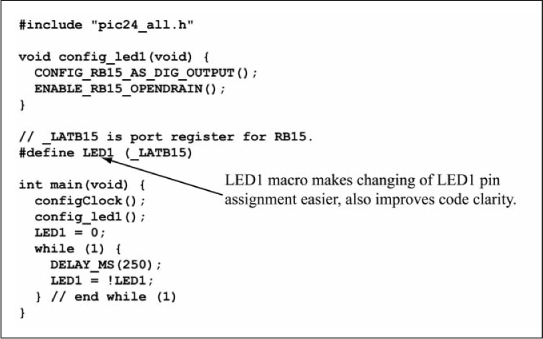
The config_led1() function replaces the original statements _TRISB15 = 0, _ODCB15 = 1 that configured RB15 as an open-drain output. The reason for this change is to improve code clarity; an external reader can guess from the function name that this configures an I/O pin used for driving an LED in the program. The config_led1() function definition simply uses two other macros named CONFIG_RB15_AS_DIG_OUTPUT() and ENABLE_RB15_OPENDRAIN() that contain the statements _TRISB15 = 0, _ODCB15 = 1. Again, the purpose of these macros is for improved readability; remembering that _TRISB15 = 0 configures the RB15 pin as an output and not as an input can be difficult. However, the macro name CONFIG_RB15_AS_DIG_OUTPUT() is more helpful as to what this macro accomplishes (the DIG is shorthand for digital).
All uses of _LATB15 in the code of Figure 8.4 are now replaced by LED1, which is a macro defined as _LATB15. Note that _LATB15 is wrapped in parentheses, to avoid unwanted side-effects caused by macro substitution—for example, #define A_PLUS_B a+b when used in A_PLUS_B*2 evaluates as a + (b*2), not the expected (a + b)*2. Many other subtle problems exist that parentheses help eliminate. All macros should be wrapped in parentheses to avoid these problems. This improves code clarity as now it is clear when the LED is affected by the code, instead of having to remember that RB15 drives the LED. Furthermore, if you want to move the LED to a different pin, you only have to change the LED1 and CONFIG_LED1 macros. This is the greatest benefit of using macros to isolate pin assignments as it is a common desire to want to reuse sample interfacing code with different pin assignments.
Finally, the a_delay() software delay function call is replaced by DELAY_MS(250) where the macro DELAY_MS(ms) implements a delay of approximately ms milliseconds. The DELAY_MS macro is defined in the libincludepic24_delay.h file in the book source distribution, and is shown here.
#define DELAY_MS(ms)
  delayAndUpdateHeartbeatCount(CYCLES_PER_MS * ((uint32_t) (ms)));
The delayAndUpdateHeartbeatCount(uint32_t u32_cyc) function called by DELAY_MS is also defined in libincludepic24_delay.h as:
inline static void delayAndUpdateHeartbeatCount(uint32_t u32_cyc) {
  __delay32(u32_cyc);
  u32_heartbeatCount += (u32_cyc >> 4);
}
It delays u32_cyc instruction cycles by calling the __delay32(uint32_t u32_cyc) function provided by the PIC24 compiler support library. The u32_cyc variable passed to delayAndUpdateHeartbeatCount is the number of instruction cycles that execute in ms milliseconds. The CYCLES_PER_MS macro is the number of instructions cycles that execute in one millisecond, and is defined in libinclude pic24_clockfreq.h as:
#define CYCLES_PER_MS ((uint32)(FCY * 0.001))
The FCY macro is set to the instruction cycle frequency. When using the default clock configuration discussed later in this chapter (see “Clock Generation”), its value is defined in libincludepic24_ clockfreq.h to be 59881250L (~60 MHz). Note the trailing L makes the number a long (equivalent to a uint32_t), causing the compiler to allocate a 32-bit value in which to store the number.
For example, with FCY = 60 MHz, 1 ms = 60,000 instruction cycles. The u32_heartbeatCount variable updated in the delayAndUpdateHeartbeatCount() function is discussed in the next section. The libinclude pic24_delay.h file also includes a DELAY_US(us) macro that delays us number of microseconds. The DELAY_MS() and DELAY_US() macros should only be used for approximate timing; the hardware timers covered in Chapter 12 provide more accurate timing.
echo.c—Testing the Serial Link
The subsystem of the PIC24 μC that performs serial communication over the RX/TX pins shown in the startup schematic of Figure 8.3 is called the UART (universal asynchronous receiver transmitter). The UART subsystem is covered in detail in Chapter 10; this section discusses from a user-level perspective some of the functions for receiving/transmitting ASCII data over the serial link. The internals of these functions are discussed in Chapter 10. The C code of Figure 8.6 tests the serial link by printing some status messages, then enters an infinite while (1) loop that waits for a single character to be received from the serial link using the inChar() function. The received character is placed in the u8_c variable, incremented, then written back to the serial link using the outChar() function. This means a received character of S is echoed as T, a 1 as 2, a d as e, and so on. The received character is incremented to verify that the PIC24 μC is actually reading and transmitting the character; if the character were transmitted back without modification then a short circuit between the RX and TX lines could mimic this behavior. Both the inChar() and outChar() functions are defined in libsrcpic24_serial.c.
Figure 8.6chap08echo.c: Program for testing the serial link
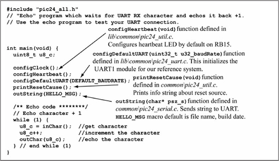
The code of Figure 8.6 has some new functions that are executed before the while (1) loop is reached. These functions are:
![]()
configHeartbeat(): When debugging a μC system, a basic question that often arises is “How do I know if the μC is alive and executing code?” The example programs reserve the RB15 pin for a heartbeat that is used to blink an attached LED. In any of the functions that perform a potentially long wait, such as inChar() that waits for arrival of a character over the serial link, the code will pulse the LED attached to the RB15 pin to indicate that the μC is alive. The heartbeat update is performed by an associated function called doHeartbeart() that is called from a user function to increment a uint32_t global variable named u32_heartbeatCount. Once the u32_heartbeatCount variable reaches a maximum value set within configHeartBeat(), the heartbeat LED is toggled and the u32_heartbeatCount is reset to 0. The heartbeat functions are found in libsrcpic24_util.c. It should be noted that the heartbeat LED functions as a debugging tool and would not be typically included in a production design.
![]()
configDefaultUART(uint32_t u32_baudRate): This function configures the UART subsystem to transmit serial data at the rate specified by the u32_baudRate parameter. There is a range of standard data rates for this type of serial link; these are defined in Chapter 10. The data rate defined by the DEFAULT_BAUDRATE macro is 230,400, which means that bits are sent at roughly 230,400 bits per second. This function is defined in libsrcpic24_serial.c.
![]()
printResetCause(): The function prints an information string about the cause of the last processor reset. A section later in this chapter discusses the various sources of CPU reset. The function also identifies the target processor, its revision number, and the clock option currently being used. This function is defined in libsrcpic24_util.c.
![]()
outString(const char* psz_s): This function transmits each character of null-terminated string over the serial link. The function assumes an ASCII-encoded string is being transmitted. The HELLO_MSG is a macro defined in libincludepic24_uart.h with a default value of the file name and build date of the program being compiled (in this case, echo.c).
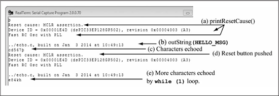
To test the serial link, the bootloader included in the library distribution accompanying this book (see www.reesemicro.com) is run on the PC to display the received characters from the PIC24 μC and to transmit keyboard input back. Other options include RealTerm, PuTTY, and Tera Term. Follow instructions in the getting started guide at www.reesemicro.com to program and communicate with your PIC24.
Figure 8.7 shows the echo.c program output in the RealTerm console window. The printResetCause() function identifies the reset cause as “Power-on” when power is applied, and then as “MCLR assertion” when the Reset button is pushed at (d). The displayed characters echoed in (c) and (e) are 1+ the ASCII values of the characters typed from the keyboard.
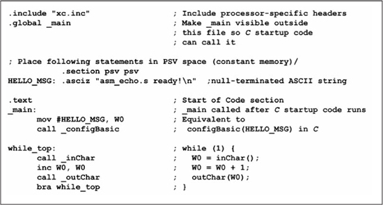
asm_echo.s—Implementing Echo in Assembly
The assembly language skills you learned in the previous chapters can also be used to write assembly-language programs that make use of the C functions previously discussed, as shown in Figure 8.8. This assembly code implements the echo.c code of Figure 8.6. This code calls a new C function named configBasic(const char* sz_helloMsg), defined in libsrcpic24_util.c. This function combines the individual configuration calls used in echo.c, such as configClock(), configHeartbeat(), and so on, into one convenient function. The sz_helloMsg parameter is a message printed to the console after configuration is complete. Note that all C functions have an appended underscore when referenced from assembly, so the C function configBasic becomes _configBasic in the assembly code, inChar becomes _inChar, and outChar becomes _outChar.
As in earlier assembly-language programs, the first line begins by including processor-specific headers given in xc.inc. To define a string, the .section psv psv directive instructs the assembler to place following statements in the Program Space Visibility region where C stores and accesses constants. The .asciz directive then places the “asm_echo.s ready!
” string in the PSV area. After switching to the code section with a .text directive, the .global _main statement makes the _main label visible outside this file, so that the C start-up routines can call it after initializing C variables. Next, the mov #HELLO_MSG, W0 statement places the address of the hello message in W0, the first parameter expected by the configBasic function. The statement call _configBasic calls this function, which performs basic chip configuration as previously discussed. Next, the inChar() C function is called, which reads a character from the serial port and returns it in W0. The returned character is then incremented and sent back over the serial port by a call to outChar. Finally, a bra while_top statement loops back to the inChar() function call to repeat the process.
Figure 8.8chap08asm_echo.s: Assembly-language program for testing the serial link
Datasheet Reading—A Critical Skill
You will see the phrase “Topic x is discussed in more detail in the PIC24 datasheet [ref. N]” several times in this book. It is impractical for this book to replicate all PIC24 datasheet information, as the device-specific datasheet combined with the PIC24 Family Reference Manual (FRM) is over 1,000 pages long! As such, you must become comfortable with reading PIC24 datasheets and the datasheets of other devices referenced in this book, to gain full understanding of the interfacing examples. For a microcontroller, the component datasheet such as [31] contains information specific to the features of that particular processor, but may only contain summaries if this information is common to many members of a microprocessor family. Expanded descriptions of features common to all microprocessor family members, such as the instruction set [8] or hardware subsystems [9-30], are contained in reference manuals for that family. Application notes are more varied in form—some discuss how to best use the microcontroller for a particular application, while others may give several examples of how to use a particular subsystem.
The information detail in a component datasheet may initially seem overwhelming, but this can be countered by knowing how typical datasheets are organized and where to look for certain types of information. A typical component datasheet is organized as follows:
![]() Initial summary and pinouts: The first section contains a device functional summary, which includes pin diagrams and individual pin descriptions.
Initial summary and pinouts: The first section contains a device functional summary, which includes pin diagrams and individual pin descriptions.
![]() Functional description: Individual sections discuss the functional details of the device operation. In the dsPIC33EP128GP502 component datasheet, these sections correspond to the subsystems of the PIC24 μC such as the timers, the analog-to-digital converter, and so on. However, the component datasheet only contains a summary of the subsystem’s operation; a full description of the subsystem’s functionality is found in the appropriate chapter of the PIC24 Family Reference Manual (FRM) [9-30]. In the FRM, step-by-step instructions for subsystem configuration and usage are provided, with a detailed explanation of the special function registers used by the subsystem and the individual bit definitions of these SFRs.
Functional description: Individual sections discuss the functional details of the device operation. In the dsPIC33EP128GP502 component datasheet, these sections correspond to the subsystems of the PIC24 μC such as the timers, the analog-to-digital converter, and so on. However, the component datasheet only contains a summary of the subsystem’s operation; a full description of the subsystem’s functionality is found in the appropriate chapter of the PIC24 Family Reference Manual (FRM) [9-30]. In the FRM, step-by-step instructions for subsystem configuration and usage are provided, with a detailed explanation of the special function registers used by the subsystem and the individual bit definitions of these SFRs.
![]() Electrical characteristics: Electrical characteristics are only found in a component datasheet and are divided into DC specifications (operating voltage, power consumption, output port drive capability, and so on) and AC specifications (timing characteristics such as propagation delay, maximum clock frequency, and so on). This section contains tables of values with minimum, typical, and maximum values; the typical values are used in this book whenever timing information is given. The electrical characteristics section always contains a table labeled as “Absolute Maximum Ratings,” which are the maximum voltage/current values that can be experienced without damaging the device. These are not the typical operating voltage/current ratings of the device. For example, for the dsPIC33EP128GP502 the maximum voltage rating of the VDD pin is –0.3 V to +4.0 V. However, the actual operating range for the VDD pin is 3.0 V to 3.6 V.
Electrical characteristics: Electrical characteristics are only found in a component datasheet and are divided into DC specifications (operating voltage, power consumption, output port drive capability, and so on) and AC specifications (timing characteristics such as propagation delay, maximum clock frequency, and so on). This section contains tables of values with minimum, typical, and maximum values; the typical values are used in this book whenever timing information is given. The electrical characteristics section always contains a table labeled as “Absolute Maximum Ratings,” which are the maximum voltage/current values that can be experienced without damaging the device. These are not the typical operating voltage/current ratings of the device. For example, for the dsPIC33EP128GP502 the maximum voltage rating of the VDD pin is –0.3 V to +4.0 V. However, the actual operating range for the VDD pin is 3.0 V to 3.6 V.
Datasheets, reference manuals, and application notes assume you have a general familiarity and previous background with similar components. Books such as this one are useful for readers who are new to these devices, or for experienced readers who are looking for a single source that combines and summarizes information from datasheets, application notes, and reference manuals. The ability to read a datasheet is a critical skill for any practicing engineer, engineering student, or hobbyist, and skills are obtained only through practice. So, take the time to peruse the PIC24 datasheets and the datasheets of other devices used in the hardware examples when working through the remaining chapters.
Configuration Bits
Configuration bits [27] are located in device configuration registers that are mapped to locations in program memory. This means that configuration bits are nonvolatile, allowing them to retain configuration information when power is removed. Configuration bits are read on power-on and specify aspects of processor behavior such as oscillator configuration, watchdog timer behavior, power-on reset timer value, and so on. The device configuration registers for the PIC24E family are:
![]() FGS: This register specifies different protection and security modes for program memory and is not discussed in this book; see [25] for more details.
FGS: This register specifies different protection and security modes for program memory and is not discussed in this book; see [25] for more details.
![]() FOSCSEL, FOSC: These registers specify oscillator configuration and are discussed later in this section.
FOSCSEL, FOSC: These registers specify oscillator configuration and are discussed later in this section.
![]() FWDT: This register controls watchdog timer (WDT) configuration and is discussed later in this section.
FWDT: This register controls watchdog timer (WDT) configuration and is discussed later in this section.
![]() FPOR: This register controls power-on reset behavior and is discussed later in this section.
FPOR: This register controls power-on reset behavior and is discussed later in this section.
![]() FICD: This register contains the debugger configuration word, which instructs the chip to start normally on a reset or to enter a debug mode.
FICD: This register contains the debugger configuration word, which instructs the chip to start normally on a reset or to enter a debug mode.
The configuration bit settings for all of the book’s example projects are located in libsrcpic24_configbits.c. Configuration bit settings can be specified using a GUI-driven tool in MPLAB® X, accessible via the main menu from Window > PIC Memory View > Configuration bits, as shown in Figure 8.9. The settings chosen can then be output as C code using the Generate Source Code pushbutton.
Figure 8.9
Configuration bits GUI
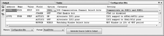
Here’s a snippet of the source code produced by generating code:
// FPOR
#pragma config ALTI2C1 = ON    // Alternate I2C1 pins (I2C1 mapped to
                               //   ASDA1/ASCL1 pins)
#pragma config ALTI2C2 = OFF   // Alternate I2C2 pins (I2C2 mapped to SDA2/SCL2
                               //   pins)
The #pragma statement provides a mechanism for introducing compiler-specific information, which is the configuration bit settings. Here, ALTI2C1 specifies which pins (SDA1/SCL1 or ASDA1/ASCL1) the I2C serial interface is mapped to (Chapter 10 discusses the I2C serial interface); in the previous example, they are mapped to the ASDS1/ASCL1 pins. Similar logic applies to the ALTI2C2. When puzzled about a configuration bit setting, consult the additional information provided in the configuration bit description in [27]. A complete list of the configuration bits and their functions is also found within [27]. Other members of the PIC24/dsPIC33 family have many of the same configuration bit capabilities as the dsPIC33E family, but the configuration register names and bit locations differ.
Clock Generation
The PIC24 family supports a wide array of clocking options [15]; this datasheet provides a complete reference. To summarize the most common options, the processor can be operated from:
![]() An internal clock source, named the fast RC oscillator (FRC), provides a convenient but less accurate time base.
An internal clock source, named the fast RC oscillator (FRC), provides a convenient but less accurate time base.
![]() An externally-supplied crystal, termed a primary oscillator, provides an accurate time base. The crystal must be connected between the OSC1 and OSC2 pins along with the two capacitors as shown; a typical value for the capacitors is 15 pF. See the application note in reference [43] for more information on capacitor selection.
An externally-supplied crystal, termed a primary oscillator, provides an accurate time base. The crystal must be connected between the OSC1 and OSC2 pins along with the two capacitors as shown; a typical value for the capacitors is 15 pF. See the application note in reference [43] for more information on capacitor selection.
![]() Several other options, such as a 32.768 KHz watch crystal or a low-power RC oscillator (LPRC).
Several other options, such as a 32.768 KHz watch crystal or a low-power RC oscillator (LPRC).
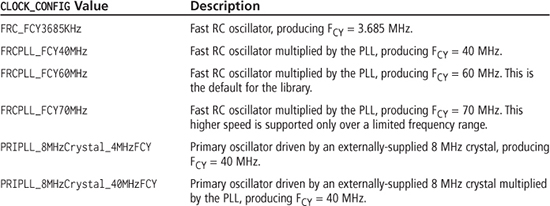
This base frequency can then be modified using either a phase-locked loop, an analog circuit which can multiply the clock frequency, or dividers to produce the desired operating frequency for the processor. Again, consult the datasheet for details. The library accompanying the book provides the following options; choose one by selecting Run > Set project configuration > Customize from the main menu, selecting xc16-gcc from the Categories tree, selecting Preprocessing and messages from the option categories drop-down box, clicking on the table cell to the left of Define C macros, then entering CLOCK_CONFIG=value, where value is chosen from Table 8.1. For example, entering CLOCK_CONFIG=FRCPLL_FCY40MHz selects a 40 MHz clock. See libincludepic24_clockfreq.h for further details; additional options can be added with relative ease by following the instructions given there.
The choice of clock changes the contents of the configClock() function, which must be called by main() to select the desired operating clock.
Table 8.1: dsPIC33E Clocking Options
Power-On Reset Behavior and Reset Sources
You have already read three causes of processor reset [16], namely the reset instruction, power-on reset (POR), and a low-true assertion of the MCLR# input. Figure 8.10 shows the complete set of processor reset sources. Brown-out reset (BOR) occurs when the input VDD drops below the level required for maintaining an operating core voltage. Both BOR and POR trigger operation of the power-on reset timer (PWRT), which delays the release of the SYSRST# signal until the input VDD has time to settle. Once SYSRST# is released, the power-on reset clock source is started and after this is detected as stabilized, the system transitions from the reset state to the running state.
A trap conflict reset occurs if a lower priority hard trap occurs when a higher priority trap is being processed; this is discussed further in Chapter 9. An illegal opcode reset occurs if the instruction that is fetched contains an illegal opcode. An uninitialized W register reset occurs if a W register is used in an indirect addressing mode before being written with a value. The integrity of the configuration information within peripheral pin select registers is monitored by maintaining copies in shadow registers; if a difference between the shadow registers and pin select registers is detected then a configuration mismatch reset is generated. Attempts to execute protected blocks of code on the chip trigger a security reset. Resets related to the watchdog timer (WDT) and sleep/idle power modes are discussed in the next section.
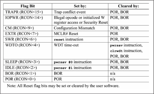
Figure 8.11 shows the RCON register bits that reflect the source of a processor reset. These can be used to debug a system that is experiencing intermittent reset. It is important that the user application clears these bits between resets or else a previous reset condition will mask the source of the current reset.
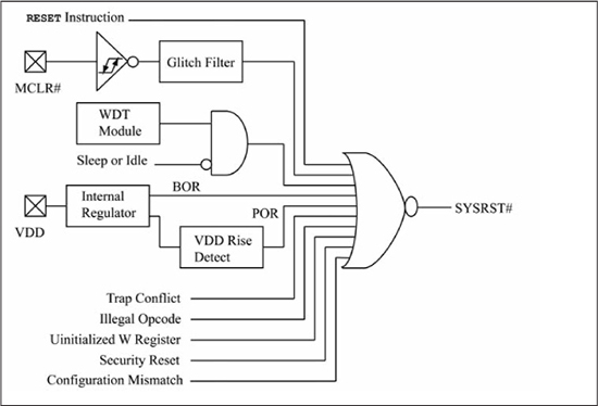
Source: Figure redrawn by author from Figure 8.1 found in the dsPIC33E/PIC24E Family Reference Manual, section 8: reset (DS70602B), Microchip, Technology Inc.
Figure 8.11
RCON register bit operation
Source: Figure redrawn by author from Table 8.2 found in the dsPIC33E/PIC24E Family Reference Manual, section 8: reset (DS70602B), Microchip Technology Inc.
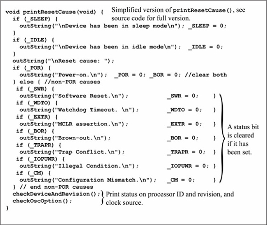
Figure 8.12 shows the code for the printResetCause() function called by echo.c in Figure 8.6 (for space reasons, this a simplified version of printResetCause(); the full code is contained in libsrcpic24_util.c). Observe that printResetCause() checks each RCON register status bit, outputs an appropriate status message if the bit is set, then clears the bit. At the end of printResetCause(), the checkDeviceandRevision() function prints the processor ID and revision and checkOscOption() function prints a status message about the current clock option.
Figure 8.12printResetCause() function
Watchdog Timer, Sleep, Idle, and Doze
Figure 8.13 shows the block diagram of the watchdog timer (WDT) subsystem [17] mentioned previously. A timer is simply an N-bit counter; when N counts have passed the amount of time is equal to N * TTMR, where TTMR is the period of the clock signal that drives the counter. When the counter’s value wraps from its maximum value back to 0, the timer is said to have expired. A timer’s timeout value can be lengthened by having a programmable prescaler to divide the input clock frequency, and/or by having a programmable output postscaler that accumulates multiple counter rollovers as one timer expiration event.
The WDT is clocked by the LPRC oscillator. The timeout period for the WDT is affected by its prescaler and postscaler settings, both of which are set by configuration bits. The prescaler can either be a fixed divide-by-32 or divide-by-128, while the postscaler is controlled by a 4-bit field that gives settings of 1:1, 1:2, 1:4, 1:8, ... up to 1:32,768.
Figure 8.13
Watchdog timer block diagram
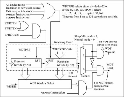
Source: Figure redrawn by author from Figure 9.2 found in the dsPIC33E/PIC24E Family Reference Manual, section 9: watchdog timer (DS70615C), Microchip Technology Inc.
A common use of the watchdog timer is for catching coding errors during development where a programmer uses an incorrect code sequence for communicating with an external device, and an expected response from the device does not occur, resulting in an infinite wait condition. Enabling the watchdog timer during the wait for the response places a maximum time limit on the wait before a watchdog timer reset occurs. In production code, the watchdog timer can protect against an infinite wait condition in case noise or hardware failure corrupts communication with an external device. It is useful to think of the watchdog timer as an alarm clock in these scenarios, signaling that too much time has elapsed. Checking the WDTO (watchdog timer timeout) bit after a reset detects when this situation has occurred. To prevent WDT timeout during normal operation, the PIC24 instruction clrwdt (clear watchdog timer, which has no arguments) must be executed periodically to reset the WDT before the WDT expires. The optional windowed mode of the WDT is enabled by the WINDIS configuration bit. In windowed mode, the WDT can only be cleared in the last 25 percent of its timer operation, or else the processor is reset. This places both minimum and maximum bounds when timing an operation, and thus provides processor reset in the case that an event requires too little time or too much time.
The WDT operation is enabled by either the FWDTEN configuration bit or the SWDTEN bit contained in the RCON register (RCON<5>). The FWDTEN bit forces the WDT to be always enabled, while the SWDTEN bit gives the application control over WDT enabling. The following lines are used in libsrcpic24_configbits.c to configure the WDT:
#pragma config WDTWIN = WIN25      // Watchdog Window Select bits (WDT Window
                                   // is 25% of WDT period)

// FWDT
#pragma config WDTPOST = PS512     // Watchdog Timer Postscaler bits (1:512)
#pragma config WDTPRE = PR128      // Watchdog Timer Prescaler bit (1:128)
#pragma config WINDIS = OFF        // Watchdog Timer Window Enable bit
                                   // (Watchdog Timer in Non-Window mode)
#pragma config FWDTEN = OFF        // Watchdog Timer Enable bit (Watchdog timer
                                   // enabled/disabled by user software)
These configuration bits allow software control of the watchdog timer (FWDTEN = OFF), disable windowed mode (WINDIS = OFF), and set the prescaler to divide-by-128 (WDTPRE = PR128) and the postscaler to 1:512 (WDTPOST = PS512). Using the nominal LPRC clock frequency of 32.768 kHz, this provides a timeout value of:
The other use of the WDT is to wake the processor from either idle or sleep mode, which are two power conservation modes [17]. Sleep mode is entered by executing the pwrsav #0 instruction, which disables the system clock and all on-chip peripherals that depend on it. Idle mode (pwrsav #1) disables the CPU, but the system clock continues to operate; peripherals must be disabled manually through their associated control registers if desired. Sleep mode is the lowest power mode available to the PIC24. When the CPU is disabled by entering either sleep or idle modes, the watchdog timer continues to operate (if enabled). If the WDT expires during idle/sleep mode, then a WDT wakeup occurs and the processor continues execution at the instruction following the pwrsav instruction. An enabled interrupt event (Chapter 9) can also wake the processor from sleep/idle mode.
Why does entering sleep mode decrease power consumption? The answer is straightforward: if the clock is stopped, no transistors are switching, which means no energy is being dissipated, thus reducing power. Of course, some energy is being dissipated, even with the clock stopped, but the amount is much lower than with the clock running. Power dissipation in a CMOS circuit is divided into two categories: static (Ps) and dynamic (Pd). Static power is the power dissipated when no switching activity is occurring and is due to high-resistance leakage paths between VDD and ground within CMOS transistors. Power dissipation is measured in watts (1 Watt = 1 Volt * 1 Amp), but in datasheets, power dissipation is typically given as power supply current for a particular operating condition. The dsPIC33EP128GP502 typical sleep mode current at room temperature as listed in the datasheet is approximately 35 μA, and the idle current is 20 mA @ FCY = 70 MHz. The idle current is much higher than the sleep current because the main system clock is being used to drive the peripheral subsystems. The principal contribution to dynamic power dissipation Pd is given in Equation 8.2, where VDD is the power supply voltage, f the switching frequency, and c the amount of capacitance being switched.
Because power is voltage multiplied by current (V • I), replacing Pd with VDD • I in Equation 8.2 yields:
By Equation 8.4, you can see that there is a linear relationship between I, VDD, frequency, and capacitance. Idle mode reduces the capacitance c being switched, because the CPU operation is disabled and thus fewer transistors are switching, but the clock frequency remains unchanged and is still driving the peripheral modules. Sleep mode sets frequency for the system clock to zero, since the system clock is disabled.
The doze postscaler, a component of the system clock module, is another method for reducing power. The doze postscaler reduces the system clock frequency to the CPU, but keeps the system clock frequency to the rest of the peripherals unchanged. This means that timing-sensitive modules such as the UART that you use for serial communication to PC will continue to function at the same data rate, and thus the baud rate for the serial link can remain unchanged. If the system clock frequency for peripherals was also reduced, then the baud rate for the UART would also have to be reduced since the serial communication rate is derived from the system clock. If the doze postscaler is set to a 1:2 setting, which reduces the CPU clock frequency by a factor of 2, then the current drawn by the CPU portion of the PIC24 will also be reduced by one half, assuming that the static power contribution from the CPU (non-switching current draw) is small. On the dsPIC33E, static current draw is in the 10s of microamperes, as reported by the datasheet for the sleep mode current.
The reset.c Test Program
A program named reset.c is used in this section to illustrate the concepts of persistent variables, sleep/idle mode, watchdog timer reset, watchdog timer wakeup, and doze mode. Figure 8.14 shows the portion of reset.c before entry into the program’s infinite while (1) loop. The configuration code executed before the outString(HELLO_MSG) statement is the same as for Figure 8.6 (echo.c) with one addition, the configPinsForLowPower() function that configures all of the parallel I/O pins for low-power operation (which configures all unused pins as inputs with weak pull-ups enabled; see the next section for details), powers off unused peripherals, and disables the internal voltage regulator when in sleep mode. The function is used here because you need to measure the current draw for various power modes and want the parallel I/O pins and other peripherals configured for the least possible current draw.
Figure 8.14chap08
eset.c: Setup portion of program
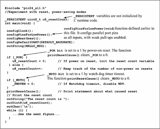
The _PERSISTENT uint8_t u8_resetCount declaration means that the u8_resetCount variable is never initialized by the C run-time code. This allows the variable to track events across processor resets; in this case it’s used as a simple counter for the number of non-POR events that occur. Observe that u8_resetCount is initialized to 0 only when the _POR bit is set, indicating that a power-on reset has occurred. If the _WDTO bit is set, indicating that a watchdog timer expiration caused the last processor reset, then the _SWDTEN bit is cleared, disabling the operation of the watchdog timer. Before entering the while (1) loop, the u8_resetCount value is printed by the function outUint8(uint8_t u8_x), which prints its argument to the console in ASCII-hex. The outUint8(uint8_t u8_x) function is found in libsrcpic24_serial.c.
Figure 8.15 shows the while (1) portion of the reset.c program. The printMenuGetChoice() function (not shown) outputs a menu of choices 1–7, where the choices are:
![]() 1: Enables the WDT, which is configured for a 2-second timeout period. After the menu is reprinted, a processor reset occurs when the WDT expires if no further action is taken by the user. Recall that the WDT is disabled by the code preceding the
1: Enables the WDT, which is configured for a 2-second timeout period. After the menu is reprinted, a processor reset occurs when the WDT expires if no further action is taken by the user. Recall that the WDT is disabled by the code preceding the while (1) loop on a processor reset.
![]() 2: Enters sleep mode (
2: Enters sleep mode (pwrsav #0 instruction). Because the WDT is disabled at this point, the only way to wake up the processor with a user action is to cycle power or press the MCLR# reset button. A C inline assembly statement (asm) is used to insert the pwrsav #0 instruction into the C code.
![]() 3: Enters idle mode (
3: Enters idle mode (pwrsav #1 instruction). As with sleep mode, a power cycle or pressing the MCLR# reset button is required by the user to wake the processor.
![]() 4: Enables the WDT, then enters sleep mode. The processor will sleep for approximately 2 seconds because of the particular watchdog timer configuration bit settings, then wake when the WDT expires, reprinting the menu choice. If no further action is taken by the user, the WDT expires again in 2 seconds, causing a processor reset, then the WDT is disabled before re-entering the
4: Enables the WDT, then enters sleep mode. The processor will sleep for approximately 2 seconds because of the particular watchdog timer configuration bit settings, then wake when the WDT expires, reprinting the menu choice. If no further action is taken by the user, the WDT expires again in 2 seconds, causing a processor reset, then the WDT is disabled before re-entering the while (1) loop.
![]() 5: Enables doze mode with an FCY divided by 2. No visible change is apparent to the user, but an ammeter shows a reduction in current draw.
5: Enables doze mode with an FCY divided by 2. No visible change is apparent to the user, but an ammeter shows a reduction in current draw.
![]() 6: Enables doze mode with an FCY divided by 128. No visible change is apparent to the user, but an ammeter shows a reduction in current draw.
6: Enables doze mode with an FCY divided by 128. No visible change is apparent to the user, but an ammeter shows a reduction in current draw.
![]() 7: Executes a software reset via the
7: Executes a software reset via the reset instruction.
Figure 8.16 shows some sample output from the reset.c program for the choice sequence of 1 (enable watchdog timer) in comments a through c, followed by 2 (enter sleep mode) in comments d through g, and finally 4 (enable WDT, then enter sleep mode) in comments h through j.
Figure 8.15chap08
eset.c: while (1) portion of the reset.com program
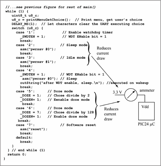
Figure 8.16
Sample output from the reset.c program
Table 8.2 shows the VDD current draw in mA as measured by an ammeter when testing the sleep, idle, doze(/2), and doze(/128) modes using the reset.c program for two different PIC24 microcontrollers.
Table 8.2: PIC24 Current Draw (mA)
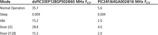
The following comments will use the numbers in Table 8.2 for the dsPIC33EP128GP502 with FCY = 60 MHz. As previously stated, the sleep mode offers the greatest reduction in current draw because it stops the system clock as well as all of the peripherals, as shown in Table 8.2 with a measured current draw of 8.8 μA. The idle mode stops the clock to the CPU, but not the clock to the peripherals, producing a 15.2 mA current draw. The doze mode of FCY/2 had a measured current draw of 28.8 mA. Because doze mode only affects the CPU clock and not the peripheral clock, you could have roughly predicted the doze mode current draw, as shown in Equation 8.5, where N is the doze mode postscaler.
Idle mode current subtracted from Normal mode current is approximately the current drawn by the CPU, which is the current that is affected by doze mode. Using values from Table 8.2 for Normal and Idle currents, Equation 8.6 predicts a doze current for FCY/2 mode of 25.5 mA, which is reasonably close to the measured value of 28.8 mA.
The PIC24F has lower maximum performance than the dsPIC33E family, but offers lower power consumption at equivalent clock frequencies. The difference in current values between the two devices in Table 8.2 is exaggerated because of the clock speed inequity.
Parallel Port Operation
Parallel port I/O, also termed general-purpose I/O (GPIO), refers to groups of pins whose values can be read or written as a group via special function registers. On the dsPIC33EP128GP502 μC, two parallel ports are available: PORTA and PORTB. Additional ports, such as PORTC, PORTD, PORTE, and higher are available on larger pin count versions of the PIC24 μC. Each port is 16 bits wide, but whether or not all ports are available on external pins depends on the particular PIC24 μC. For example, on the dsPIC33EP128GP502 all 16 bits of PORTB are available externally, but only the lower 5 bits of
PORTA are. The individual port pins on the dsPIC33EP128GP502 pin diagram in Figure 8.2 are named RBx or RAx, for PORTB and PORTA, respectively. The various parallel ports A, B, C, and so on, all operate the same in terms of their basic digital input/output functionality. Only PORTA and PORTB are used in the interfacing examples in this book, as the dsPIC33EP128GP502 μC is the target device.
Figure 8.17 shows the general diagram of a parallel port pin. Each parallel I/O (PIO) pin may share the external pin with other on-chip peripherals, labeled as Peripheral Modules in Figure 8.17. Control bits in special function registers determine which peripheral actually has access to the pin when multiple peripheral outputs share the same physical pin. This is shown conceptually in Figure 8.17 as the output multiplexer logic.
The shaded pins are 5 V tolerant—input voltages of up to 5.5 V do not damage the pin (note that this capability requires VDD ≥ 3.0 V). The remaining pins support a maximum input voltage of VDD + 0.3 V, or 3.6 V assuming that VDD is 3.3 V. Most dsPIC33E I/O pins can sink and source a maximum of 5 mA (some exceptions exist; see [31]).
Figure 8.17
Parallel port general structure
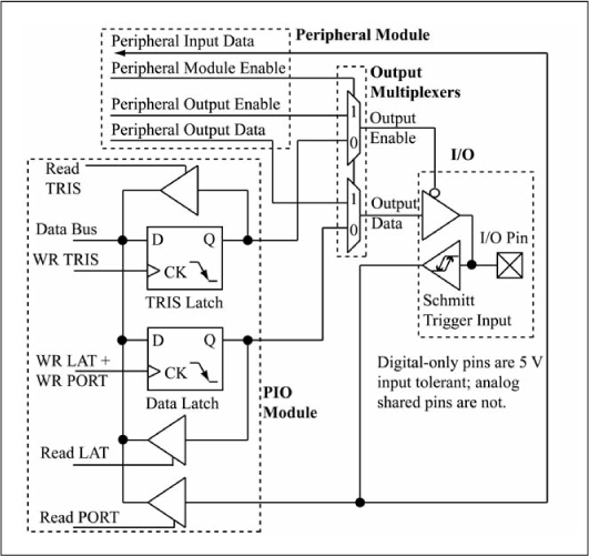
Source: Figure redrawn by author from Figure 11.1 found in the dsPICEP128GP502 datasheet (DS70000657H), Microchip Technology, Inc.
Each parallel port has three special function registers associated with it named PORTx/TRISx/LATx, where x is the specific port such as A or B. The TRIS x register is used to configure each bidirectional port bit as either an input or output. A 1 in a TRISx register bit configures the associated PORTx register bit to be an input (note that 1 looks like I for input), while a 0 configures the associated PORT x register bit to be an output (0 looks like O for output). The LATx register is the data latch used to drive the port pins when it is configured as an output. Reading PORTx returns the values of the external pins, while reading LATx reads the data latch value. Writing to either LATx or PORTx writes to the data latch of the associated port. Individual bits are referenced as LATxy and Rxy where x gives the port’s letter (A-E) and y gives the bit within the port. In C code, these references can be written as _R xy (_RA2, _RB5, _RB14, and so on) for bits in the PORTx register and as _LATxy/_TRISxy (_LATA2, _TRISB5, _LATB14, and so on) for bits in the LATx/TRISx registers. Generally, the code examples use individual bit assignments instead of assigning all bits of a port at once. Note that reading _LATxy may not return the same value as reading _Rxy. If the port is configured as an input, reading _LATxy returns the last value written to _LATxy or _Rxy, while reading _Rxy returns the value of the external pin. If the port is configured as an output, reading _LATxy will normally return the same value as reading _Rxy because the data latch is driving the external pin. However, if there is another external driver that is clashing with the port driver, or if the port driver itself is a special case like an open-drain output (explained later in this section), _LATxy and _Rxy may return different values when read. A write to a port bit configured as an input changes the value of the output data latch (_LATxy), but does not change the value seen on the external pin whose value is set by whatever is driving that pin. Even though in principle writing to _Rxy is equivalent to writing to _LATxy, in the case of bset (bit set) or bclr (bit clear) instructions they are not equivalent because these are read-modify-write instructions. Thus, a bit set of _Rxy reads _Rxy, modifies the value, then writes _Rxy, while a bit set of _LATxy reads _LATxy, modifies the value, then writes _LATxy. The Family Reference Manual [18] warns that the following consecutive assignments
_RB2 = 1;     // Implemented by compiler using a bset instruction
_RB3 = 1;     // Implemented by compiler using a bset instruction
can produce an incorrect result for the second assignment (even though they are for different bits), depending on external pin loading and internal clock speed. However, using _LATxy for port writes always works:
_LATB2 = 1;     // Implemented by compiler using a bset instruction
_LATB3 = 1;     // Implemented by compiler using a bset instruction
Because of this, the code uses _LATxy for port writes, and _RBxy for sensing (reading) a pin state. The code reads _LATxy when you want to toggle a previously written value, such as _LATB2 = !_LATB2.
Tristate Drivers
Figure 8.18 shows that the output of a _TRISx latch bit y (_TRISxy) is connected to the output enable of the tristate buffer that drives the I/O pin. If _TRISxy is 0 (the port bit is an output), the tristate buffer is enabled and simply passes its input value to its output. If _TRISxy is 1 (the port bit is an input), the tristate buffer is disabled, and its output becomes high impedance, whose state is commonly designated as Z. Figure 8.18 shows that you can think of the tristate buffer enable as controlling a switch on the output of the buffer; the switch is closed when the enable is asserted, allowing the buffer to drive its output. The switch is open when the enable is negated, causing the output to float (also known as high impedance). Note that a port bit cannot be both an input and an output simultaneously; it is either one or the other based on the setting of the _TRISxy bit. The lower part of Figure 8.18 shows data flow on a bidirectional data link using one wire; data is either flowing from CPU_a to CPU_b or vice versa, but never both directions at the same time over one wire if voltage mode signaling is used (if both tristate buffers are enabled then this can cause an indeterminate voltage on the wire and it is a programming error in the μC application).
Figure 8.18
Tristate buffer operation and bidirectional I/O
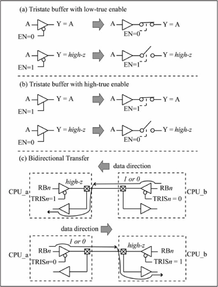
Schmitt Trigger Input
All PIO inputs use a Schmitt Trigger input buffer for driving internal signals from the external pin. Figure 8.19 shows the Vin/Vout characteristics of a Schmitt Trigger buffer. Observe that a low-to-high transition must become close to VDD (VIH) before the buffer trips; conversely, a high-to-low transition must be close to ground (VIL) before the buffer trips. This hysteresis in the buffer action provides extra immunity against noise on the input signal and is also used for transforming slowly changing inputs into signals with fast rise and fall times.
Figure 8.19
Schmitt Trigger input buffer characteristic
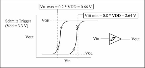
Open-Drain Output
Many PIO pins have the capability to be configured as an open-drain driver, which means that the PMOS pull-up is disabled, as shown in Figure 8.20(b), removing the ability of the port pin to drive its output high (instead, the output pin floats when driven high). One application of an open-drain driver is to use an external pull-up resistor to provide an output high voltage that is higher than the PIC24 VDD value of 3.3 V. In the case of Figure 8.20(c), the external pull-up is used to provide an output voltage of 5 V. The value of the pull-up resistor is chosen so that the current sunk by the pin when the output is pulled low does not exceed the maximum current specification, which is 5 mA for the majority of the dsPIC33E I/O pins. Thus, the resistor value should be at least 5 V/.005 A = 200 Ω. Another open-drain application is shown in Figure 8.20(d), in which two open-drain outputs are connected together to form a wired logic function. This is a common usage when wanting to detect if any of the outputs are asserted low (a low-true OR function); the outputs can simply be wired together with an external pull-up without the need for a logic gate. The maximum allowed open-drain voltage for a pin is the same as the pin’s maximum allowed VIH (5.6 V for digital pins) as per the datasheet [31].
Figure 8.20
Open-drain driver and application
Most PIO ports have an open-drain control register (ODCx) that is used for enabling (_ODCxy = 1) or disabling (_ODCxy = 0) the open-drain capability. The following two C statements configure port RB11 as an open-drain output:
_TRISB11 = 0;   // RB11 is an output.
_ODCB11 = 1;    // RB11 output is open-drain.
Internal Weak Pull-Ups and Pull-Downs
Most I/Os have a capability referred to as input change notification. These pins have a weak pull-up that can be enabled (_CNPUxy = 1) or disabled (_CNPUxy = 0), as well as a weak pull-down that can be enabled (_CNPDxy = 1) or disabled (_CNPDxy = 0), as shown in Figure 8.21(a). The term weak is used because the resistance is high enough that an external driver can overpower the pull-up resistor and pull the input to near ground, producing a 0 input. The weak pull-up is implemented as a high-resistance P-transistor and when enabled, the gate of this transistor is 0, turning it on. Similar statements apply to pull-downs. The weak pull-up is useful for eliminating the need for an external pull-up resistor on an input switch, as shown in Figure 8.21(b). If an external device providing input sometimes enters a high-impedance state, by driving its output neither high nor low, a weak pulldown could be used to produce a known value of 0 at the input to the μC. Note that a pushbutton switch configured as a low-true input switch must have some form of pull-up resistor, either internal or external, or the input floats when the pushbutton is not pressed, allowing the input to be read as either 1 or 0.
Figure 8.21
Change notification weak pull-ups
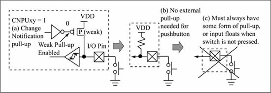
The following two C statements configure RB11 as an input, then enable the weak pull-up on that pin.
_TRISB11 = 1;   // RB11 is an input.
_CNPUB11 = 1;   // Enable weak pull-up on RB11.
Digital versus Analog Inputs
One of the peripherals that shares a physical pin with the PIO module is the analog-to-digital converter (ADC) module. ADC inputs are labeled as ANn on the dsPIC33EP128GP502 pin diagram in Figure 8.2, so it is seen that RB3 is assigned the same physical pin (7) as analog input AN5. An additional complication is that in order for the parallel port to be used as an input, the analog functionality of the pin has to be disabled, which can be done using the _ANSELxy bit associated with each ANn input (the older PIC24H family used a register named PCFG for the same purpose). By default, each I/O with an ANn function is configured as an analog input (_ANSELxy = 1), but it can be configured for digital mode by clearing the _ANSELxy bit (_ANSELxy = 0). For example, RB3 shares pin 7 with AN5, so the following two C statements configure RB3 as an input:
_TRISB3 = 1;   // RB3 is an input.
_ANSELB3 = 1;  // Configure RB3 (AN5) for digital mode.
A PIO pin configured as an input, but with the analog mode enabled, will always read as 0. As suggested by the PIC24 Family Reference Manual, you will also configure a pin for digital mode when a PIO is used as an output so that the analog input circuitry does not load the output driver (this load is significant and slows signal transitions).
PIO Control Bits Summary
Table 8.3 summarizes the control bits used to configure parallel I/O for a single pin of a PIC24 device.
PIO Configuration Macros/Functions
Because of the numerous options available for PIO pins (input/output, analog/digital, weak pull-up/pull-down, open-drain), you can use macros for PIO configuration to improve code clarity. These macros are contained in libincludepic24_ports.h and are:
![]() Pull-up/pull-down configuration: These enable/disable the weak pull-ups/pull-downs on
Pull-up/pull-down configuration: These enable/disable the weak pull-ups/pull-downs on PORTA/PORTB pins and are named ENABLE_Rxy_PULLUP(), DISABLE_Rxy_PULLUP(), ENABLE_Rxy_PULLDOWN(), and DISABLE_Rxy_PULLDOWN(), where x = A for port A or B for port B and y gives the bit number on that port; for example, xy = B5 refers to RB5. For the dsPIC33EP128GP502, all PIO pins have an associated input change notification functionality, so all have the weak pull-up capability and pull-down (this is not true for all PIC24 microcontrollers).
![]() Open-drain configuration: These enable/disable the open-drain functionality on
Open-drain configuration: These enable/disable the open-drain functionality on PORTA/PORTB pins and are named ENABLE_Rxy_OPENDRAIN() and DISABLE_Rxy_OPENDRAIN().
![]() Input/output configuration: These configure the
Input/output configuration: These configure the PORTA/PORTB pins as either inputs or outputs and are named CONFIG_Rxy_AS_DIG_INPUT()and CONFIG_Rxy_AS_DIG_OUTPUT(). The input macros disable the weak pull-up/pull-down and configure analog pins for digital mode as necessary. The output macros disable the weak pull-up/pull-down and also the open-drain capability.
The libincludepic24_ports_config.h file includes device-specific macros based on the target device set within MPLAB®. The following code shows simplified examples of the input/output configuration functions for the RA0 pin:
// Low-level config
//
// Analog:

/// Enable analog functionality on pin RA0.
#define ENABLE_RA0_ANALOG()  (_ANSA0 = 1)
/// Disable analog functionality on pin RA0.
#define DISABLE_RA0_ANALOG() (_ANSA0 = 0)

// Input/output:
/// Configure pin RA0 as an input.
#define CONFIG_RA0_AS_INPUT()  (_TRISA0 = 1)
/// Configure pin RA0 as an output.
#define CONFIG_RA0_AS_OUTPUT() (_TRISA0 = 0)

// Open-drain:
/// Enable the open-drain driver on pin RA0.
#define ENABLE_RA0_OPENDRAIN()  (_ODCA0 = 1)
/// Disable the open-drain driver on pin RA0.
#define DISABLE_RA0_OPENDRAIN() (_ODCA0 = 0)

// Change notification, pull-ups and pull-downs:
/// Enable the pull-up on pin RA0.
#define ENABLE_RA0_PULLUP()  (_CNPUA0 = 1)
/// Disable the pull-up on pin RA0.
#define DISABLE_RA0_PULLUP() (_CNPUA0 = 0)

/// Enable the pull-down on pin RA0.
#define ENABLE_RA0_PULLDOWN()  (_CNPDA0 = 1)
/// Disable the pull-down on pin RA0.
#define DISABLE_RA0_PULLDOWN() (_CNPDA0 = 0)

// High-level config
//        -
void CONFIG_RA0_AS_DIG_INPUT() {
  DISABLE_RA0_ANALOG();
  CONFIG_RA0_AS_INPUT();
  DISABLE_RA0_OPENDRAIN();
  DISABLE_RA0_PULLUP();
  DISABLE_RA0_PULLDOWN();
}

void CONFIG_RA0_AS_DIG_OUTPUT() {
  DISABLE_RA0_ANALOG();
  CONFIG_RA0_AS_OUTPUT();

  DISABLE_RA0_OPENDRAIN();
  DISABLE_RA0_PULLUP();
  DISABLE_RA0_PULLDOWN();
}
The low-level configuration macros provide a meaningful name for the PIO control bits discussed previously. The more convenient high-level configuration functions configure a pin in the most common states (as a digital input or output); for finer control, follow a high-level configuration with a low-level configuration:
CONFIG_RA0_AS_OUTPUT();
ENABLE_RA0_OPENDRAIN();
Not all pins provide all the functionality shown previously. For example, RA2 lacks analog capability. In this case, the ENABLE_RA2_ANALOG() macro is not defined, while DISABLE_RA2_ANALOG() does exist, but does nothing.
When configuring many I/O ports, it is more code efficient to directly write 16-bit values to configuration registers such as _TRISx, _ANSELx, and so on. However, I will sacrifice some code efficiency for code clarity in the examples by use of these macros since this is an introductory text on microcontroller interfacing, so code clarity is more important at this point.
LED/Switch I/O and State Machine Programming
A common input device is a momentary pushbutton switch. Figure 8.22 shows a pushbutton switch connected to RB13, with RB13 configured as an input with the weak pull-up enabled. When the pushbutton is released (not pressed) the RB13 input reads as 1; when the pushbutton is pressed the RB13 input reads as 0. Port RB14 is configured as a digital output for driving an LED, which has a 470 Ω series resistor. To compute the needed resistance value, recall that a typical PIO pin on the PIC24 μC can provide a maximum current of 5 mA, and so you can use this value as the target current through the LED in order to maximize the LED illumination. Next, consult the LED’s datasheet to determine the voltage drop across the LED at the selected current; a typical figure for many LEDs is 2 V. Recalling that Ohm’s law is V = IR, solving for resistance gives R = V/I, where V is the voltage drop across the resistor. With a 3.3 V supply and a 2 V drop across the LED, this leaves V = 3.3 – 2 = 1.3 V. Therefore, the resistance R = 1.3 V/0.015 A = 260 Ω, which gives the lowest resistance allowed for a 5 mA or less target current. Older PIC24 variants such as the PIC24H supply only 4 mA; to support this family as well and to add some margin of safety, a value of 470 Ω was chosen. The CONFIG_LED1() macro is used for configuring the port that drives the LED, while the config_pb() function is used for configuring the input port used for the switch. In general, macros will be used for single-line statements while functions will contain multi-line routines. Observe that the RB13 pull-up is enabled in config_pb() after the port is configured as a digital input. The PB_PRESSED() and PB_RELEASED() macros are used for testing if the switch is pressed or released, respectively.
In both the (a) and (b) code segments, a 1 μs delay (DELAY_US(1)) is used after configuring SW1 to allow the pull-up on the port to work. After enabling a pull-up, the PIC24 μC with a fast clock can read an input port before the input has had time to be pulled to a logic 1, so the code examples use this conservative delay after enabling weak pull-ups on input ports.
Figure 8.22
Toggling an LED after a switch press and release
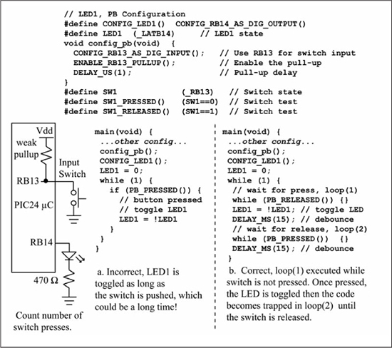
Assume that you would like to toggle the LED each time the pushbutton is pressed and released (toggle means to turn the LED off if it is currently on, and vice-versa). A common mistake is shown in code segment (a), which toggles the LED when the switch is pressed (RB13 returns 0). The problem with this code is that the LED is not only toggled when the pushbutton is pressed, but is also toggled for as long as the pushbutton is held down. Human reaction times on pushbutton switches are measured in tens of milliseconds, so the LED is toggled many times for each pushbutton activation! Code segment (b) shows a correct solution to this problem. When the while (1) loop is entered, the code becomes trapped in the loop while (PB_RELEASED), which loops waiting for the pushbutton to be pressed. Once the pushbutton is pressed, the LED is toggled and code is then trapped in the loop while (SW1_PRESSED), waiting for the pushbutton to be released. Upon release, the code becomes trapped in the loop while (SW1_RELEASED) again. Thus, the LED is toggled only once for each press and release of the pushbutton. Moving the toggle statement (LED1 = !LED1) to the end of the outer while (1) loop toggles the LED when the pushbutton is released, but the end result of toggling once for each press and release remains the same. The DELAY_MS(15) function calls are included after each change in the input switch status to ensure that all switch bounce has settled before continuing. Mechanical switch bounce can produce multiple pulses when a pushbutton is activated. The required delay is a function of the mechanics of the switch bounce, which can only be seen by using an oscilloscope to capture the switch waveform or from a manufacturer datasheet. The value of 15 ms used here should be adequate for common momentary switches. This is a simple method for debouncing a switch with the drawback that the CPU cycles spent in the software delay loop are wasted. Alternative methods for switch debouncing are presented in Chapter 9.
State Machine I/O Programming
The code of Figure 8.22(b) waits for an I/O event (switch press and release) then performs an action (LED toggle). A common task in microcontroller applications is to perform a sequence of events that spans a series of I/O actions. A finite state machine (FSM) approach for code structure is useful for these types of problems. Figure 8.23 shows the LED toggle problem of Figure 8.22 cast as a state machine specification.
Figure 8.23
State machine specification of LED toggle problem
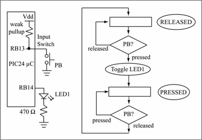
The state machine consists of two states, named PRESSED and RELEASED, matching the state of the pushbutton. The RELEASED state progresses to the PRESSED state when PB is pressed, toggling the LED during the transition. This is a conditional state output, because the output only occurs if a specific condition (here, the pushbutton being pressed) is true. The PRESSED state moves to the RELEASED state when PB is released. Specifying I/O actions as a state machine is common practice because the state machine is a non-ambiguous description.
Figure 8.24 shows a code implementation for the LED toggle problem written in a state machine style. This style will be the preferred method for I/O problems. Although more verbose than Figure 8.22, it allows us to code complex I/O problems in a structured manner. The state names are defined using an enumerated type definition in Figure 8.24 (a) called STATE. An enumerated type provides for readable state names that improves code clarity. Each state name is assigned an integer value (incrementing up from the integer assigned to the first state, which is 0). Enumerated type variables are mapped to the int type in C. Next, a printable version of each state is defined in an array of strings named apsz_state_names. The print_state function outputs these strings when the state passed to it differs from the last state it was passed. The update_state function stores the current state in e_state and updates it based on the state machine shown in the previous figure. Finally, main initializes the hardware then repeatedly calls update_state, waiting 15 ms between calls to suppress switch bounce.
At the top of the while (1) loop, the print_state(e_state) function call prints the current state name to the console if the e_state value has changed since the last call. This is useful for debugging, as the current state name is needed to determine what code is being executed.
The state diagram of Figure 8.23 is implemented in update_state; the remainder of the program supports the execution of this state machine. In this function, switch (e_state) identifies the current state; specifically, each case statement maps to a state of Figure 8.23. The default state is entered whenever the switch variable does not match any of the previous case statements. It is considered good programming practice to always include a default statement in the event that the switch variable contains an unexpected value either through a programming error or some kind of memory corruption. Observe that the e_state variable is only changed if the condition for a state change is met, such as the pushbutton switch being pressed (e) in STATE_RELEASED or released in STATE_PRESSED. Because if statements are used to check conditions, rather than while statements as in Figure 8.22, the code is continually looping through the switch statement. This allows you to place a doHeartbeat() call (i) at the end of the while (1) loop to keep the heartbeat LED pulsing, giving us a visual indication that code is being executed. Switch debounce (h) is accomplished by the DELAY_MS(DEBOUNCE_DLY) at the end of the switch statement, which means that the switch input is only being checked every DEBOUNCE_DLY milliseconds (the DEBOUNCE_DLY macro is defined in libinclude pic24_delay.h and has a value of 15). This is satisfactory since the while (1) loop has no other work to do except to sample the switch. If other work was to be performed, and you did not want to have the DEBOUNCE_DLY delay each time through the while (1) loop, then the DELAY_MS(DEBOUNCE_DLY) could be placed at each point in the code where a switch change is detected, as was done in Figure 8.22(b).
Figure 8.24chap08ledtoggle.c. State machine code solution for LED toggle problem
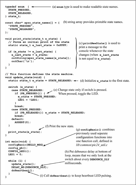
Extended State in a More Complex LED/Switch I/O Problem
In the previous problem, the state machine shown required only two states, PRESSED and RELEASED. However, the machine passes through four states: pressed and released when the LED is on, then pressed and released again when the LED is off. This is accomplished by storing one bit of state in the LED1 variable (on and off). This variable extends the effective states of the machine, transforming the two states of PRESSED and RELEASED into four states, which could be named ON_PRESSED, ON_RELEASED, OFF_PRESSED, and OFF_RELEASED. This extended state can be used to provide a state machine with complex behavior while limiting the number formal states to a manageably small set.
For example, Figure 8.25 shows a state machine specification of a more complex LED/switch I/O problem. The LED is turned off initially. After a pushbutton press and release, the LED is turned on. A slide switch input (SW) is used to control what happens after the next pushbutton press: either branch back to the initial state or continue on to a blinking state. The LED is blinked (toggled) up to five times, as long as the pushbutton is released, then the state machine returns to its initial state. Pressing the pushbutton terminates the blinking and transitions to a final state, which returns to the initial state once the pushbutton is released. The SW input is a slide switch that connects the associated port to either GND or leaves it floating, with the internal pull-up providing a logic high when the input is floating.
Figure 8.26 shows the C code implementation of Figure 8.25 in the same style as Figure 8.24. Notice that the LED is turned on and off using an unconditional state assignment – it appears without any qualifying if clause. In contrast, the extended state variable u16_led_toggles is initialized to 0 on exiting the PRESSED2 state and transitioning to the RELEASED3_BLINK state using a conditional state assignment. The remainder of the extended state usage occurs in the RELEASED3_BLINK state; in this case clause, u16_led_toggles is unconditionally incremented with each LED toggle; when this reaches 10 (which is 5 blinks), the machine moves to the initial state; if the button is pressed before 5 blinks, it moves to the PRESSED3 state.
Note that in contrast to typical programming practice, a for loop was not—and should not be—used. First, consider the following equivalent code. (Yes, C does provide a goto statement.) One of the three transitions in the state machine (a transition back to the current state) no longer appears; the other two transitions are less clearly stated, making the code harder to maintain. Second, the nature of a for loop, which traps execution inside itself, prevents this code from working in an interrupt-driven context as presented in Chapter 9, significantly limiting its usefulness. Therefore, avoid loops such as for and while and allow control to pass straight through each case statement.
case STATE_RELEASED3_BLINK:
  for (u16_led_toggles = 0; u16_led_toggles < 10; u16_led_toggles++) {
    LED1 = !LED1;
    DELAY_MS(250);

  if (PB_PRESSED()) {
    e_state = STATE_PRESSED3;
    goto exit_case;
  }
}
e_state = STATE_RELEASED1;
LED1 = 0;
exit_case:
break;
Figure 8.25
State machine specification for LED/switch I/O problem
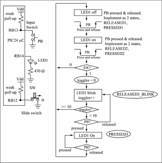
Figure 8.26chap08ledsw1.c. Code implementation for LED/switch I/O problem
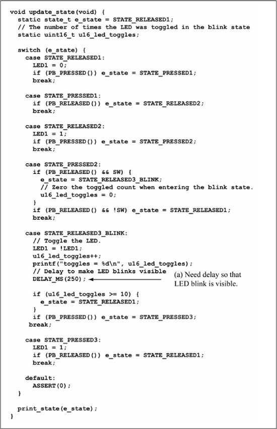
Press/release macros are not defined for SW because you are simply checking if the input is a 1 or a 0 (a) as you are not associating a press/release connotation with this input. The DELAY_MS(250) call (b) in state RELEASE3_BLINK provides a delay after toggling the LED; this is needed to ensure that the blinking action is visible. Note that while the DELAY_MS() software delay is executing, the switch input is not being sampled, which means that a very fast press and release could be missed. Chapter 9 discusses alternative methods for switch sampling that avoid this problem.
Figure 8.27
Console output for LED/switch I/O implementation
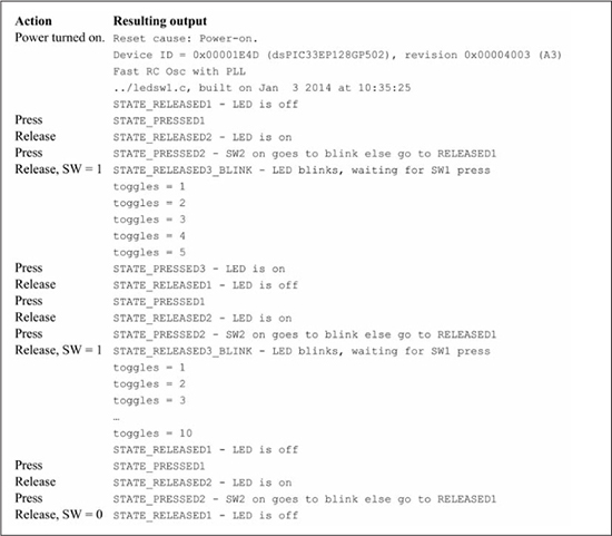
Figure 8.27 shows console output while testing the C code of Figure 8.26. The SW input was 1 for the first two times that the WAIT_FOR_RELEASE2 state was exited, causing the next state to be BLINK. After this, the SW input was 0 the next two times that the WAIT_FOR_RELEASE2 state was exited, causing the following state to be WAIT_FOR_PRESS1.
Interfacing to an LCD Module
A liquid crystal display (LCD) is often used in microcontroller applications because they are low power and can display both alphanumeric characters and graphics. Disadvantages of LCDs are that they have low viewing angles, are more expensive than LED displays, and must be lit by either ambient light or a back light. LCD character modules display multiple characters, with modules using a k x n designation where k is the number of characters displayed on each of the n display lines. LCD modules have either a parallel or serial interface, with many LCD parallel interfaces standardized around the Hitachi HD44780 LCD controller. Figure 8.28 shows a PIC24 μC to LCD interface for a Hantronix 16x2 LCD module (part# HDM16216L-5). This interface is independent of the k x n organization of the LCD module, and is applicable for most LCD modules based on the HD44780 LCD controller.
Figure 8.28
PIC24 μC to LCD interface (4-bit mode)
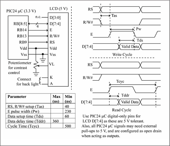
The interface is divided into control lines (E, R/W#, RS), data lines (D7:D0), and power (VDD, VSS, VL, K, A). The 4-bit interface mode is used to reduce the number of connections between the PIC24 μC and the LCD. In 4-bit mode, 8-bit data is sent in two 4-bit transfers on lines D7:D4, allowing D3:D0 to be unconnected. The K, A inputs are for the back light display (see datasheet [33]), while the VDD – VL voltage difference determines the intensity of the displayed numerals (connecting VL to VSS provides maximum intensity but may cause VDD – VL to exceed the maximum recommended VL value on some LCD modules). A logic high on the R/W# signal indicates a read operation; the LCD module provides data to the PIC24 μC. A logic low on R/W# is a write operation; the PIC24 μC provides data to the LCD module. The E signal is a data strobe used to signal valid data on the Dn, RS, and R/W# lines. To perform a write operation, the PIC24 μC places data on the Dn/RS signals, R/W# is driven low, and E is brought high and then low. The LCD latches the input data on the falling edge of E, so the Dn lines must satisfy the setup time Tds, while the control lines RS, R/W# are latched on the rising edge of E and must satisfy the setup time Tas. Not all timings are shown on the diagram; there are small hold times about the E edges that must be satisfied as well (see [33]; these are easily satisfied by typical microcontroller operation). To read data from the LCD, data is placed on the RS signal, R/W# is driven high, and E is brought high. After the data delay time Tddr has elapsed, valid data is ready on the Dn lines from the LCD, which can then be read by the PIC24 μC. The E signal is brought low to finish the read operation. Because software assignments are used to drive the E signal, the minimum pulse width depends on the system clock frequency. At FCY = 40 MHz, the PIC24 μC is capable of producing a pulse that violates the minimum pulse width requirement of the E signal. The example code uses software delays of 1 μs as a very conservative method of ensuring that the E signal timing requirements are met and because I/O transfer performance is not an important issue in this example. Using software assignments for driving PIO pins to accomplish data transfers instead of dedicated hardware modules that drive the pins is often referred to as bit-banging. The PIC24 μC has several dedicated hardware modules for accomplishing specialized data transfers without CPU intervention; these are covered in later chapters.
3.3 V to 5 V Interfacing
The LCD module used in Figure 8.28 requires a 5 V supply, the first time that you have dealt with 3.3 V to 5 V interfacing. Any input signals must be 5 V input tolerant, which means that PIC24 μC RBn ports used for the LCD D[7:4] pins must be 5 V tolerant. For output signals, a 3.3 V output port can drive a 5 V input port if the 5 V input port has TTL-level inputs (VIH is approximately 2.0 V). However, if the device has CMOS level inputs (VIH is approximately 3.8 V) then all signals will need weak external pull-ups (approximately 10 kΩ) and must be configured as open-drain outputs when acting as outputs. This would also mean that digital-only ports would have to be used for all signals since the maximum open-drain voltage is the same as the maximum input voltage. The Hantronix LCD module used in Figure 8.28 has TTL-level inputs, so external pull-ups are not required.
LCD Commands
A subset of the available LCD commands [34] is shown in Table 8.4. If RS = 0, the D7:D0 bits represent an LCD command that affects mode, screen, or cursor position. If RS = 1, the D7:D0 bits contain data being written to or read from the LCD data display RAM (DD RAM) in the form of an ASCII character code.
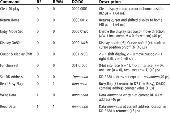
The internal memory configuration of an LCD is dependent upon the particular module. The HDM16216L-5 is a 16x2 display, but its internal data display RAM has 80 total locations with 40 locations mapped to line 1 (addresses 0x00 to 0x27) and 40 locations mapped to line 2 (addresses 0x40 to 0x67). The 16x2 display is a window into these 80 locations, with only 16 characters of each line displayed at any given time, as shown in Figure 8.29. By default, the display shows locations 0x00–0x0F of line 1, and locations 0x40–0x4F of line 2. A left shift moves the display to the right, causing locations 0x01–0x10 to be displayed in line 1, and locations 0x41–0x50 in line 2. This creates the appearance that the displayed line has shifted one position to the left, as the leftmost character disappears, and the character in column 1 now appears in column 0. Continual left shifting causes the lines to scroll marquee-fashion, moving right to left across the display.
Figure 8.29
LCD data display RAM
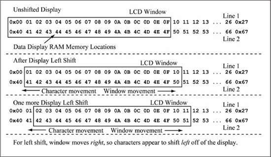
An internal address counter determines where the current data write operation places data. The address counter also specifies the cursor location. Initializing the display sets the address counter to zero, placing the cursor to the home position of location 0 (position 0 of line 1, upper-left corner of the display). A write data operation writes data to the current address location, then increments or decrements the address counter depending on the mode setting (entry mode set command in Table 8.4). In increment mode, the address counter is incremented by one and the cursor moves one position to the right on the display. Each additional write places data at the current address counter location, and increments the address counter. Assuming the display is unshifted, the 17th write (to location 16) places data “off-screen” (the data is not visible), but the data is still contained in DD RAM. A right shift of the display has to be performed to see the data contained in location 16. Each LCD command requires a fixed amount of time to execute. The PIC24 μC software communicating with the LCD can either have built-in delays that are guaranteed to exceed the required LCD command execution time, or the LCD can be polled via the read busy flag command to determine if the module is ready for another command. Before sending a command, a polling loop is used to continually read the busy flag status; the loop is exited when the busy flag returns 0. Other commands exist for loading custom character fonts; see the datasheet [34].
LCD Code Example
Listing 8.1 shows the macros used in the LCD C code to isolate the PIC24 μC port to LCD signal mapping. These correspond to the connections shown in Figure 8.28. Note that _LATBx assignments are used for outputs and _RBx are used for reading inputs.
Listing 8.1: LCD Interface Macros
#define RS_HIGH()         (_LATB9 = 1)
#define RS_LOW()          (_LATB9 = 0)
#define CONFIG_RS()       CONFIG_RB9_AS_DIG_OUTPUT()
#define RW_HIGH()         (_LATB13 = 1)
#define RW_LOW()          (_LATB13 = 0)
#define CONFIG_RW()       CONFIG_RB13_AS_DIG_OUTPUT()
#define E_HIGH()          (_LATB14 = 1)
#define E_LOW()           (_LATB14 = 0)
#define CONFIG_E()        CONFIG_RB14_AS_DIG_OUTPUT()

#define LCD4O             (_LATB5)
#define LCD5O             (_LATB6)
#define LCD6O             (_LATB7)
#define LCD7O             (_LATB8)
#define LCD7I             (_RB8)

#define CONFIG_LCD4_AS_INPUT()  CONFIG_RB5_AS_DIG_INPUT()
#define CONFIG_LCD5_AS_INPUT()  CONFIG_RB6_AS_DIG_INPUT()
#define CONFIG_LCD6_AS_INPUT()  CONFIG_RB7_AS_DIG_INPUT()
#define CONFIG_LCD7_AS_INPUT()  CONFIG_RB8_AS_DIG_INPUT()
#define CONFIG_LCD4_AS_OUTPUT() CONFIG_RB5_AS_DIG_OUTPUT()
#define CONFIG_LCD5_AS_OUTPUT() CONFIG_RB6_AS_DIG_OUTPUT()
#define CONFIG_LCD6_AS_OUTPUT() CONFIG_RB7_AS_DIG_OUTPUT()
#define CONFIG_LCD7_AS_OUTPUT() CONFIG_RB8_AS_DIG_OUTPUT()

#define GET_BUSY_FLAG()  (LCD7I)
Listing 8.2 shows some LCD utility functions. The configBusAsOutLCD() function is used to configure the pins used for the LCD D[7:4] as outputs for LCD write operations, while configBusAsInLCD() configures these same pins as inputs for LCD read operations. The outputToBusLCD(uint8_t u8_c) outputs the lower 4 bits of the u8_c argument to the LCD D[7:4] bus. The configControlLCD() function configures the ports used for the E, R/W# and RS signals and initializes them to a logic 0 value.
Listing 8.2: LCD Utility Functions
// Configure 4-bit data bus for output.
void configBusAsOutLCD(void) {
    RW_LOW();                     // RW=0 to stop LCD from driving pins
    CONFIG_LCD4_AS_OUTPUT();      // D4
    CONFIG_LCD5_AS_OUTPUT();      // D5
    CONFIG_LCD6_AS_OUTPUT();      // D6
    CONFIG_LCD7_AS_OUTPUT();      // D7
}

// Configure 4-bit data bus for input.
void configBusAsInLCD(void) {
    CONFIG_LCD4_AS_INPUT();       // D4
    CONFIG_LCD5_AS_INPUT();       // D5
    CONFIG_LCD6_AS_INPUT();       // D6
    CONFIG_LCD7_AS_INPUT();       // D7
    RW_HIGH();                    // R/W = 1, for read
}

// Output lower 4 bits of u8_c to LCD data lines.
void outputToBusLCD(uint8_t u8_c) {
    LCD4O = u8_c & 0x01;            // D4
    LCD5O = (u8_c >> 1) & 0x01;     // D5
    LCD6O = (u8_c >> 2) & 0x01;     // D6
    LCD7O = (u8_c >> 3) & 0x01;     // D7
}

// Configure the control lines for the LCD.
void configControlLCD(void) {
    CONFIG_RS();      // RS
    CONFIG_RW();      // RW
    CONFIG_E();       // E
    RW_LOW();
    E_LOW();
    RS_LOW();
}
Figure 8.30 shows two functions, pulseE() and writeLCD(), that are used for writing to the LCD using the macros and functions of Listings 8.1 and 8.2. The pulseE() function simply pulses the E signal line high with the DELAY_US(1) function calls providing more than enough delay for the pulse width and setup/hold times about the edges. The writeLCD() function writes one byte of data passed in u8_Cmd to the LCD, assuming a 4-bit interface. If u8_CheckBusy is non-zero, the busy flag is polled until it returns non-zero before performing the write. Observe that in the busy flag loop, the first read returns the upper 4 bits, while the second read returns the lower 4 bits. The busy flag is the MSb of the upper 4-bit transfer. Furthermore, the WDT is enabled during the busy flag polling loop so as to escape this infinite wait if there is a hardware failure (or to detect coding or wiring problems during testing). If u8_CheckBusy is zero, a pessimistic delay of 10 ms is performed before writing the byte instead of using the busy flag. After some commands, such as the function set command, the busy flag cannot be used so a delay must be performed instead. If u8_DataFlag is non-zero, the RS signal is set to 1 during the write; else it is set to 0. Finally, if u8_DataFlag is zero, only the upper 4 bits are written (the initial command that selects the 4-bit interface requires only a single 4-bit transfer as the LCD is in 8-bit mode on power-up).
The code in Figure 8.31 uses the writeLCD() function within the outStringLCD(char *psz_s) function to write the psz_s string to the LCD at the current cursor location. The main() code first calls configControlLCD() to configure the PIC24 μC port pins then calls initLCD(), which initializes the display using the commands of Table 8.4. Observe that none of the writeLCD() calls in initLCD() use the busy flag for status checking; instead, the constant delay mode of writeLCD() is used. After initialization, the address counter of the LCD is at location 0. The first outStringLCD() in main() writes to the first line of the LCD. Only the first 16 characters of the string passed to outStringLCD() are visible in the display, even though the entire string is stored in the LCD data display RAM. The following statement writeLCD(0xC0, 0, 1, 1) sets the internal address counter to 0x40 (first position of second line), so that the next outStringLCD() statement writes to the second line of the display. The 0xC0 byte in the writeLCD() function call is the Set DD address command, where 0xC0 = 0b1100000. The format of this command is 1nnnnnnn, where nnnnnnn is the data display address. Thus, the lower 7 bits of 0xC0 is 1000000, or 0x40, the address of the first location on the second line. An infinite loop is then entered in which the statement writeLCD(0x18, 0, 1, 1) is followed by a 0.3 second delay. The 0x18 (0x00011000) command byte is the Cursor & Display Shift command from Table 8.4 and has the format 0001cr00, with c = 1, r = 0 specifying a display left shift. The continual looping of this command causes the strings to scroll across the display moving right to left, with a 0.2 second delay between shifts. More sophisticated LCD modules allow graphical operations, such as turning on/off a pixel specified by an X, Y screen location.
Figure 8.30chap08lcd4bit.c. writeLCD(), pulseE() functions for the LCD interface
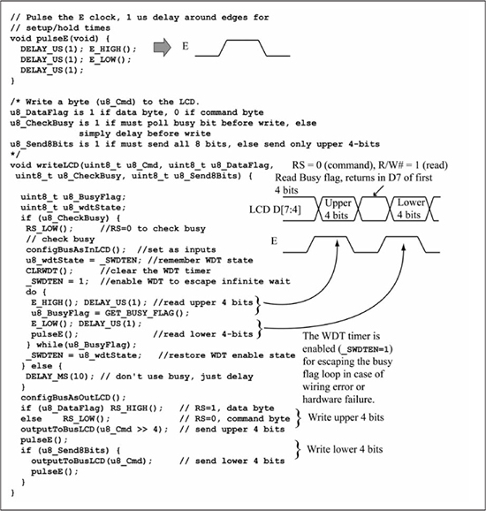
Figure 8.31chap08lcd4bit.c: Write two strings to LCD and shift display
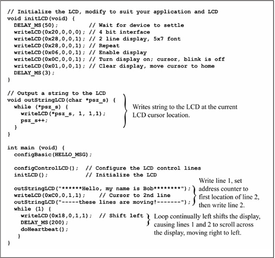
The PIC24E versus the PIC24F and PIC24H Families
The examples in this chapter have concentrated on the PIC24E family. Devices in the PIC24H and PIC24F families have the following principal differences (other differences exist):
![]() The PIC24F family has a maximum FCY of 16 MHz; the PIC24H has a maximum FCY of 40 MHz; the PIC24E supports an FCY of 60 MHz over its full temperature range, and 70 MHz for a limited temperature range.
The PIC24F family has a maximum FCY of 16 MHz; the PIC24H has a maximum FCY of 40 MHz; the PIC24E supports an FCY of 60 MHz over its full temperature range, and 70 MHz for a limited temperature range.
![]() The PIC24F family has a PLL with a fixed multiplication factor of 4X; the PIC24H and PIC24E offer a wide range of PLL multiplication factors.
The PIC24F family has a PLL with a fixed multiplication factor of 4X; the PIC24H and PIC24E offer a wide range of PLL multiplication factors.
![]() The PIC24F FRC oscillator has a nominal 8.0 MHz frequency versus 7.37 MHz for the PIC24H and PIC24E families. The 8.0 MHz FRC oscillator coupled with the 4X PLL offers a convenient method for achieving the maximum FCY of 16 MHz.
The PIC24F FRC oscillator has a nominal 8.0 MHz frequency versus 7.37 MHz for the PIC24H and PIC24E families. The 8.0 MHz FRC oscillator coupled with the 4X PLL offers a convenient method for achieving the maximum FCY of 16 MHz.
![]() The PIC24F family’s configuration bits are stored in two packed words instead of six for the PIC24H and PIC24E families. Approximately the same functionality is offered despite the difference in size.
The PIC24F family’s configuration bits are stored in two packed words instead of six for the PIC24H and PIC24E families. Approximately the same functionality is offered despite the difference in size.
![]() The PIC24E has added new capabilities to several of its peripheral modules (such as the input capture and output compare modules; see Chapter 12) but in all cases has maintained upward compatibility with the PIC24H in terms of module usage.
The PIC24E has added new capabilities to several of its peripheral modules (such as the input capture and output compare modules; see Chapter 12) but in all cases has maintained upward compatibility with the PIC24H in terms of module usage.
This book’s examples are compatible with the PIC24E/H/F and dsPIC33E/F families. Built-in compiler macros such as __PIC24E__ and __PIC24H__ have been used to differentiate code between families when needed. While all of the book’s examples have been tested with the dsPIC33EP128GP502 and the PIC24HJ32GP202, many of them have also been tested with the PIC24FJ64GA002, which is a 28-pin PIC24F μC that is pin compatible with the dsPIC33EP128GP502.
Summary
Code written in a high-level language (HLL) such as C is usually clearer in its intent, has fewer source lines, and is more portable than code written in assembly language. As such, many microcontroller applications are written in an HLL rather than assembly. However, understanding assembly language and the implementation of HLL constructs in assembly language is critical in writing efficient HLL microcontroller applications. The MPLAB® PIC24 compiler is used for the examples in this book and provides a powerful tool for experimenting with PIC24 applications. A simple PIC24 hardware system with a power source, a reset switch, and serial interface is used to demonstrate the basics of parallel port I/O, reset sources, and power saving modes. A PIC24 μC has many different sources of reset, with status bits in the RCON register used to determine the reset source. Reducing power consumption is an issue in many microcontroller applications, and the sleep, idle, and doze modes in the PIC24 μC can be used to reduce current draw. The watchdog timer runs on an independent clock source, and can be used to wake the PIC24 from sleep and idle modes to resume execution. The PIC24 has multiple parallel port I/O pins with bidirectional transfer capability as well as open-drain and weak pull-up functionality. An LCD module interface in 4-bit mode can be implemented using eight of the parallel port pins on the PIC24.
Review Problems
Assume that the target device is the dsPIC33EP128GP502 μC for all problems.
1. Give the special function register bit settings that configure RB5 as a digital input, with weak pull-up disabled, and open-drain disabled.
2. Give the special function register bit settings that configure RB6 as a digital output, with weak pull-up disabled, and open-drain enabled.
3. Give the special function register bit settings that configure RB2 as a digital input, with weak pull-up enabled, and open-drain disabled.
4. Give the special function register bit settings that configure RB3 as a digital output, with weak pull-up disabled, and open-drain disabled.
5. Repeat problem 1, but use the macros discussed in this chapter to configure the given pin.
6. Repeat problem 2, but use the macros discussed in this chapter to configure the given pin.
7. Using the data of Table 8.2 for the dsPIC33EP128GP502, predict the doze mode current for FCY/4.
8. Using the data of Table 8.2 for the dsPIC33EP128GP502, predict the doze mode current for FCY/8.
9. For the following code segment, predict what you will see occur once power is applied, and explain your reasoning.
int main() {
  ...normal config, including uart...
  outString(“Howdy Y’all!
”);
  _SWDTEN = 1;
  while(1);
}
10. For the following code segment, predict what you will see occur once power is applied, and explain your reasoning.
int main() {
  ...normal config, including uart...
  outString(“Howdy Y’all!
”);
  if (_POR) {
    _SWDTEN = 1;
    _POR = 0;
  } else {
    _SWDTEN = 0;
  }
  while(1);
}
11. For the following code segment, predict what you will see occur once power is applied, and explain your reasoning.
int main() {
  ...normal config, including uart...
  outString(“Howdy Y’all!
”);
  asm(“pwrsav #0”);
  while(1);
}
12. For the following code segment, predict what you will see occur once power is applied, and explain your reasoning.
int main() {
  ...normal config, including uart...
  outString(“Howdy Y’all!
”);
  _SWDTEN = 1;
  asm(“pwrsav #0”);
  while(1);
}
The following problems assume external LEDs (LED1, LED2, and so on) and switches (SW1, SW2, and so on). When writing code for these problems, define macros for them as done in Figure 8.22 using the predefined macros in libincludepic24_ports.h. You may use any of the RBn ports you want to implement these problems. Assume switch inputs are pushbutton inputs, and use the internal weak pull-up of the port.
13. Assume one LED (LED1) and one switch input (SW1). Write a while (1) loop that initially will blink an LED1 once power is applied. On each press AND release of SW1, alternate between terminating the blinking and resuming the blinking. Draw a state machine chart for the problem, and implement it using the style of Figure 8.24.
14. Assume two LEDs (LED1, LED2) and one switch input (SW1). Both LEDs should be initially off. After each press AND release of SW1, change the LED state (LED1/LED2) in the sequence: OFF/ON, ON/OFF, ON/ON, OFF/OFF, OFF/ON, ON/OFF, ON/ON, OFF/OFF, and so on. Draw a state machine chart for the problem, and implement it using the style of Figure 8.24.
15. Do problem #14, except the LEDs change state whenever a press OR a release occurs for SW1.
16. Do problem #13, except the blinking terminates or resumes whenever a press OR a release occurs for SW1.
For Figure 8.32, assume that macros named DFF_D, DFF_CK, DFF_R, DFF_S, and DFF_Q have been defined for the RB? pins connected to the external D flip-flop (refer to Chapter 1 for a review of D flip-flop operation).
Figure 8.32
PIC24 μC to D flip-flop
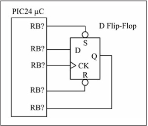
17. Write a C function named uint8_t testDFFASync(uint8_t u8_op) that asynchronously resets the DFF if u8_op is non-zero, else an asynchronous set is performed. The function should return a true (non-zero uint8_t value) if the Q output returns the correct output value, else return a false value (zero). Assume nothing about the initial output states of the RB? ports when entering the function (you may assume that they have already been configured to be inputs or outputs as appropriate). When exiting the function, all outputs should be at their negated values (D, CK at 0; S, R at 1). For emphasis purposes only, use a 1 μs software delay to satisfy pulse width times, setup/hold times for the D input with regard to the clock, and propagation delay through the DFF once the inputs have been applied.
18. Write a C function named uint8_t testDFFSync(uint8_t u8_dval) that synchronously clocks in a 1 to the DFF from the D input if u8_dval is non-zero, and a 0 otherwise. The function should return a true (non-zero uint8_t value) if the Q output returns the correct output value, else return a false value (zero). Assume nothing about the initial output states of the RB? ports when entering the function (you may assume that they have already been configured to be inputs or outputs as appropriate). When exiting the function, all outputs should be at their negated values (D, CK at 0; S, R at 1). For emphasis purposes only, use a 1 μs software delay to satisfy pulse width times, setup/hold times for the D input with regard to the clock, and propagation delay through the DFF once the inputs have been applied.
For Figure 8.33, assume that macros named GATE_A, GATE_B, and GATE_Y have been defined for the RB? pins connected to the external NAND gate (refer to Chapter 1 for a review of the NAND operation).
Figure 8.33
PIC24 μC to NAND gate
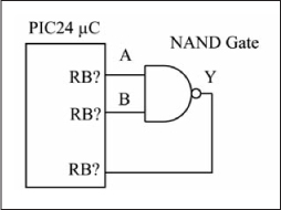
19. Write a C function named uint8_t testGate(void) that exhaustively applies all input combinations to the external gate. If the gate output returns the wrong output value for an input combination, terminate the test and return a false (zero) value. If the gate returns the correct output value for all input combinations, then return a true (non-zero uint8_t value). Assume nothing about the initial output states of the RB? ports when entering the function (you may assume that they have already been configured to be inputs or outputs as appropriate). For emphasis purposes only, use a 1 μs software delay before reading the Y output after applying an input combination.
20. Repeat problem #19 except use an XOR gate as the external gate.