CHAPTER 2
THE STORED PROGRAM MACHINE
This chapter introduces the fundamental concepts of computer operation by implementing a controller both as a finite state machine and as a stored program machine.
Learning Objectives
After reading this chapter, you will be able to:
![]() Compare and contrast controller designs using finite state machine and stored program machine approaches.
Compare and contrast controller designs using finite state machine and stored program machine approaches.
![]() Describe the operation of a finite state machine via an algorithmic state machine chart.
Describe the operation of a finite state machine via an algorithmic state machine chart.
![]() Implement a finite state machine using a one-hot state encoding method.
Implement a finite state machine using a one-hot state encoding method.
![]() Discuss the basic elements of a stored program machine.
Discuss the basic elements of a stored program machine.
![]() Describe the meaning of the terms opcode, machine word, instruction mnemonic, address bus, data bus, instruction pointer, assembly, and disassembly.
Describe the meaning of the terms opcode, machine word, instruction mnemonic, address bus, data bus, instruction pointer, assembly, and disassembly.
![]() Describe the fetch and execute sequence of a stored program machine.
Describe the fetch and execute sequence of a stored program machine.
![]() Convert a simple assembly language program to machine code and vice versa.
Convert a simple assembly language program to machine code and vice versa.
![]() Follow the execution of a simple assembly language program.
Follow the execution of a simple assembly language program.
![]() Write a simple assembly language program to solve a specified problem.
Write a simple assembly language program to solve a specified problem.
The preceding tasks introduce you to the concept of stored program machines, of which the PIC24 family of microcontrollers is a prime example, and is the principal focus of the rest of this book. The PIC24 family of microcontrollers is simply a more complex version of the stored program machine discussed in the following sections. This chapter provides you with the first chance to dip your toes into the vast ocean of microprocessor operation, programming, and application.
Problem Solving the Digital Way
Digital systems provide solutions for problems in which real-world inputs can be converted to a digital representation, which is then processed by a clever use of combinational and sequential building blocks to produce a digital output that is converted back to a useful quantity in the real world. As an example, consider a digital voice recorder:
![]() Pushbutton inputs on the recorder determine if the recorder is in record mode or playback mode. A microphone input with a biasing circuit converts voice that varies in amplitude over time to a continuously varying voltage, where the voltage fluctuations are the sound wave variations of human speech.
Pushbutton inputs on the recorder determine if the recorder is in record mode or playback mode. A microphone input with a biasing circuit converts voice that varies in amplitude over time to a continuously varying voltage, where the voltage fluctuations are the sound wave variations of human speech.
![]() A building block called an analog-to-digital converter (ADC) produces a digital (binary) representation of the microphone output voltage at regular time intervals. Each converted digital value is called a voice sample.
A building block called an analog-to-digital converter (ADC) produces a digital (binary) representation of the microphone output voltage at regular time intervals. Each converted digital value is called a voice sample.
![]() A digital building block called a controller monitors the button inputs on the recorder.
A digital building block called a controller monitors the button inputs on the recorder.
![]() In record mode, the controller reads the voice samples from the ADC and stores them in a memory device.
In record mode, the controller reads the voice samples from the ADC and stores them in a memory device.
![]() In playback mode, the controller reads the memory contents sequentially and sends each voice sample to a building block called a digital-to-analog converter (DAC) that converts a digital input value to a voltage. This voltage signal drives a speaker, allowing the recorded voice to be heard.
In playback mode, the controller reads the memory contents sequentially and sends each voice sample to a building block called a digital-to-analog converter (DAC) that converts a digital input value to a voltage. This voltage signal drives a speaker, allowing the recorded voice to be heard.
Analog-to-digital converters and digital-to-analog converters are essential parts of digital systems and are covered in Chapter 11. This chapter is concerned with the design of the controller that sequences events within a digital system.
Two basic choices exist for building a controller: a finite state machine (FSM) or a stored program machine (also known as a Von Neumann machine after the scientist who first proposed this approach [1], [2]). In an FSM, dedicated logic implements the event sequence required for a task. In a stored program machine, data stored in a memory specifies the event sequence for a particular task. An advantage of an FSM is that it usually takes fewer clock cycles than a stored program machine to perform a particular task. The principal advantage of a stored program machine is flexibility; a different task can be implemented by simply changing memory contents. An FSM requires redesign of its internal logic to implement a different task, which is a much more difficult problem than memory modification.
To illustrate the differences between these approaches, consider a digital system that continuously outputs the digits of a phone number, Y1Y2Y3-Z1Z2Z3Z4. In local mode, only digits Z1Z2Z3Z4 are output, while in non-local mode all digits are output. In the controller designs for this problem, a common set of inputs and outputs is used for comparison purposes:
![]() LOC (input): When 1, the system is in local mode; when 0, in non-local mode.
LOC (input): When 1, the system is in local mode; when 0, in non-local mode.
![]() CLK (input): This is obviously a sequential system, as the output cannot be solely determined by the LOC input, so the system requires DFFs, which implies that a clock input is needed.
CLK (input): This is obviously a sequential system, as the output cannot be solely determined by the LOC input, so the system requires DFFs, which implies that a clock input is needed.
![]() RESET# (input): All sequential digital systems need an input signal that initializes the internal DFFs to a known state after power is applied, because the internal state of DFFs are indeterminate on power-up. This signal is usually called RESET#; the # in the name indicates that this input is low-true.
RESET# (input): All sequential digital systems need an input signal that initializes the internal DFFs to a known state after power is applied, because the internal state of DFFs are indeterminate on power-up. This signal is usually called RESET#; the # in the name indicates that this input is low-true.
![]() DOUT[3:0] (output): This 4-bit output bus is used to sequentially output the digits of the phone number. A digit has a value between 0 and 9, so 4 bits are sufficient for encoding purposes. Binary encoding is used for these digits.
DOUT[3:0] (output): This 4-bit output bus is used to sequentially output the digits of the phone number. A digit has a value between 0 and 9, so 4 bits are sufficient for encoding purposes. Binary encoding is used for these digits.
The following sections detail controller designs using both FSM and stored program machine approaches. Contrasting the two controller designs emphasizes the strengths and weaknesses of each approach.
Finite State Machine Design
An FSM can be thought of as a sequential building block that is custom-designed to solve a particular problem. The problem solved by an FSM is described as a series of transitions between states, where a transition from the present state to the next state is determined by the present state and the current inputs. A state can be thought of as one of the steps within a sequence of steps that are required to accomplish some task. The steps that come before and after it uniquely identify a state. The outputs of the FSM are also determined either by only the present state or a combination of the present state and current inputs. In this example, you use an algorithmic state machine (ASM) chart to describe the state sequencing of an FSM. An ASM chart is similar to a software flowchart for those familiar with that notation. Symbols used in an ASM chart are:
![]() Rectangle: This indicates a state. Outputs asserted during this state are written within the rectangle; these outputs are called unconditional outputs, as the assertion is dependent only upon the state, not upon any external input. Any outputs that do not appear in a state are assumed negated.
Rectangle: This indicates a state. Outputs asserted during this state are written within the rectangle; these outputs are called unconditional outputs, as the assertion is dependent only upon the state, not upon any external input. Any outputs that do not appear in a state are assumed negated.
![]() Diamond: This is a decision point. The diamond contains the input that the decision is based upon.
Diamond: This is a decision point. The diamond contains the input that the decision is based upon.
![]() Oval: This can only appear after a decision point and is used for conditional outputs, which is an output dependent upon both a state and some set of inputs.
Oval: This can only appear after a decision point and is used for conditional outputs, which is an output dependent upon both a state and some set of inputs.
![]() Circle: This appears next to each state and contains the state name.
Circle: This appears next to each state and contains the state name.
The ASM chart in Figure 2.1 shows an FSM that outputs the number 324-8561 according to the problem specification. The ASM contains seven states with the S* state being the state entered upon reset (the reset state is designated by the * symbol). The state following S* is dependent upon the LOC input; if LOC = 1, then the next state is Z2, otherwise the next state is Y2. The state progression for LOC = 0 is S*, Y2, Y3, Z1, Z2, Z3, Z4, which then loops back to S*. Each state requires one clock cycle, so this state progression requires seven clock cycles. If LOC = 1, the state progression is S*, Z2, Z3, Z4, again looping back to state S*. The LOC input is only checked in the S* state, so the sequence cannot be altered once state S* has been exited. The DOUT output of the S* state is conditional upon the LOC input; DOUT = 8 if LOC = 1, otherwise DOUT = 3. The DOUT output in all other states is unconditional.
Figure 2.1
ASM chart for the number sequence 324-8561

Finite State Machine Implementation
A generic block diagram of an FSM implementation is shown in Figure 2.2. The state DFFs contain the present state of the FSM. The CLOGIC block is the combinational logic that produces the next state inputs to the state DFFs based on the present state and external inputs. State changes occur on the active clock edge.
Figure 2.2
Finite state machine block diagram
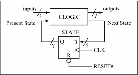
The first task in implementing this FSM is state assignment, which means assigning binary encodings for each state. The state assignment affects the number of state DFFs required and the combinational logic within the CLOGIC block. Table 2.1 lists two choices for state encoding; there are many others. Using binary encoding requires only three DFFs but more complex combinational logic; one-hot encoding requires one DFF per state (for a total of seven), but simplifies the task of determining the required combinational logic equations. This is meant as an illustrative exercise, and not an exhaustive treatise on FSM design, so it uses one-hot encoding.
Table 2.1: Two Possibilities for State Assignment

Two sets of Boolean equations are required for the CLOGIC block: the set that controls the state sequencing and the set that produces the required output values. The set of Boolean equations that controls the state sequencing consists of seven equations, one for each D input of a DFF. An advantage of one-hot encoding is that these equations can be easily determined by inspection of the ASM chart. As an example, consider the equation for the D input of state S*, designated by D_S*. This state is entered on the next clock cycle from state Z4, and you know that the Q output of the state Z4 DFF, denoted by Q_Z4, will only be a 1 when the FSM is in state Z4. Thus, the D_S* Boolean equation has only one term, as shown in Equation 2.1.
The equation for the D input of the Y2 state is a bit more interesting, as this state is entered only if the current state is S* and LOC is 0, as stated in Equation 2.2.
The Boolean equations for the remaining DFF inputs are derived through similar reasoning, as shown in Equations 2.3 through 2.7.

The previous Boolean equations for state sequencing do not include the reset behavior. The reset signal input is tied to the set (S) input of the DFF for state S* and to the reset (R) input of the remaining state DFFs. In this way, reset assertion forces the FSM to enter state S* while reset negation allows normal state sequencing.
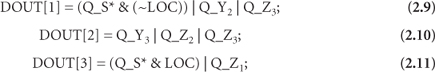
The Boolean equations for the DOUT outputs depend upon the current state and LOC input values. Table 2.2 lists the binary output values for DOUT given the current state and LOC values.
A Boolean logic equation is needed for each of the 4 bits of DOUT. We will write these equations by inspection and make no attempt at minimizing the amount of logic required for implementation. From Table 2.2, you can see that the DOUT[0] output is a 1 for the following conditions: in state S* and LOC = 0, or in states Z2 or Z4. This is expressed as a Boolean equation for the DOUT[0] output as shown in Equation 2.8.
Table 2.2: Output Values for DOUT Referenced to States

The equations for the other DOUT bits are derived similarly, as shown in Equations 2.9 through 2.11.
These Boolean equations can be mapped to logic gates for implementation; a simulation of the resulting gate level system is shown in Figure 2.3. Note that in clock cycle #1, the system is in state S* with DOUT = 3, but when state S* is reentered in clock cycle #8 the output is DOUT = 8, because now LOC = 1 (the changing of the LOC input value is arbitrary as it is an external input; it is changed in clock cycle #5 to illustrate that the LOC input affects only the FSM behavior in state S*).
Figure 2.3
Simulation of the FSM implementation

Note that if the phone number is changed, only the Boolean equations for DOUT must be changed; the Boolean equations for the state sequencing remain the same. However, if the number of phone digits is changed, say to X1X2X3-Y1Y2Y3-Z1Z2Z3Z4, this requires a new state sequence and hence different logic for state sequencing. This highlights the disadvantage of the FSM approach; changes to the circuit functionality require a logic redesign.
A Stored Program Machine
A stored program machine is the formal term for a computer. Three components of every stored program machine are:
![]() Input/Output (I/O) signals that are used for interfacing with the external world.
Input/Output (I/O) signals that are used for interfacing with the external world.
![]() Memory that stores the instructions that determine the sequence of events performed by the computer. An instruction is a binary datum that is usually a fixed width. Memory also stores data that instructions manipulate.
Memory that stores the instructions that determine the sequence of events performed by the computer. An instruction is a binary datum that is usually a fixed width. Memory also stores data that instructions manipulate.
![]() Control logic that decodes the instructions and executes the actions specified by an instruction.
Control logic that decodes the instructions and executes the actions specified by an instruction.
The common elements between a finite state machine and a stored program machine are I/O and control; the memory component is the differentiating factor. Memory provides flexibility for a stored program machine; a stored program machine can be programmed to perform a different task by changing the instructions stored in memory. A program is a sequence of instructions that implement a particular task. A stored program machine continuously performs a fetch/execute action, in which an instruction is fetched from memory then executed. Instruction fetches typically progress through memory in a sequential manner. Instructions are divided into different classes; some instructions perform arithmetic operations, some perform input/output, and some perform control. An example of arithmetic instruction execution is binary addition. An example of an input/output instruction execution is placing a data value on an output bus. An example of a control instruction execution is a goto X (jump) that fetches the next instruction from location X instead of the next sequential memory location.
Instruction Set Design and Assembly Language
The design of the stored program machine begins with determining what type of instructions it should execute and the format or binary encoding of these instructions. To determine this, we will describe the task as a sequence of statements in the C programming language, as seen in Listing 2.1.
Listing 2.1 C Language Program of the Number Sequencing Task
START:
 if (loc) goto LOCAL;
 dout = 3;
 dout = 2;
 dout = 4;
LOCAL:
 dout = 8;
 dout = 5;
 dout = 6;
 dout = 1;
 goto START;
These statements represent three distinct operations:
![]() An output operation as specified by the statement
An output operation as specified by the statement dout = 2, which places the value 0b0010 on the DOUT data bus.
![]() An unconditional transfer of control, also known as a goto or jump, as specified by the statement
An unconditional transfer of control, also known as a goto or jump, as specified by the statement goto START, which says to fetch the next instruction from the memory location represented by the label START.
![]() A conditional transfer of control, also known as a branch or a conditional jump, as specified by the statement
A conditional transfer of control, also known as a branch or a conditional jump, as specified by the statement if (loc) goto LOCAL. If loc is non-zero (i.e., true), the next instruction fetched is the one at label LOCAL. If loc is zero (i.e., false), the next sequential instruction in memory is fetched, which in this case is dout = 3.
These instruction types must be assigned a binary encoding so that they can be stored in memory. The encoding of an instruction must specify the type of instruction and the data required by the instruction (if the instruction requires data). The instruction bits that specify the instruction type form a bit field that is called the opcode. The data required by the instruction is more formally known as the operand. Figure 2.4 illustrates how instruction encoding is divided into opcode and operand fields.
Figure 2.4
Instruction encoding split into opcode and operand fields

Two bits are needed for the opcode to encode the three types of instructions in the computer. Table 2.3 lists the instruction set for the number sequencing computer (NSC). The leftmost column contains the instruction mnemonic, which is the human-readable form of an instruction. The middle column gives the opcode encoding and the rightmost column the instruction operand.
Table 2.3: Instruction Encodings for the Number Sequencing Computer

Opcode encoding is usually chosen so that classes of instructions can be easily distinguished. In this case, the two control instructions JC and JMP are distinguished from the I/O instruction OUT by the most significant bit of the opcode. The OUT instruction operand is the 4-bit digit that appears on the DOUT data bus after the instruction is executed. The JMP and JC instructions have the same type of operand, which is the memory address of the target instruction of the jump. The number of bits required for this memory address depends on the maximum number of memory locations allowed in our number sequencing computer. For now, a total of 4 bits is used, which limits the total number of memory locations to 24 = 16. Each memory location contains one instruction, so the maximum number of instructions in any program written for the computer is 16 instructions. Each of the instructions is 6 bits wide (2 bits of opcode, 4 bits of data), so a 16x6 memory device is required for storing the instructions of the program.
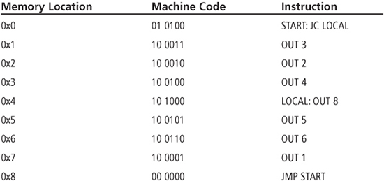
Listing 2.2 gives the C program of the number sequencing task translated into the instructions used by our computer. The translation of a high-level language to the native instructions of a computer is called compilation. A program specified using the instruction mnemonics of an instruction set is called an assembly language program. A computer program called a compiler is normally used to translate a high-level language program to assembly language, but in this book the process is done manually in many cases to illustrate the linkage between C statements and assembly language statements. The lines START : and LOCAL: are called labels and are not instructions. They are used as identifiers for particular program lines, and the reasoning for including them will soon become clear.
Listing 2.2 Assembly Language Program for the Number Sequencing Task
START:
 JC LOCAL
 OUT 3
 OUT 2
 OUT 4
LOCAL:
 OUT 8
 OUT 5
 OUT 6
 OUT 1
 JMP START
The next step is to translate the program into binary so that it can be stored in memory. This process is called assembly and is performed by a computer program called an assembler. The resulting binary codes are called the machine code of the assembly language program. The reverse process of converting machine code to assembly language mnemonics is called disassembly. The assembly process is done in two passes by the assembler; the first pass assembly does not assemble any JMP/JC instructions whose jump destination is ahead of the current instruction as the memory location of the jump destination is unknown. After the first pass assembly, the locations of all instructions are known so the second pass completes the assembly of any JMP/JC instructions that were not completed in the first pass. Table 2.4 gives the first pass result of this assembly process. The leftmost column contains the memory location where the machine code for the instruction is placed. You’ll place the instructions starting at location 0x0 in memory for reasons that are explained later. Each assembly language statement is translated individually to its machine code representation. Observe that the operand field of the first instruction is left as “????” because the location of the instruction represented by the label LOCAL is unknown by the assembler when this instruction is assembled during the first pass. The last instruction, JMP START, can be completely translated by the assembler because the label START stands for the first instruction, which has already been translated and is located at location 0x0.
Table 2.4: First Pass Assembly of the Number Sequencing Program

Once the first pass assembly is complete, you see that the value for label LOCAL is the memory address 0x4. Table 2.5 gives the second pass assembly of the number sequencing program; the values of all labels are now known so the machine code translation is complete.
Table 2.5: Second Pass Assembly of the Number Sequencing Program
The program consists of nine assembly language instructions; the remaining seven locations of the 16x6 memory are not needed for this program.
Hardware Design
You must now design hardware that executes the machine code program of the number sequencing task. You will use the sequential blocks covered in the first chapter to make the job easier. Figure 2.5 shows what is currently known about the hardware components of our computer; it has a 16x6 memory, a 1-bit input called LOC, and a 4-bit output called DOUT.
Figure 2.5
Number sequencing computer initial components

In looking at Figure 2.5, you can see several busses (DOUT, the memory address bus, and the memory data bus) that connect to nothing, so this provides a logical place to begin adding components. Recall that a register is a sequential building block used to hold a value over one or more clock cycles. A 4-bit register is needed to drive the DOUT data bus; the register contents are modified by execution of the OUT instruction. Recall that a counter is a register that has the capability of counting up or down, or both. Instructions are usually fetched sequentially from memory, which means that the addresses provided to memory generally proceed in binary counting order. Thus, a 4-bit counter is the natural choice for providing the address to memory. This counter is an integral part of any computer and is known as the program counter (PC) or instruction pointer (IP). The PC register contains the address of the instruction currently being fetched from memory. Figure 2.6 shows the number sequencing computer hardware modified to contain the PC and output registers and supplemented with logic that controls these registers’ operation.
Figure 2.6
Number sequencing computer with program counter, output register, and control logic

The reset inputs of the PC and output register are tied to the external reset input. When reset is asserted, the PC register is cleared, which means the first instruction fetched from memory is at location 0, requiring the instructions in Table 2.5 to begin at location 0. Observe that the LD and INC control inputs of the PC and the LD input of the output register now connect to a general block named control. Modification of the PC and output registers is controlled by the current instruction. Table 2.6 lists the PC and output register control input values for each instruction.
The output register is loaded when the OUT instruction is executed. The PC register is incremented if an OUT instruction is executed or when a JC instruction is executed and LOC = 0. The PC register is loaded when a JMP instruction is executed or when a JC instruction is executed and LOC = 1.
Table 2.6: PC, Output Register Inputs for Instruction Execution
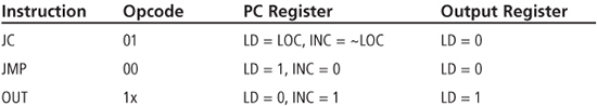
The Boolean equations for the PC and output register control lines are shown in Equations 2.12 through 2.14 as determined from Table 2.6. To simplify the resulting equations, an opcode of 1x instead of 11 was used for the OUT instruction.
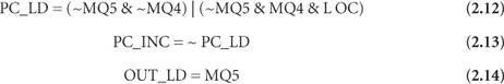
The values MQ5 and MQ4 are the two most significant bits of the instruction word fetched from memory; these are the opcode bits of the instruction. The Boolean equation for the PC_INC signal is simply the complement of PC_LD, as the PC is incremented if it is not being loaded. The logic gates that implement the Boolean equations for PC_LD, PC_INC, and OUT_LD are placed in the control logic block, as shown in Figure 2.7, which completes the design.
Figure 2.8 shows a simulation of the number sequencing computer. The PC waveform is the program counter value and is useful for tracking the instruction execution progress.
Table 2.7 compares the number of clock cycles required for each number sequence in the finite state machine and stored program machine implementations. The stored program machine requires two more clock cycles for each sequence because of the JC instruction at the beginning of the sequence and the JMP at the end of the sequence. In general, a stored program machine will take more clock cycles to accomplish a task than a finite state machine, which is the penalty for increased flexibility and is a typical trade-off when evaluating whether to use a general-purpose computer versus dedicated logic as a problem solution.
Figure 2.7
Complete hardware design for the number sequencing computer

Figure 2.8
Simulation of the number sequencing computer
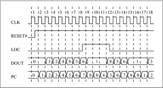
Table 2.7: FSM versus SPM Clock Cycles

Modern Computers
How does the number sequencing computer (NSC) compare against modern computers?
![]() Programs for the NSC reside in memory that has a maximum of 16 locations; modern computers have memory that contains billions of locations.
Programs for the NSC reside in memory that has a maximum of 16 locations; modern computers have memory that contains billions of locations.
![]() The data register in the NSC is 4 bits wide; modern computers have data registers that are typically 32 or 64 bits wide, and even larger in some cases.
The data register in the NSC is 4 bits wide; modern computers have data registers that are typically 32 or 64 bits wide, and even larger in some cases.
![]() The NSC has three different instructions; modern computers have tens to hundreds of different instructions.
The NSC has three different instructions; modern computers have tens to hundreds of different instructions.
![]() The NSC can be implemented in less than 100 logic gates; modern computers can require millions of logic gates.
The NSC can be implemented in less than 100 logic gates; modern computers can require millions of logic gates.
Despite these differences, the NSC and modern computers share the basic components of all computers: input/output, memory, and control. These three components work together to fetch and execute instructions that are stored in memory.
Summary
This chapter introduced the basic concepts of stored program machines. Stored program machines offer more flexibility than finite state machines at the cost of lower performance. The next chapter introduces the stored program machine that is the main topic of this book, the PIC24 microcontroller.
Review Problems
The answers to the odd-numbered problems can be found in Appendix C.
1. Write an assembly language program for the number sequencing computer that outputs the four digit sequence 0, 2, 5, 7 if LOC = 0, otherwise output the sequence 1, 3, 6, 8. After a sequence is finished, loop back to program start. Convert your assembly language program to machine code starting at location 0.
2. Write the assembly language program corresponding to the NSC machine code program seen in Table 2.8.
3. For the NSC, assume that the LOC input is tied to the least significant bit of the DOUT bus. For the program in Table 2.9, give the location executed and the DOUT value for the first 10 clock cycles.
Table 2.8: NSC Machine Code Program

Table 2.9: NSC Assembly Language Program

4. Repeat problem #3, except change the instruction at location #1 to OUT 4.
5. Assume the number definition is changed to 1-X1X2X3-Y1Y2Y3-Z1Z2Z3Z4, with the local number as Y1Y2Y3-Z1Z2Z3Z4. How many instructions are required for the NSC to implement this program?
6. Modify the schematic of the NSC (Figure 2.7) to add support for a new instruction called INC that increments the current contents of the output register. Assign this new instruction the binary opcode 11; the data field is unused. (Hint: Try replacing the output register with an up counter.)
7. Modify the schematic of the NSC (Figure 2.7) so that it can access a memory with 32 instructions. (Hint: Begin by extending the memory to 32 locations, then trace all of the changes required in the various components—you may be surprised at the number of modifications caused by this seemingly minor extension.)
8. Assume the NSC has a new instruction called INC (opcode = 11) that increments the contents of the OUT register; the INC instruction data field is unused. Also assume that the LOC input is tied to the complement of the DOUT[3] bit (LOC = ~DOUT3). For the program in Table 2.10, how many clock cycles does it take to reach location 3?
Table 2.10: NSC Assembly Language Program

9. What changes have to be made to the NSC (Figure 2.7) to accommodate a maximum of eight instructions instead of four?
10. Assume the number definition is changed to 1-X1X2X3-Y1Y2Y3-Z1Z2Z3Z4, with the local number as Y1Y2Y3-Z1Z2Z3Z4. Draw the new ASM chart required to implement this number sequence. How many states are required? If binary encoding is used for the states, how many DFFs are required?