
CHAPTER 12
TIMERS
Use of timers for periodic interrupt generation was previously discussed in Chapter 9. However, that discussion only scratched the surface of the capabilities and application of the PIC24 timer subsystems. This chapter discusses the use of PIC24 timers for time measurement, waveform generation, real-time clock keeping, and pulse width modulation. Example applications include biphase waveform decoding for infrared reception, servo positioning, and DC motor speed control.
Learning Objectives
After reading this chapter, you will be able to:
![]() Discuss the specifics of the Timer1, Timer2, and Timer3 subsystems.
Discuss the specifics of the Timer1, Timer2, and Timer3 subsystems.
![]() Use the input capture subsystem to perform precise time measurements of external events.
Use the input capture subsystem to perform precise time measurements of external events.
![]() Use the input capture subsystem to decode an infrared receiver’s output signal that is either space-width encoded or biphase encoded.
Use the input capture subsystem to decode an infrared receiver’s output signal that is either space-width encoded or biphase encoded.
![]() Use the pulse width modulation capability of the output compare module to generate square waves with varying duty cycles and periods, which can be used to control the brightness of an external LED, servo position, and DC motor speed.
Use the pulse width modulation capability of the output compare module to generate square waves with varying duty cycles and periods, which can be used to control the brightness of an external LED, servo position, and DC motor speed.
![]() Implement a simple real-time clock using a 32.768 kHz clock source and Timer1.
Implement a simple real-time clock using a 32.768 kHz clock source and Timer1.
![]() Use the real-time clock calendar (RTCC) module and a 32.768 kHz clock source for time/date tracking.
Use the real-time clock calendar (RTCC) module and a 32.768 kHz clock source for time/date tracking.
Pulse Width Measurement
The word timer implies time measurement, and a fundamental timer application is time measurement between two external events. In the digital world, an external event is either a rising or falling edge on an input pin. The time between two edges of the same type (falling-to-falling edge or rising-to-rising edge) on a square wave is the period, while the time between a rising-to-falling edge and falling-to-rising edge is high pulse width and low pulse width, respectively. The basics of event measurement are explored using the setup of Figure 12.1, in which the goal is to measure the low pulse width produced by activating a momentary switch. As a word of caution, if precise time measurement is required then you cannot use the internal fast RC oscillator since its period varies significantly (± 2%) from processor to processor and with temperature and VDD. As such, use of an external crystal oscillator or other stable external clock source is needed if precision time measurements are desired. Examples in this chapter typically use an external 8 MHz crystal for accuracy purposes and are configured for operation with the internal PLL to generate a 40 MHz FCY for compatibility with both the PIC24H/dsPIC33F and PIC24E/dsPIC33E families, instead of the 60 MHz FCY used with the reference system of Chapter 8.
Figure 12.1
Pulse width measurement

A straightforward method of measuring the pulse width of Figure 12.1 is given by the code of Figure 12.2, which uses Timer2 and polling of the switch input. Timer2 is configured for the maximum period (PR2 = 0xFFFF), with a prescaler of 256, which gives a period of approximately 420 ms (one timer tick ~ 6.4 μs) at FCY = 40 MHz; see Figure 9.11 for a review of Timer2 configuration. The while (1) loop waits for a low input value (falling edge) on the pushbutton input then stores the TMR2 value in u16_start. The code then waits for a high input value (rising edge) and computes the difference between the two TMR2 tick values as:
u16_delta = TMR2 - u16_start;
This 16-bit delta calculation is correct only if the pulse width does not exceed the timer’s maximum period. The u16_delta value represents the difference between the two TMR2 values even if the timer rolls over (overflows) between reading of the two values because the PR2 value is at its maximum value of 0xFFFF. If Timer2 is not configured for a maximum period, then the code would have to be replaced with:
u16_end = TMR2;
   if (u16_end > u16_start) u16_delta = u16_end - u16_start;
   else u16_delta = PR2+1 - u16_start + u16_end;
The else clause is the case for the u16_end value being read after the timer rolls over from its maximum value of PR2 to 0x0000. Observe that if PR2 = 0xFFFF, then PR2+1 is equal to 0x0000, so the else clause devolves to u16_end - u16_start. If the pulse width is longer than a timer period, then the number of timer rollovers must be tracked, as discussed later in this section.
Figure 12.2
Pulse width measurement using Timer2 and polling

Listing 12.1 gives the code for a function named computeDeltaTicks() that computes the delta ticks between a 16-bit start tick (u16_start) and a 16-bit end tick (u16_end) for a timer with period register value u16_tmrPR. The computation assumes that less than a timer period has elapsed between u16_start and u16_end.
Listing 12.1: Computing Ticks Within an Interval
uint16_t computeDeltaTicks(uint16_t u16_start, uint16_t u16_end,
                           uint16_t u16_tmrPR) {
  uint16_t u16_deltaTicks;
  if (u16_end >= u16_start) u16_deltaTicks = u16_end - u16_start;
  else {
    //compute ticks from start to timer overflow
    u16_deltaTicks = (u16_tmrPR + 1) - u16_start;
    //now add in the delta from overflow to u16_end
    u16_deltaTicks += u16_end;
  }
  return u16_deltaTicks;
}
Using a 32-Bit Timer
The sample output in Figure 12.2 shows pulse widths of about 100,000 μs. How accurate is this measurement? An external 8 MHz crystal was used as the clock source for this measurement (with the internal PLL used to produce FCY = 40 MHz). The crystal’s accuracy is specified as ±20 ppm (parts per million). For a 100,000 μs pulse width, this gives a possible error of ±2 μs due to the clock source. A second error source is due to the timer tick fidelity, with an absolute worst-case value of ±1 timer tick and an average accuracy of ±0.5 timer tick. The timer fidelity for the conditions of Figure 12.2 is 6.4 μs due to the 256 prescaler value and FCY = 40 MHz. Using smaller prescaler values increases the timer fidelity, but reduces the maximum period. Furthermore, the code of Figure 12.2 does not measure the pulse width correctly if the pulse width exceeds the maximum period of the timer. If you want the measurement accuracy to be determined by clock source error, not by timer fidelity, then you need a code solution that allows the use of smaller timer prescale values. One approach is to increase the timer width, thus increasing the maximum period, by using Timer2 (TMRx) and Timer3 (TMRy) as a single 32-bit timer, as shown in Figure 12.3. In this mode, Timer2 and Timer3 are referred to as Timer2/3, with Timer2 called a Type B timer and Timer3 designated as a Type C timer per the Family Reference Manual [19] (Timer1 is a Type A timer and is discussed later in the chapter). This section refers to them as the LSW (Type B) and MSW timers (Type C), reflecting the assignment of the LSW and MSW words of the 32-bit timer value. The timer configuration is controlled by the LSW timer configuration register (i.e., Timer2’s configuration register).
The interrupt priority, interrupt enable, and interrupt flag bits of the MSW timer are used for interrupt control and status of the 32-bit timer. The period registers of the two 16-bit timers are concatenated to form a 32-bit period register for the timer. On PIC24 μCs with more timer modules, LSW timers are Timers 2, 4, 6, and 8 and MSW timers are 3, 5, 7, and 9. Note: The diagram in Figure 12.3 is based on the clearer PIC24H datasheet; see Figure 11.6 in [19] for the PIC24E/dsPIC33E variant.
Figure 12.3
Timer2/3 (32-bit) block diagram

Source: Figure redrawn by author from Figure 11.1 found in the PIC24HJ32GP202 datasheet (DS70289A), Microchip Technology Inc.
Writing a 32-bit value to the timer requires writing the MSW word first, followed by the LSW. The MSW word is written to a special holding register named TMRyHLD, where TMRy is the MSW timer. The write to the LSW timer register triggers a simultaneous transfer from the TMRyHLD register to the MSW timer register, thus updating the 32-bit timer value in one operation. A read operation is done in the reverse order. Listing 12.2 shows code for writing and reading Timer2/3. The union32 type is defined in libincludepic24_unions.h and is a C union that is useful for accessing individual 16-bit words and 8-bit bytes from a 32-bit quantity. Observe that write_value.u16.ms16 refers to the MSW of write_value, while write_value.u16.ls16 refers to the LSW. The transfer of write_value to Timer2/3 first writes write_value.u16.ms16 to TMR3HLD, followed by write_value.u16.ls16 to TMR2. The transfer of Timer2/3 to read_value is accomplished by reading TMR2 into read_value.u16.ls16, followed by TMR3HLD into read_value.u16.ms16.
Listing 12.2: Read/Write to Timer2/3
typedef union _union32 {
  uint32_t u32;
  struct {
    uint16_t ls16;
    uint16_t ms16;
  } u16;
  uint8_t u8[4];
} union32;

union32 write_value;
union32 read_value;

write_value.u32 = 0x12345678;
TMR3HLD = write_value.u16.ms16;   // Write the MSW first
TMR2 = write_value.u16.ls16;      // then write the LSW.
...
                                  //read the timer
read_value.u16.ls16 = TMR2;       // Read the LSW first
read_value.u16.ms16 = TMR3HLD;    // then read the MSW.
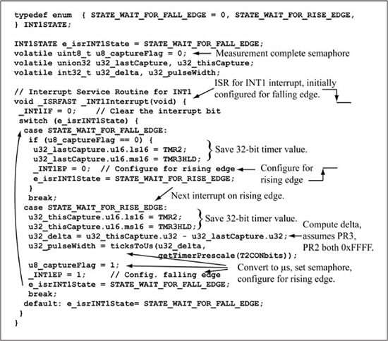
An interrupt-driven approach for pulse width measurement of the pushbutton of Figure 12.1 using Timer2/3 and the INT1 interrupt input is given in Figure 12.4. The INT1 interrupt input is assigned to the RBy port used for the pushbutton and is configured initially for a falling-edge interrupt. Figure 12.4 shows the INT1 ISR, which uses a two-state FSM, with STATE_WAIT_FOR_FALL_EDGE triggered on the switch push (falling edge). This state saves the Timer2/3 value into variable u32_lastCapture then configures the INT1 interrupt for a rising-edge trigger so that state STATE_WAIT_FOR_RISE_EDGE is entered on switch release. This state computes the delta (u32_delta) between the current Timer2/3 value and u32_lastCapture and converts this value to microseconds (u32_pulsewidth). The u8_captureFlag semaphore is set to indicate that this measurement is complete, then the INT1 interrupt is configured for a falling edge to capture the next switch press.
Figure 12.4
INT1 ISR for pulse width measurement using Timer2/3
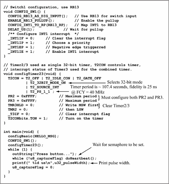
Code for configuring INT1, the input port, and Timer2/3 in addition to main() is shown in Figure 12.5. The while (1) loop in main() waits for the u8_captureFlag semaphore flag to be set then prints the pulse width. The Timer2/3 configuration code enables 32-bit mode with the T2_32BIT_MODE_ON value used in the T2CON configuration and selects a prescale of 1. Both PR2 and PR3 are set to 0xFFFF to give the maximum Timer2/3 period. At FCY = 40 MHz, one timer tick is 25 ns, and the timer period is approximately 107.4 s. While this is obviously overkill for the simple application of pushbutton pulse width measurement, this example does show the capabilities of the 32-bit timer mode in the PIC24 μC. A more common usage of the 32-bit timer mode is for scheduling long sleep times in power-sensitive applications.
Figure 12.5
Configuration code for INT1, input port, and Timer2/3
Pulse Width, Period Measurement Using Input Capture
The 32-bit timer example of the previous sections has solved the problem of long pulse width measurement, with the only drawback that this consumes two 16-bit timers. However, the dsPIC33EP128GP502 has five 16-bit timers, and two pairs of these can be used to form two independent 32-bit timers, so the resources are available if there is a need to measure a long pulse width.
However, the time measurement approaches discussed so far are not sufficient if the goal is to measure a pulse width very precisely. For example, the approach of using the INT1 interrupt as the edge trigger and reading the timer value within the ISR is faulty because the timer value is not read until several instruction cycles after the edge has occurred. Even worse, if a higher-priority ISR is executing when the active INT1 edge occurs, there is no way to predict how many instruction cycles will elapse before the INT1 ISR is executed and the timer register is read. Higher-priority interrupts are also a problem with the polling method used in Figure 12.2.
The Input Capture Module
To solve these problems, the PIC24 μC has an input capture module (see Figure 12.6) whose function is pulse width and period measurement. The problem with the methods of the previous section is that the timer value is transferred to a storage variable under instruction control when a target edge occurs. Conversely, the input capture module automatically transfers the register contents of an internal timer (ICxTMR) to a four-entry FIFO when a target edge occurs, without instruction intervention, in the same instruction cycle that the edge occurs. Captured timer values are read from the FIFO via the ICxBUF register. The dsPIC33EP128GP502 has four input capture modules with associated pin functions IC1 through IC4 that must be mapped to a remappable pin (RPx) for use. The internal timer can use any clock source that is driving one of the normal 16-bit timers (Timers 1-5). Additionally, the timer can operate in unsynchronized, synchronized, or triggered modes. In unsynchronized mode, the timer rolls over when it reaches 0xFFFF. In synchronized mode, the timer is synchronized to an external sync event that causes the timer to reset when the sync event occurs. These examples typically use one of the normal 16-bit timers to generate the sync event, which occurs when that 16-bit timer rolls over (thus, the two timers reset at the same time). In triggered mode, internal timer operation can be enabled by the same events used in synchronized mode, but this mode is not discussed in this text because of space limitations. There is also a cascade mode in which two input capture modules can be cascaded to capture a 32-bit time value (an example of this mode is given later in this chapter). The synchronized operation mode implementation in the PIC24E family can be used to provide upward compatibility with the input capture module operation of the earlier PIC24H/F families, which did not have an internal timer in the input capture module. Instead, the older input capture module captured either the TMR2 or TMR3 register value on a capture event. Most examples in this chapter use the synchronized operation mode in order to provide the broadest compatibility with dsPIC33/PIC24 CPUs.
Figure 12.7 shows the ICxCON1 configuration register details for the input capture module (this register is named ICxCON in the earlier PIC24H/F families as there is only one input capture control register in those families). A capture can be triggered on either edge, on both edges, or with a prescaler that counts 4 or 16 edge events before a timer value is captured. The setting of the ICxIF interrupt flag is configurable for every fourth, third, second, or every capture event.
Figure 12.6
Input capture block diagram

Source: Figure redrawn by author from Figure 14.1 found in the dsPIC33EPXXXGP50X datasheet (DS70657G), Microchip Technology Inc.
In the PIC24E/dsPIC33E families, there is a second control register named ICxCON2 whose function is to select either synchronized or trigger mode for the internal timer, and to select the sync/trigger events for that mode. The examples use synchronized mode with either Timer2 or Timer3 as the synchronization event source for compatibility with the PIC24H/F families, and thus the code examples assign this register in a self-documenting manner that does not require the full register definition.
Pulse Width Measurement Using Input Capture
This section discusses an interrupt-driven approach using the input capture module to solve the pulse width measurement problem of Figure 12.1. The ISR code for the IC1 input capture interrupt shown in Figure 12.8 contains a similar two-state FSM, as was used in the previous section for the 32-bit timer approach. The input capture module is configured to capture the TMR2 value on every edge and to generate an interrupt on each capture. Since you want to measure long pulse widths, but are only capturing a 16-bit timer value, the code uses the Timer2 interrupt for counting the Timer2 overflows (u16_oflowCount++) during pulse width measurement. The STATE_WAIT_FOR_FALL_EDGE state saves the capture value (u16_lastCapture) and clears the u16_oflowCount variable. The next state is STATE_WAIT_FOR_RISE_EDGE, which uses the computeDeltaTicksLong() function to compute the elapsed ticks, which are then converted to microseconds. The computeDeltaTicksLong() function is different from the previously mentioned computeDeltaTicks() function in that it has an extra parameter that is the number of timer overflows between the start and end ticks. Finally, the u8_captureFlag semaphore is set indicating that the pulse width measurement is complete. The unusual case of a simultaneous input capture with Timer2 rollover is detected by configuring the IC1 interrupt to have a higher priority interrupt than Timer2 and checking for a capture value equal to 0 and the T2IF flag being set. For this case and the falling edge capture, the u16_overflow variable is initialized to –1 instead of 0 so that the Timer2 ISR can immediately increment it, changing it to 0. For this case and the rising edge capture, the u16_overflow variable is incremented to count the timer overflow before the computeDeltaTicksLong() function is called to compute the elapsed ticks.
Figure 12.7
ICxCON1: Input capture control register

Source: Figure redrawn by author from Register 2.1 found in the dsPIC33E/PIC24E FRM Input Capture datasheet (DS70000352C), Microchip Technology Inc.
Figure 12.8
IC1 ISR for pulse width measurement using input capture

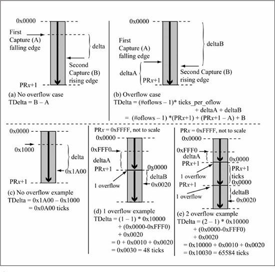
Figure 12.9 shows how the computeDeltaTicksLong() function computes the delta ticks given the starting and ending capture values and the number of timer overflows. Two cases must be considered: (a) when no timer overflow has occurred, and (b) when the number of timer overflows is greater than zero. Figures 12.9(c), (d), and (e) show numerical examples of timer delta calculations for different cases of timer overflow. Tracking timer overflows for long pulse width measurement is a better solution than using a 32-bit timer as it preserves a 16-bit timer resource for other uses.
Figure 12.9
Computing elapsed ticks given two capture values and number of timer overflows
The code for the computeDeltaTicksLong() function used in the ISR of Figure 12.8, which implements the calculations shown in Figure 12.9, is given in Listing 12.3.
Listing 12.3: Delta Time Calculation
uint32_t computeDeltaTicksLong(uint16_t u16_start, uint16_t u16_end,
                               uint16_t u16_tmrPR, uint16_t u16_oflows) {

  uint32_t u32_deltaTicks;
  uint16_t u16_delta;
  if (u16_oflows == 0) u32_deltaTicks = u16_end - u16_start;
  else {
    // Compute ticks from start to timer overflow
    u32_deltaTicks = (u16_tmrPR + 1) - u16_start;
    // Add ticks due to overflows = (overflows - 1) * ticks_per_overflow
    u32_deltaTicks += ((((uint32_t) u16_oflows) - 1) * (((uint32_t)u16_tmrPR) + 1));
    // Now add in the delta due to the last capture
    u32_deltaTicks += u16_end;
  }
  return u32_deltaTicks;
}
For completeness, note that the computation with non-zero overflows—Figure 12.9(b)—can also be used in the no overflow case—Figure 12.9(a)—if signed integers are used for ticks as follows:

Keep the differentiation between the two cases for clarity purposes. Furthermore, the non-zero overflow case of Figure 12.9(b) simplifies as follows:
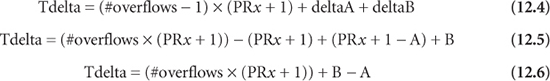
Listing 12.3 implements the original equation of Figure 12.9(b) for clarity purposes.
Figure 12.10 shows the Timer2, IC1, and switch configuration code. The main() code is not shown since it is the same in principle as in Figure 12.5. Timer2 is configured for a prescale value of 8, which gives a timer precision of 0.2 μs at FCY = 40 MHz. This means that for long pulse widths, the principal error source is clock source error.
Figure 12.10
Configuration code for Timer2, IC1, and the input port

Using Cascade Mode for 32-Bit Precision Input Capture
Cascade mode combines the internal timers of two input capture modules to form a 32-bit capture value. Figure 12.11 shows the code of Figures 12.8 and 12.10 modified to use the IC1, IC2 modules in cascade mode. Only major code differences are shown, and this example only runs on the dsPIC33E/PIC24E family members. Cascade mode uses pairs of odd/even input capture modules, with the odd module (IC1) acting the least significant timer and the even (IC2) module as the most significant timer. When the least significant timer reaches 0xFFFF, it causes the most significant timer to increment by 1. The configInputCapture() function of Figure 12.11 configures both IC2 and IC1, with IC2 being configured first in order to ensure correct operation. Both input capture modules use Timer2 as the clock source, have cascade mode enabled, capture on every edge and use synchronous mode but are not synchronized to any external 16-bit timer. Observe that both IC2 and IC1 inputs are mapped to the external pin generating the capture edges, as this causes the internal timer registers of both modules to be transferred to the capture FIFO on an active edge. The IC1Interrupt() function in Figure 12.11 differs from Figure 12.8 in that it does not track timer overflows since the input capture timers are not synchronized to a 16-bit timer. Instead, the function reads the captured IC1BUF and IC2BUF register values to form a 32-bit capture time, and computes a 32-bit pulse width once both falling and rising edges have been detected. The code uses the union32 data structure defined in Listing 12.2 and used in the 32-bit timer example of Figure 12.4. The configTimer2() function (not shown) of Figure 12.10 was changed to disable interrupts because timer overflows are not being tracked, and the main() code (not shown) is similar to that of Figure 12.5.
The input capture module is clearly the correct method to use for pulse width measurement if high precision is required by the application. In the case where the time between captured events can be greater than the timer’s period, then either tracking timer overflows is needed for computing elapsed ticks or 32-bit precision using cascade mode is required.
Period Measurement Using Input Capture
Period measurement requires time measurement between two edges of the same type, either falling-to-falling edge or rising-to-rising edge. The input capture mode select bits (ICxCON<1:0>) of Figure 12.7 that capture every 16th rising edge or every 4th rising can be used to perform an automatic averaging of the measured period. This averaging increases the effective timer precision for the period measurement. Figure 12.12 shows code for performing period measurement using IC1 and Timer2, with the assumption that a square wave is present on the IC1 input whose period does not exceed the Timer2 period. The IC1 input is configured to capture every sixteenth rising edge and to interrupt on each capture. The IC1 ISR computes the delta ticks between the last capture and the current then converts this to nanoseconds (u32_period). This value is then divided by either 16, 4, or 1 depending on the input capture mode bits (IC1CONbits.ICM) for IC1. The u8_captureFlag semaphore is then set indicating that the period measurement is ready. The main() code is not shown as it is the same principle shown in Figure 12.5.
Figure 12.11
Input capture using cascade mode

Figure 12.12
Period measurement using IC1

Application: Using Capture Mode for an Infrared Decoder
Infrared (IR) transmit and receive is a common method for wireless communication. Remote controls for televisions, VCRs, DVD players, and satellite receivers all use IR communication. IR light is just below visible light in terms of frequency within the electromagnetic spectrum. A simple scheme for IR transmit and receive is shown in Figure 12.13, in which an IR LED is turned on or off by a switch. The IR receiver is a PIN diode whose resistance varies based upon the amount of IR received, causing the output voltage to vary in the presence or absence of IR transmission.
Figure 12.13
IR transmit/receive, no modulation

Because ambient light contains an IR component, the output of the IR detector is non-zero even when no IR is being transmitted. The input to the comparator is the output of the IR detector, which is compared against a reference voltage whose value should be between the voltage output of the IR receiver in the absence or presence of IR transmission, as shown in waveform a of Figure 12.13. When Vin > Vref, the output of the comparator is VDD indicating an active IR transmission. When Vin < Vref, the output of the comparator is 0 V indicating no IR transmission. The problem with the scheme of Figure 12.13 is that a change in ambient lighting (perhaps a move from indoor lighting to outside sunshine) will change the quiescent output of the IR receiver, causing Vin either to be always above Vref (waveform b of Figure 12.13) or always below Vref.
Figure 12.14 shows an IR transmit/receive scheme that is not affected by ambient lighting conditions. To transmit IR, the switch is rapidly opened and closed to produce a modulated IR signal. A capacitor is used on the input of the comparator to block the DC component (non-changing component) of the IR detector output due to ambient lighting conditions.
Figure 12.14
IR transmit/receive with modulation

The voltage component that passes through the capacitor to the comparator input is the component that is changing due to the modulated IR input. This means that Vin is no longer affected by ambient light; the voltage seen on the capacitor output is dependent on the frequency at which the switch is opened and closed and the transmission length of one IR bit time. Typical modulation frequencies in commercial transmitters/receivers range from 36 kHz to 42 kHz with transmission bit times in the hundreds of microseconds. Commercial IR receivers such as the NJL30H/V00A (NJR Corporation) or GP1UM2xxK (SHARP Microelectronics) integrate the IR detection diode with the electronics necessary to produce a clean digital output in the presence or absence of IR transmission. Figure 12.15 shows a sample block diagram for an integrated IR receiver with three pins: VDD, ground, and Vout. The output is high in the absence of IR transmission and pulled low when a modulated IR signal is received.
Typical IR data links for remote control of home electronic systems are simplex, low-speed serial communication channels. Even though the NRZ (non-return-to-zero) encoding used for RS-232 serial data could be used for IR transmission, two other schemes known as space-width encoding and biphase encoding are commonly used for these applications. Figure 12.16(a) illustrates space-width encoding that encodes ones and zeros as different period lengths with different duty cycles.
Figure 12.15
Integrated IR receiver

Typical period lengths are in the hundreds of microseconds, with period length and duty cycle varying by manufacturer. Figure 12.16(b) shows a serial data transmission using space-width encoding in which the first bit is a start pulse, followed by space-width encoded 1s and 0s. A 0 has a period of 2T units with a 50 percent cycle, and a 1 has a period of 3T units and a 33 percent duty cycle (the duty cycles and periods were arbitrarily chosen). Decoding this serial waveform is done by measuring the time between successive falling edges to distinguish between 1s and 0s. It is not necessary to determine the duty cycle, as 1 and 0 have distinct periods. Most space-width encoding schemes use a start pulse with a period significantly longer than a 1 or 0. The periods of the start, 1, 0 bits, the number of bits sent in a transmission, and their meanings in terms of commands for the target devices are all manufacturer specific.
Figure 12.16
Space-width encoding
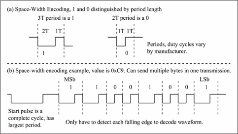
Figure 12.17(a) shows biphase encoding, which is another encoding form sometimes used with IR transmissions. In biphase encoding, each bit period is the same width with 1s and 0s distinguished by a high-to-low transition and a low-to-high transition, respectively, in the middle of the bit period. Figure 12.17(b) shows a serial data transmission using biphase encoding. Observe that the start pulse is only one-half of a bit period. One method of decoding biphase waveforms is to measure the time between both rising and falling edge transitions. If the time between two edges is one bit period, this indicates that the current bit is the complement of the previous bit. If the time between two edges is one-half period and this is the last half of the bit period, then this bit is the same as the previous bit.
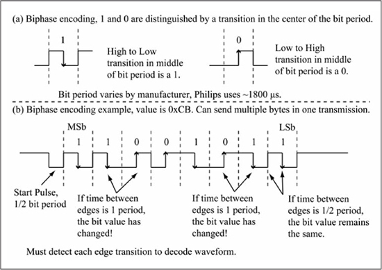
Figure 12.18(a) shows the biphase data stream for a Philips VCR remote control using the Philips RC-5 format that consists of a start pulse followed by 13 data bits. The address field specifies the target device (VCR, TV, and so on), while the command field is the particular command (play, rewind, numeral N, and so on). The first bit (the start bit) after the start pulse is always a 1, followed by the toggle bit that toggles for each new button press (if the toggle bit remains the same for several commands then the key is being held down). Figure 12.18(b) shows the biphase stream for the Play button, while Figure 12.18(c) gives the biphase stream for the numeric 3 button. Observe that when a VCR numeric button 0–9 is pressed, the 6-bit command contains the value of the numeric button. In both Figure 12.18(b) and Figure 12.18(c) the address is the same (0x05) because both of these are commands to the same device, a VCR.
Figure 12.18
Philips RC-5 command format, biphase encoded

A state machine chart for decoding the RC-5 biphase stream is given in Figure 12.19. This state machine is used in the input capture ISR, which is configured to capture and interrupt on every edge. The measured pulse width is used to determine when a half pulse or full pulse width has arrived. The START_PULSE_FALL state is triggered on the start pulse falling edge. The START_PULSE_RISE state initializes the variables needed to perform the decoding. The u1_bitEdge variable is true if the next edge is expected to contain a bit value as only transitions in the middle of a period represent a bit. The u1_bitValue variable contains the expected value of the next bit, and is initialized to 1 as the first bit after the start pulse is always a 1. A received bit is placed into u8_currentByte, with u8_bitCount tracking the number of received bits for the current byte, and u8_bitCountTotal tracking the total number of received bits. The BIT_CAPTURE state does the main work of decoding the waveform.
When an edge occurs, if a full pulse width is detected or if the u1_bitEdge variable is true, then a bit has arrived and it is placed into u8_currentByte. After seven bits have arrived the u8_currentByte is saved as it contains the start bit, toggle bit, and address bits. After thirteen total bits have arrived, the u8_currentByte is saved again as this now contains the 6-bit command value. If the IR input is 1 at this point, the last edge has arrived and so a transition is made back to START_PULSE_FALL. If the IR input is 0, the LAST_EDGE state is used to wait for the last rising edge that returns the IR input back to the idle state of 1, after which START_PULSE_FALL is entered.
Figure 12.19
State machine for RC-5 biphase decoding

The code for the IC1 ISR is given in Figure 12.20, which is a straightforward implementation of the state machine of Figure 12.19. Variables referenced within Figure 12.20 are given in Figure 12.21. The difference between a half-pulse and full-pulse is determined by comparing the current pulse width against the u16_twoThirdsPeriodTicks variable, which contains the number of ticks approximately equal to 2/3 of a full pulse width. A software FIFO as previously discussed in Chapter 10 is used for storing received IR byte values via the irFifoWrite() function.
Figure 12.20
Code for IC1 ISR that implements RC-5 biphase decoding

Software FIFO read/write functions, Timer2 configuration, and variable declarations for the RC-5 biphase decoder are given in Figure 12.21.
Figure 12.21
Support functions for RC-5 biphase decoding code

Figure 12.22 gives the IC1 configuration code, the main() function, and sample output. The while (1) loop of main() reads two bytes from the software FIFO, which are the address value (u8_x) and command value (u8_y) of a single 13-bit transmission. The toggle bit is extracted from the first byte, and the toggle, address, and command values are printed to the console. The universal remote control used to test this code sent two duplicate 13-bit transmissions for each button press. Observe that the toggle bit flipped state between the Play and numeral 3 button presses.
Figure 12.22
IC1 configuration, main(), and sample output for RC-5 biphase decoder

The Output Compare Module
In Chapter 9, a square wave was generated by using a periodic interrupt whose interrupt service routine toggled an output port, i.e., instruction execution plus timer operation generated the waveform. The PIC24E output compare module shown in Figure 12.23 provides the capability of creating hardware-generated waveforms with a high degree of precision, which is the opposite of input capture that enables precision measurement of waveform characteristics. The output compare primary and secondary registers, OCxR and OCxRS, are used as period registers in conjunction with an internal timer for setting or clearing the output compare pin (OCx), dependent on the selected operation mode. The internal timer functionality is the same as the internal timer for the input compare module in terms of unsynchronized, synchronized, or triggered modes. As with the input compare module, the examples use the internal timer of an output compare module in a synchronous mode that is synched to either Timer2 or Timer3 for compatibility with the earlier PIC24H/F families. The dsPIC33EP128GP502 contains four output compare modules, OC1-OC4, whose outputs use remappable pins.
Figure 12.23
Output compare block diagram
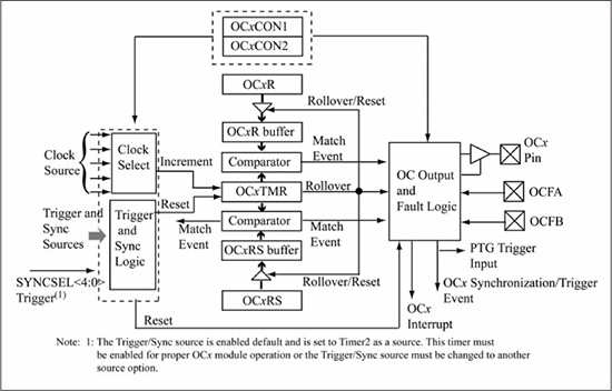
Source: Figure redrawn by author from Figure 15.1 found in the dsPIC33EEPXXXGP50X datasheet (DS70657G), Microchip Technology Inc.
Figure 12.24 shows the various operation modes of the output compare module. In the single compare single-shot modes, the OCxR register determines when the OCx output goes high or low. In toggle mode, the OCx pin is toggled for each match of OCxR against the internal timer register. In double compare single-shot mode, an OCxR register match against the internal timer triggers the rising edge of the pulse, while the falling edge is triggered by a match of OCxRS and the internal timer. Double compare continuous pulse mode has the same triggers as double compare single-shot mode, but the pulses are repeated. In edge-aligned pulse width modulation (PWM) mode, the pulse’s rising edge occurs when the internal timer value is 0, and the falling edge is triggered when the OCxR register matches the internal timer register. In center-aligned pulse width modulation (PWM) mode, the pulse’s rising edge occurs when the OCxR register matches the internal timer register, and the falling edge is triggered when the OCxRS register matches the internal timer register. In either PWM mode, the OCxR and OCxRS registers are double-buffered, which means that writes to these registers do not take effect until the next pulse. Center-aligned PWM allows the pulse to be aligned anywhere within the PWM period. The only differences between center-aligned PWM mode and double compare continuous pulse modes are the double buffering of the OCxR and OCxRS registers and that the PWM modes can use the fault control inputs. The fault control inputs (OCFA, OCFB) allow external deletion of PWM pulses by tristating the OCx output; these inputs are not covered in this textbook for space reasons. The operation modes in Figure 12.24 for the PIC 24E are upward compatible with the modes for the output compare module in the earlier PIC24H/F families.
Figure 12.24
Output compare operation

The OCxCON1control register definition is given in Figure 12.25 (this register is named OCxCON in the PIC24H/F families as these families have only one output control register). The OCTSEL<2:0> clock selection bits function the same as the clock selection bits for the input compare module. There is a second control register named OCxCON2 whose function is to select either synchronized or trigger mode for the internal timer, and to select the event source for that mode. The examples typically use synchronized mode with either Timer2 or Timer3 as the synchronization source for compatibility with the PIC24H/F families, and thus the code examples assign this register in a self-documenting manner that does not require the full register definition. The OCxCON2 register also has control bits for tristating the OCx output, inverting the OCx output, and for enabling cascade mode. Cascade mode combines two output compare modules to form a 32-bit timer that allows for very long pulse widths to be generated. See the PIC24E/dsPIC33E Family Reference Manual for further details on the OCxCON2 register and cascade mode.
Figure 12.25OCxCON1 register details
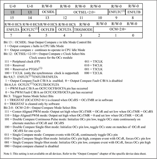
Source: Figure redrawn by author from Register 13.1 found in the dsPIC33E/PIC24E FRM Output Compare datasheet (DS70358C), Microchip Technology Inc.
Square Wave Generation
It is straightforward to create a square wave using the OCx module, as shown in Figure 12.26(a). The configOutputCapture1() function configures the OC1 module for toggle mode using Timer2 as both a clock source and for the synchronization event. The OC1R register is initialized to the number of ticks that is equal to one-quarter of the square wave period with the Timer2 period register (PR2) set to the number of ticks equal to one-half the square wave period. This causes the OC1R register to match the internal timer twice during the period, toggling the OC1 output each time, generating a square wave. Because the internal timer is synchronized to Timer2, the internal timer resets each time that Timer2 resets. The datasheet warns that the selected timer should be off during configuration of the output compare module; hence Timer2 is not enabled until after OC1 is configured. The while (1) loop in main() has no work to do since the square wave is generated by hardware and the ISR. Figure 12.26(b) shows an alternate method that does not rely on the Timer2 period register as it uses a synchronization event that resets the internal timer whenever an OC1RS match occurs. In this case, the OC1RS match replaces Timer2 rollover as the synchronization event, so OC1RS is set to the number of timer ticks that is equal to one-half the square wave period. The code in Figure 12.26(b) only works for the PIC24E/dsPIC33E families.
Figure 12.26(a)
Square wave generation using output compare

Figure 12.26(b)
Square wave generation using output compare

Pulse Width Modulation
Pulse width modulation (PWM) is a technique that varies the duty cycle of a square wave while keeping the period constant. This can be used in a variety of applications, such as varying the average current delivered to an external device. In center-aligned PWM mode, the output compare module has a period equal to the period of the sync event, which in the examples is the period of the external timer that is synchronized to the internal timer. The high pulse width is controlled by the difference in ticks between the OCxR and OCxRS registers, which simplifies to only the OCxRS register value if the OCxR register value is 0. Recall that duty cycle is the high pulse width divided by the period, multiplied by 100 percent. Thus, increasing the high pulse width increases the duty cycle. A duty cycle of 100 percent means that the PWM signal is always high. In the PIC24E/dsPIC33E families, writing to the OCxRS register changes the high pulse width in the next cycle as the OCxRS register is internally double-buffered in PWM operation. In PWM operation for the PIC24FH/F families, it is the OCxR register that controls the pulse width and the OCxRS register must be written as it serves as the double-buffer for the OCxR register. Thus, using center-aligned PWM mode with OCxR = 0 provides compatibility across the PIC24E/H/F, dsPIC33E/F families with writes to OCxRS changing the pulse width.
A PWM Example
Figure 12.27 shows an experiment illustrating how PWM can be used to control the brightness of an LED. A potentiometer is used as the input voltage for analog input RA0, whose value is read and then transformed to a pulse width for a PWM signal applied to an LED. The potentiometer is thus a convenient method for changing the duty cycle of the PWM signal. As the duty cycle of the PWM signal increases, the average current delivered to the LED increases, increasing the LED’s brightness. Of course, this may seem like a wasted effort given that the potentiometer can be directly connected to the LED for brightness control, but this demonstrates the basic principles of current control via PWM.

Figure 12.28 shows the code for implementing the LED PWM experiment. The ADC is configured for manual conversion of channel RA0 in 10-bit mode (see Chapter 11). Timer2 is configured for a period equal to the PWM period, with the Timer2 interrupt enabled. The output compare module is configured for PWM mode with no fault detection with the OC1RS register initially cleared, which initializes the OC1 output to be low. The _T2Interrupt() ISR reads the 10-bit ADC value and uses this to compute a new pulse width that is 0 to 99 percent of PR2, which is then written to OC1RS. The ISR starts a new ADC conversion before it exits. The main() code configures the ADC, Timer2, and OC1 before entering a while (1) loop that continually prints the OC1RS value for informational purposes.
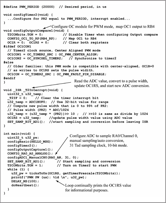
PWM Application: DC Motor Speed Control and Servo Control
This section discusses two common applications of PWM—DC motor speed control and hobby servo control.
DC Motor Speed Control
Figure 12.29 shows PWM control of a small DC motor such as that found in hobbyist robotic kits. The MOSFET is used to control the current through the motor, which can be several hundred milliamps. The gate of the MOSFET is controlled by the PWM signal; the MOSFET is turned on when the PWM signal is high, thus modulating the current flow through the motor. The average current delivered to the motor is proportional to the PWM duty cycle, and thus the motor’s torque is set by the duty cycle. The diode, known as a snubber diode, is required to protect against voltage spikes that are induced by the motor’s inductance due to the current flow interruption when the MOSFET is turned off. The switches control the rotation direction of the DC motor by reversing the current flow through the motor. The power MOSFET can be replaced by an integrated BJT Darlington pair as long as the current gain factor from input base current to collector current is high enough to supply the current required by the motor.
Figure 12.29
PWM control of a DC motor

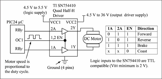
While discrete components and low-resistance analog switches can be used to implement the directional control of the DC motor of Figure 12.29, a better solution is to use a half-bridge integrated circuit that has the transistor drivers, directional control, and snubber diode protection in one package as is shown in Figure 12.30. The Texas Instruments SN754410 is a quadruple half-H driver that can supply up to 1 ampere per output with a maximum of 2 amperes total across all drivers. The 1A and 2A inputs can be used to reverse current drive in the motor, thus changing motor direction. When the enable (EN) signal is low, current drive to the motor is off.
Figure 12.30
DC motor control using half-bridge driver and PWM
Hobby Servo Control
Hobby servos, such as the Hitec HS-311 shown in Figure 12.31, are used in many applications, including robotics and remote-controlled vehicles. A servo rotates its shaft through a limited angular range whose position is specified by a PWM signal. The range of motion varies by servo manufacturer and type, with a range of –90° to +90° for the Hitec HS-311 of Figure 12.31. The 0° position is called the neutral position. The pulse width range for the HS-311 varies from a minimum high pulse time of 600 μs (–90°) to 2400 μs (+90°), with 1500 μs (0°) for neutral within a 20 ms period. An analog servo such as the HS-311 uses a DC motor with gear reduction on the shaft to slow rotation. The shaft position specified by the PWM input is maintained by an analog control circuit that uses shaft position feedback from a potentiometer. The position is maintained as long as the PWM signal is supplied and the external load on the shaft does not exceed the maximum torque ratings. If the PWM signal is removed, then the shaft freewheels, with only a small external force needed to move it. A digital servo has the same external interface as an analog servo, but uses digital controls internally that update the motor position more often than an analog servo, resulting in a servo that responds better to small position changes at the cost of increased power consumption.
Figure 12.31
DC motor control using half-bridge driver and PWM

Listing 12.4 shows the minor changes needed to the LED PWM code of Figure 12.28 to convert it to servo control. The configOutputCapture1() function has two additional lines that compute the minimum (u16_minPWTicks) and maximum (u16_maxPWTicks) PWM pulse widths in Timer2 ticks. The _T2Interrupt() ISR is modified to compute a new pulse width between these two boundary values using the conversion from the ADC. This allows the potentiometer of Figure 12.27 to control the servo’s position. The PWM period is already servo compatible with a value of 20 ms.
Listing 12.4: PWM Servo Control
#define PWM_PERIOD (20000)   // Desired period, in us
#define MIN_PW (600)          // Minimum pulse width, in us
#define MAX_PW (2400)         // Maximum pulse width, in us
uint16_t u16_minPWTicks, u16_maxPWTicks;
void configOutputCapture1(void) {
 u16_minPWTicks = usToU16Ticks(MIN_PW, getTimerPrescale(T2CONbits));
 u16_maxPWTicks = usToU16Ticks(MAX_PW, getTimerPrescale(T2CONbits));
 ... rest of the function is the same ...
}
void _ISR _T2Interrupt(void) {
  uint32_t u32_temp;
  _T2IF = 0;     // Clear the timer interrupt bit
  // Update the PWM duty cycle from the ADC value
  u32_temp = ADC1BUF0; // Use 32-bit value for range
  // Compute new pulse width using ADC value
  // ((max - min) * ADC)/1024 + min
  u32_temp = ((u32_temp*(u16_maxPWTicks - u16_minPWTicks)) >> 10) +
                 u16_minPWTicks; // >> 10 is same as divide by 1024
  OC1RS = u32_temp; // Update pulse width value
  AD1CON1bits.SAMP = 1; // Start next ADC conversion for next interrupt
}
PWM Control of Multiple Servos
The code of Listing 12.4 uses the OC1 output to directly control one servo. However, if an application requires more servos than available PWM outputs, then how is multi-servo control accomplished? The answer is to use software control of digital outputs, with the output compare ISR controlling the digital ports used for the servo outputs, as shown in Figure 12.32. The PWM period is divided into slots, with each servo assigned a slot time in which its pulse width is varied. Using a conservative slot time of 2.8 ms means that up to seven servos can be controlled in a 20 ms period (20/2.8 = 7.1). An OCx interrupt is generated for each edge of a servo’s output, with an array used for storing servo pulse widths and variables used to track the current edge and current servo. After the falling edge of the last servo’s pulse has occurred, the OCx ISR sets the next output compare interrupt to occur at the end of the 20 ms period. This approach requires only one output compare module and one timer, with the timer’s period equal to the PWM period.
Figure 12.32
Multi-servo control scheme

Listing 12.5 shows variable declarations and initialization code for the multi-servo control, with four servos used for this example. The initServos() function configures the four ports chosen for servo control and initializes them to low. The au16_servoPWidths[] array holds the pulse widths of the servos in Timer2 ticks. These entries are initialized to a value equivalent to 1500 μs, which is the servo’s neutral position. Timer2 is initialized to a period equal to 20 ms, with its interrupt disabled. The OC1 module is initialized to toggle mode, but the OC1 output is not mapped to a pin as you only care about the output compare interrupt and not the OC1 output. The OC1R register is initialized to 0, which means that the first OC1IF interrupt occurs at the first Timer2 rollover.
Listing 12.5: Initialization Code for Multi-Servo Control
#define PWM_PERIOD (20000)   // In microseconds
#define NUM_SERVOS (4)
#define SERV00 (_LATB2)
#define SERV01 (_LATB3)
#define SERV02 (_LATB13)
#define SERV03 (_LATB14)

#define MIN_PW (600)              // Minimum pulse width, in us
#define MAX_PW (2400)             // Maximum pulse width, in us
#define SLOT_WIDTH (2800)         // Slot width, in us

volatile uint16_t au16_servoPWidths[NUM_SERVOS];
volatile uint8_t u8_currentServo = 0;
volatile uint8_t u8_servoEdge = 1; // 1 = RISING, 0 = FALLING
volatile uint16_t u16_slotWidthTicks = 0;

void initServos(void) {
  uint8_t u8_i;
  uint16_t u16_initPW;

  CONFIG_RB2_AS_DIG_OUTPUT(); CONFIG_RB3_AS_DIG_OUTPUT();
  CONFIG_RB13_AS_DIG_OUTPUT(); CONFIG_RB14_AS_DIG_OUTPUT();
  u16_initPW = usToU16Ticks(MIN_PW + (MAX_PW - MIN_PW)/2,
  getTimerPrescale(T2CONbits));
  // Config all servos for half maximum pulse width
  for (u8_i = 0; u8_i < NUM_SERVOS; u8_i++) au16_servoPWidths[u8_i] = u16_initPW;
  SERV00 = 0; // All servo outputs low initially
  SERV01 = 0; SERV02 = 0; SERV03 = 0;
  u16_slotWidthTicks = usToU16Ticks(SLOT_WIDTH, getTimerPrescale(T2CONbits));
}

void  configTimer2(void) {
  T2CON = T2_OFF | T2_IDLE_CON | T2_GATE_OFF
           | T2_32BIT_MODE_OFF
           | T2_SOURCE_INT
           | T2_PS_1_256 ;  // 1 tick = 1.6 us at FCY=40 MHz
  PR2 = usToU16Ticks(PWM_PERIOD, getTimerPrescale(T2CONbits)) - 1;
  TMR2 = 0;   // Clear timer2 value
}

void configOutputCapture1(void) {
  T2CONbits.TON = 0;        // Disable Timer when configuring Output compare
  OC1R =  0;  // Initialize to 0, first match will be a first timer rollover.
  // Turn on the compare toggle mode using Timer2
  // Timer2 source, single compare toggle, just care about compare event
#ifdef OC1CON1
  OC1CON1 = OC_TIMER2_SRC |  OC_TOGGLE_PULSE;
  OC1CON2 = OC_SYNCSEL_TIMER2;   //synchronize to timer2
#else
  OC1CON = OC_TIMER2_SRC |  OC_TOGGLE_PULSE;
#endif
  _OC1IF = 0; _OC1IP = 1; _OC1IE = 1;    //enable the OC1 interrupt
}
Figure 12.33 shows the code for the OC1 ISR and main(). The variable u8_currentServo is used to track the current servo (0 to N-1), while variable u8_servoEdge is the current edge transition (1 for rising edge, 0 for falling edge). The _OC1Interrupt ISR first sets the current servo’s output high or low based on the u8_servoEdge variable. The next interrupt is then scheduled. For a rising edge, the next interrupt must occur at the falling edge of the servo output, which occurs at the current OC1R value plus the current servo’s pulse width. For the falling edge of a servo that is not the last servo, the next interrupt is the rising edge of the next servo, which is the start of the next servo’s slot and is calculated as u16_slotWidthTicks*(u8_CurrentServo + 1). For the falling edge of the last servo, the next interrupt occurs at the end of the period, so OC1R is cleared to 0. The main() code performs initialization, with the while (1) loop calling a helper function that allows a servo’s pulse width to be changed from the console for testing purposes.
Figure 12.34 shows a logic analyzer capture of the four servo outputs with the pulse widths set to different values; the period was set to 12 ms to emphasize the pulse width differences.
Figure 12.33
Multi-servo OC1 ISR and main()

Figure 12.34
Multi-servo logic analyzer capture

A PWM DAC
Notice: This section assumes some reader knowledge of low-pass RC filters; portions of this material may be difficult to understand without this background.
Another application of PWM is as a “poor man’s digital-to-analog converter” in which the PWM signal is applied to a series resistor/capacitor network to produce a DC voltage that is proportional to the PWM duty cycle. This is illustrated in Figure 12.35(a). Passing this DC voltage to a unity-gain operational amplifier provides necessary current drive and prevents the load receiving this analog voltage from affecting the PWM DAC output. In this configuration, the operational amplifier provides a gain of 1 (unity gain, voltage follower configuration), with the current draw from the RC network being negligible due to the high input impedance characteristic of this operational amplifier configuration.
Figure 12.35
A PWM digital-to-analog converter

The RC series network forms a low-pass filter that is driven by the PWM signal. The low-pass filter removes most of the high-frequency content (e.g., the switching component) of the PWM signal, leaving only the (non-switching) DC component behind, which is averaged by the capacitor storage. The average value at the low-pass filter output is the desired DAC output. Figure 12.35(c) shows a PWM signal with a 50 percent duty cycle, meaning the PWM signal is high 50% of the time. The RC filter removes the high frequency components and thus Vc = Vout = Vref/2. Figure 12.35(d) shows a result with a 12.5 percent duty cycle PWM signal where Vc = Vout = Vref/8. The voltage ripple in Figure 12.35(b) is the high frequency content of the PWM signal that has been attenuated by the low-pass filter.
Let’s examine the passive RC low-pass filter in Figure 12.35(a). The filter’s cutoff frequency in Hz is f0 = 1/(2πRC). Beyond the cutoff frequency, the filter attenuates the PWM signal frequencies at 20 dB/decade. Therefore, you can expect the PWM signal components at 10*f0 to be approximately 20 dB below those components at f0, and signal components at 100*f0 to be attenuated 20 dB below those at 10*f0 and 40 dB below those at f0. With this information, you can see that if the PWM frequency is well beyond the low-pass filter’s cutoff frequency, so switching (high frequency) components will be greatly attenuated leaving behind only the PWM’s low frequency components near DC. This filtering gives the desired result, as a signal’s DC component is equivalent to its average value. It takes a total time of five RC time constants to achieve 99.3 percent of a delta voltage change in the PWM DAC’s output voltage, with typically several PWM periods occurring during this time.
Selection of the exact RC filter values is application specific, but some general rules of thumb can be helpful in getting started. Try using f0 equal to 5–10 times the PWM DAC’s update frequency. The PWM frequency should be far into the low-pass filter’s stop band to reduce output ripple. PWM frequencies should be at least 100 times the low-pass filter cutoff so that PWM switching signal components are reduced by 40 dB or more. The PWM frequency can be reduced if the low-pass filter has stronger attenuation; multiple RC low-pass filter sections can be cascaded with each section providing an additional 20 dB/decade attenuation. Higher PWM frequencies means lower voltage ripple, but less fidelity in pulse width control. Larger RC time constants also means lower voltage ripple, but require longer to reach the new DC value after a pulse width change.
LCD displays that require positive and negative bias voltages outside of the supply rails often use a PWM signal driving a charge pump circuit to produce these voltages. If the PWM DAC is only to supply a fixed reference voltage (i.e., the PWM pulse width is not changed or changed infrequently), the previous paragraph’s recommendations can be relaxed, with the principal goal being to produce a reference voltage that meets some maximum voltage ripple specification. Equation 12.7 gives an approximate value for the RC time constant given a VDD power supply voltage (volts), desired ripple (volts), and PWM period (seconds). Equation 12.7 assumes that the RC time constant is at least 10 times greater than the PWM period.
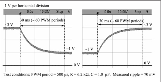
For example, if VDD = 3.3 V, PWM period = 0.5 ms (2 kHz), and ripple = 0.1 V, then RC is computed as 0.0061 s. An RC time constant of 0.0061 can be approximated by using common R, C component values of R = 6.2 kΩ, C = 1.0 μF. Figure 12.36 shows two oscilloscope captures for the design as specified. The transitions are from 3.0 V to 1.0 V and vice-versa. The measured transition time was 30 ms, which is 60 PWM periods and approximately five RC time constants. Measured ripple was 70 mV.
Time Keeping Using Timer1 and RTCC (PIC24H/F Families)
Timer1 is referred to as a Type A timer in the Family Reference Manual, and it is different from Timer2 (Type B) and Timer3 (Type C) in that it cannot be operated in a 32-bit mode but can be driven by the secondary oscillator (external pins SOSCI and SOSCO). Timer2 and Timer3 can be driven by an external clock pin (TxCK), but not by the secondary oscillator. The secondary oscillator is a common feature found on the PIC24H/F families but is on very few devices in the PIC24E family (it is not included in the dsPIC33EP128GP502 CPU used in the Chapter 8 reference system). One use for the secondary oscillator is for real-time clock keeping (seconds, minutes, and hours) using a 32.768 kHz watch crystal. An interrupt occurs every second using this clock frequency with a period register of 0x7FFF (the period is 0x7FFF + 1 = 0x8000 = 32768 timer ticks, which is 1 second for a 32.768 kHz clock). Real time can be kept by incrementing a variable on each interrupt. See the Family Reference Manual [19] for details on the Timer1 configuration register and block diagram, as it is very similar to Timer2.
Figure 12.37 shows code that assumes a 32.768 kHz crystal on the secondary oscillator, with the _T1Interrupt ISR incrementing the u16_seconds variable on each interrupt. The configTimer1() function configures Timer1 for an external clock, prescale of 1, PR1 value of 0x7FFF, and the interrupt is enabled. Timer1 is also configured to remain operational during sleep mode by using the T1_IDLE_CON mask. The main() function enables the secondary oscillator amplifier by setting the SOSCEN bit (OSCCON<2>) using the PIC24 compiler’s __builtin_write_OSCCONL function. This built-in function does the necessary unlock sequence required to make changes to the OSCCON register. The external crystal will not oscillate if this amplifier is disabled. The while (1) loop prints the u16_seconds variable, then sleeps. Because Timer1 is using an external clock and is configured for operation during sleep, its interrupt can be used to wake the processor from sleep mode.
Figure 12.37
Keeping real time with Timer1

The Real-Time Clock Calendar Module
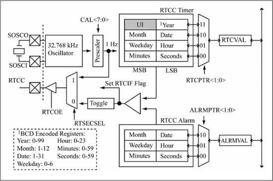
There is more to time keeping than just keeping track of seconds, and the Real-Time Clock Calendar (RTCC) module [42] on some PIC24F/H family members and a few PIC24E family members can track seconds, minutes, hours, days of the week, days of the month, months, and years using an external 32.768 kHz clock. The code example in this section is for the RTCC module found in the PIC24H family and was tested on a PIC24HJ64GP502 CPU. The RTCC module capabilities are fairly extensive, and this section only highlights the basic features of the module. Figure 12.38 shows the RTCC block diagram; observe that the clock/calendar time-keeping registers are each 8 bits wide and BCD encoded (see Chapter 7). Besides toggling the RTCC output, the alarm feature allows an interrupt to be generated on a match of the clock registers with the alarm registers.
Figure 12.38
RTCC block diagram
Source: Figure redrawn by author from Figure 37.1 found in the PIC24H FRM datasheet (DS70310A), Microchip, Technology Inc.
The main control register for the RTCC is named RCFGCAL (see the FRM [42] for details). The RTCPTR<1:0> (RCFGCAL<9:8>) pointer bits are used to access the RTCC registers using 16-bit accesses to the RTCVAL register. When the RTCPTR<1:0> bits are initialized to 11, the first 16-bit access goes to UI:Year, after which RTCPTR is auto decremented so that the next access is to Month:Date, and so on. Furthermore, accesses to the RTCC registers require a special unlock sequence similar to that required for the OSCCON register. When writing to the RTCC registers, it is recommended by the FRM that the module be disabled. A status bit named RTCSYNC (RCFGCAL<12>) is true when register rollover is 32 clock edges (~ 1 ms) from occurring; this is useful for determining when it is safe to read register values.
Figure 12.39 shows the first part of a test program for the RTCC. The unionRTCC union contains two declarations, a struct named u8 that provides byte access to the RTCC registers and a uint16_t array named regs that allows 16-bit accesses to the registers. The getDateFromUser() function is used to read the initial date and time settings from the console. The getBCDvalue(char* sz_1) utility function is called by getDateFromUser() for each date/time component. The sz_1 parameter is a string used to prompt the user to enter a two-digit ASCII decimal value that is placed into sz_buff. This ASCII decimal string is then converted to binary by the sscanf function, which is then converted to a BCD 8-bit value that is returned by the function. Each of the BCD date/time components read by getDateFromUser() are stored in their appropriate u8 member of the global variable u_RTCC, which is of type unionRTCC.
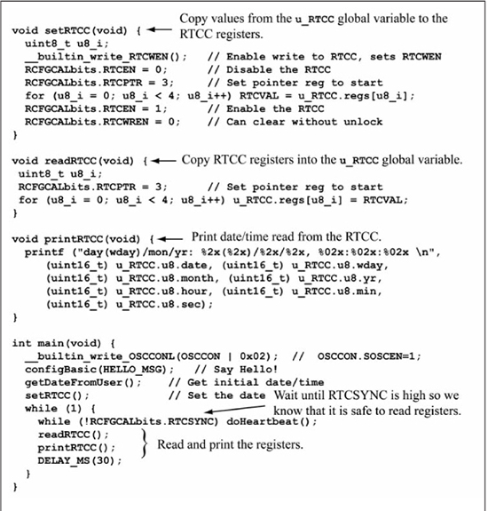
Figure 12.40 shows the second part of the RTCC test code. The setRTCC() function copies data from the global variable u_RTCC into the RTCC registers. The builtin_write_RTCWEN() function provided by the PIC24 compiler does the unlock sequence for the RTCC registers and sets the RTCWEN bit, allowing register modification. The RTCEN bit is cleared, disabling the module, which is suggested by the FRM during register updates. The RTCPTR bits are set to 3, and a loop does four 16-bit writes that copies data from u_RTCC to entry register RTCVAL. As mentioned earlier, each 16-bit write auto-decrements the RCCPTR bits, so each write goes to a different register pair in the RTCC. The end result is that the different time/date components of u_RTCC are written to the correct RTCC registers. Before exiting, the RTCC module is enabled by setting RTCEN, and register writes are disabled by clearing RTCWREN. The readRTCC() function does the reverse of writeRTCC(); data is copied from the RTCC registers into the u_RTCC global variable. The printRTCC() function prints time/data components from u_RTCC to the console. The main() function sets the initial time/date setting for the RTCC using the getDateFromUser() and setRTCC() functions. The while (1) loop is then entered, which monitors the RTSYNC bit to determine when it is safe to read the RTCC registers without a date or time rollover occurring during the read, which could return inconsistent data. After the RTSYNC bit is set, the RTCC registers are read and printed to the console using the readRTCC() and printRTCC() functions.
Figure 12.39
RTCC example code (part 1)

Two tests of the RTCC code are shown in Figure 12.41. The left-side console output shows the data rolling over from midnight of December 31, 2015, to the next day, which is the beginning of a new year. The right-side test shows a leap year test of rolling over from February 28 to February 29 in the year 2016.
Figure 12.40
RTCC example code (part 2)

Summary
All of the Timerx subsystems of the PIC24 μC family, designated as Type A (Timer1), Type B (Timer2, 4, 6, and so on), and Type C (Timer3, 5, 7, and so on) are 16-bit timers that can be clocked from an internal (FCY) or external source and have a prescaler with possible values of 1, 8, 64, and 256. Additionally, the Type B and Type C timers can be combined to form a single 32-bit timer. The input capture module is used for performing accurate pulse width or period measurement. Input capture was used to decode a biphase-encoded IR signal generated by a universal remote control. The output capture mode can be used for hardware generation of various types of pulse trains, including pulse width modulation, which varies the duty cycle of a fixed period square wave. Applications of PWM include servo positioning and DC motor speed control. The secondary oscillator found on some members of the PIC24 μC family can be used with a 32.768 kHz watch crystal and Timer1 for simple timekeeping. Complete time/date timekeeping is provided by the RTCC module found on some members of the PIC24 μC family.
Review Problems
1. Refer to Figure 12.9 and assume a 40 MHz FCY and a prescale value of 8 for Timer2 operating in 16-bit mode, with PR2 = 0xFFFF. Assume that the first input capture has a value of 0xA000 and the second input capture a value of 0x1200, with one Timer2 overflow between captures. How much time has elapsed between the captures? Give the answer in microseconds.
2. Refer to Figure 12.9 and assume a 40 MHz FCY and a prescale value of 8 for Timer2 operating in 16-bit mode, with PR2 = 0xFFFF. Assume that the first input capture has a value of 0x0800 and the second input capture a value of 0xE000, with three Timer2 overflows between captures. How much time has elapsed between the captures? Give the answer in milliseconds.
3. Assume Timer2/3 operating in 32-bit mode with a 20 MHz FCY and a prescale value of 64. How long does it take for this timer to overflow? Give the answer to the nearest second.
4. Assume Timer2/3 operating in 32-bit mode with a 20 MHz FCY and a prescale value of 256. How many Timer2/3 ticks are contained in two seconds?
5. Assume a 40 MHz FCY and a prescale value of 8 for Timer2 operating in 16-bit mode. Input capture has measured 2,000 ticks between the rising edges of a square wave. What is the square wave’s frequency in kHz?
6. Assume a 16 MHz FCY and a prescale value of 1 for Timer2 operating in 16-bit mode. You want to use input capture to measure the frequency of a square wave. What is the highest frequency that can be measured assuming that you want at least four ticks per square wave period?
7. Assume a 20 MHz FCY and a prescale value of 8 for Timer2 operating in 16-bit mode. Also assume that an output compare module has been configured for pulse width modulation using a 10 ms period. What OCxRS register value is required to produce a pulse width of 5 ms?
8. Assume a 40 MHz FCY and a prescale value of 64 for Timer2 operating in 16-bit mode. Also assume that an output compare module configured for pulse width modulation using a 20 ms period is being used to control an HS-311 servo. What OCxRS register value is required to produce to position the servo arm at 45°?
9. Assume a 16 MHz FCY and a prescale value of 256 for Timer2 operating in 16-bit mode. Also assume that an output compare module configured for pulse width modulation using a 15 ms period is being used to control the speed of a DC motor using the scheme of Figure 12.30. What OC x RS register value is required to run the motor at 1/3 full speed (assume a linear relationship between DC motor speed and pulse width)?
10. Assume an input capture pin is being used to monitor the U1RX pin. Describe an approach for computing the baud rate of a connection assuming that a few 0x55 characters are sent to the port. (You do not have to write code, just describe the approach you would use and why it would work.)