CHAPTER 1
NUMBER SYSTEM AND DIGITAL LOGIC REVIEW
This chapter reviews number systems, Boolean algebra, logic gates, combinational logic gates, combinational building blocks, sequential storage elements, and sequential building blocks.
Learning Objectives
After reading this chapter, you will be able to:
![]() Create a binary encoding for object classification.
Create a binary encoding for object classification.
![]() Convert unsigned decimal numbers to binary and hex representations and vice versa.
Convert unsigned decimal numbers to binary and hex representations and vice versa.
![]() Perform addition and subtraction on numbers in binary and hex representations.
Perform addition and subtraction on numbers in binary and hex representations.
![]() Identify NOT, OR, AND, NOR, NAND, and XOR logic functions and their symbols.
Identify NOT, OR, AND, NOR, NAND, and XOR logic functions and their symbols.
![]() Evaluate simple Boolean functions.
Evaluate simple Boolean functions.
![]() Describe the operation of CMOS P and N transistors.
Describe the operation of CMOS P and N transistors.
![]() Identify the CMOS transistor-level implementations of simple logic gates.
Identify the CMOS transistor-level implementations of simple logic gates.
![]() Compute clock period, frequency, and duty cycle given appropriate parameters.
Compute clock period, frequency, and duty cycle given appropriate parameters.
![]() Identify common combinational building blocks.
Identify common combinational building blocks.
![]() Identify common sequential building blocks.
Identify common sequential building blocks.
![]() Translate a character string into ASCII encoded data, and vice versa.
Translate a character string into ASCII encoded data, and vice versa.
Binary number system representation and arithmetic is fundamental to all computer system operations. Basic logic gates, CMOS (Complementary Metal Oxide Semiconductor) transistor operation, and combinational/sequential building block knowledge will help your comprehension of the diagrams found in datasheets that describe microprocessor subsystem functionality. A solid understanding of these subjects ensures better understanding of the microprocessor topics that follow in later chapters.
Using Binary Data
Binary logic, or digital logic, is the basis for all computer systems built today. Binary means two, and many concepts can be represented by two values: true/false, hot/cold, on/off, 1/0, to name a few. A single binary datum whose value is 1 or 0 is referred to as a bit. Groups of bits are used to represent concepts that have more than two values. For example, to represent the concepts hot/warm/cool/cold, two or more bits can be used as shown in Table 1.1.
Table 1.1: Digital Encoding Examples
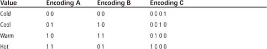
To encode n objects, the minimum number of bits required is k = ceil(log2 n), where ceil is the ceiling function that takes the nearest integer greater than or equal to log2 n. For the four values in Table 1.1, the minimum number of bits required is ceil(log2 (4)) = 2. Both encoding A and encoding B use the minimum number of bits, but differ in how codes are assigned to the values. Encoding B uses a special encoding scheme known as Gray code, in which adjacent table entries only differ by at most one bit position. Encoding C uses more than the minimum number of bits; this encoding scheme is known as one-hot encoding, as each code only has a single bit that is a 1 value.
Encoding A uses binary counting order, which means that the code progresses in numerical counting order if the code is interpreted as a binary number (base 2). In an unsigned binary number, each bit is weighted by a power of two. The rightmost bit, or least significant bit (LSb), has a weight of 20, with each successive bit weight increasing by a power of two as you move from right to left. The leftmost bit, the most significant bit (MSb), has a weight of 2n – 1 for an n-bit binary number. A lowercase “b” is purposefully used in the LSb and MSb acronyms since the reference is to a single bit; the use of an uppercase “B” in LSB and MSB acronyms is discussed in Chapter 3.
The formal term for a number’s base is radix. If r is the radix, then a binary number has r = 2, a decimal number has r = 10, and a hexadecimal number has r = 16. In general, each digit of a number of radix r can take on the values 0 through r – 1. The least significant digit (LSD) has a weight of r0, with each successive digit increasing by a power of r as you move from right to left. The leftmost digit, the most significant digit (MSD), has weight of rn – 1, where n is the number of digits in the number. For hexadecimal (hex) numbers, letters A through F represent the digits 10 through 15, respectively.
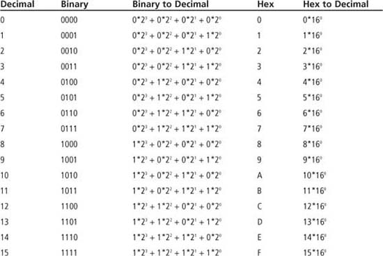
Decimal, binary, and hexadecimal numbers are used extensively in this book. If the base of the number cannot be determined by context, a 0x is used as the radix identifier for hex numbers (i.e., 0x3A) and 0b for binary numbers (i.e., 0b01101000). No radix identifier is used for decimal numbers. Table 1.2 lists the binary and hex values for the decimal values 0 through 15. Note that 4 bits are required to encode these 16 values since 24 = 16. The binary and hex values in Table 1.2 are given without radix identifiers. The * symbol in Table 1.2 is a multiplication operation; other symbols used in this book for multiplication are × (a × b) and · (a · b) with the usage made clear by the context.
Table 1.2: Binary Encoding for Decimal Numbers 0–15
A binary number of n bits can represent the unsigned decimal values of 0 to 2N – 1. A common size for binary data is a group of eight bits, referred to as a byte. A byte can represent the unsigned decimal range of 0 to 255 (0x00 to 0xFF in hex). Groups of bytes are often used to represent larger numbers; this topic is explored in Chapter 5. Common powers of two are given in Table 1.3. Powers of two that are evenly divisible by 210 can be referred to by the suffixes Ki (kibi, kilobinary, 210), Mi (mebi, megabinary, 220), and Gi (gibi, gigabinary, 230). The notation of Ki, Mi, and Gi is adopted from IEEE Standard 1541-2002, which was created to avoid confusion with the suffixes k (kilo, 103), M (mega, 106), and G (giga, 109). Thus, the value of 4,096 can be written in the abbreviated form of 4 Ki (4 * 1 Ki = 22 * 210 = 212 = 4096 = 4.096 k). However, be aware that the terminology of this IEEE standard is not in widespread use yet. The terms kBytes and MBytes are commonly used when referring to memory sizes and these mean the same as KiBytes and MiBytes.
Table 1.3: Common Powers of Two
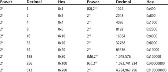
Sample Question: What is the largest unsigned decimal number that can be represented using a binary number with 16 bits?
Answer: From Table 1.3, you can see that 216 = 65,536, so 216 – 1 = 65,535.
Unsigned Number Conversion
To convert a number of any radix to decimal, simply multiply each digit by its corresponding weight and sum the result. The example that follows shows binary-to-decimal and hex-to-decimal conversion:
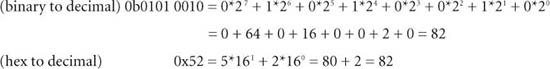
To convert a decimal number to a different radix, perform successive division of the decimal number by the radix; at each step the remainder is a digit in the converted number, and the quotient is the starting value for the next step. The successive division ends when the quotient becomes less than the radix. The digits of the converted number are determined rightmost to leftmost, with the last quotient being the leftmost digit of the converted number. The following sample problem illustrates the successive division algorithm.
Sample Question: Convert 435 to hex.
Answer:
Step 1: 435/16 = 27, remainder = 3 (rightmost digit).
Step 2: 27/16 = 1, remainder = 11 = 0xB (next digit).
Step 3: 1 < 16, so leftmost digit = 1.
Final answer: 435 = 0x1B3
To check your work, perform the reverse conversion:
0x1B3 = 1*162 + 11*161 + 3*160 = 1*256 + 11*16 + 3*1 = 256 + 176 + 3 = 435
Hex to Binary, Binary to Hex
Hex can be viewed as a shorthand notation for binary. A quick method for performing binary-to-hex conversion is to convert each group of four binary digits (starting with the rightmost digit) to one hex digit. If the last (leftmost) group of binary digits does not contain four bits, then pad with leading zeros to reach four digits. Converting hex to binary is the reverse procedure of replacing each hex digit with four binary digits. The easiest way to perform decimal-to-binary conversion is to first convert to hex then convert the hex number to binary. This involves fewer division operations and hence fewer chances for careless error. Similarly, binary-to-decimal conversion is best done by converting the binary number to a hex value, and then converting the hex number to decimal. The following examples illustrate binary-to-hex, hex-to-binary, and decimal-to-binary conversion.
Sample Question: Convert 0b010110 to hex.
Answer: Starting with the rightmost digit, form groups of four: 01 0110. The leftmost group has only two digits, so pad this group with zeros as: 0001 0110. Now convert each group of four digits to hex digits (see Table 1.2):
0b 0001 0110 = 0x16.
Sample Question: Convert 0xF3C to binary.
Answer: Replace each hex digit with its binary equivalent:
0xF3C = 0b 1111 0011 1100
Sample Question: Convert 243 to binary.
Answer: First, convert 243 to hex:
Step 1: 243/16 = 15, remainder 3 (rightmost digit).
Step 2: 15 < 16, so leftmost digit is 0xF (15). Hex result is 0xF3.
243 = 0xF3 = 0b 1111 0011 (final answer, in binary)
Check: 0xF3 = 15*16 + 3 = 240 + 3 = 243
Binary and Hex Arithmetic
Addition, subtraction, and shift operations are implemented in some form in most digital systems. The fundamentals of these operations are reviewed in this section and revisited in Chapters 3 and 4 when discussing basic computer operations.
Binary and Hex Addition
Adding two numbers, i + j, in any base is accomplished by starting with the rightmost digit and adding each digit of i to each digit of j, moving right to left. If the digit sum is less than the radix, the result digit is the sum and a carry of 0 is used in the next digit addition. If the sum of the digits is greater than or equal to the radix, a carry of 1 is added to the next digit sum, and the result digit is computed by subtracting r from the digit sum. For binary addition, these rules can be stated as:
![]() 0 + 0 = 0, carry = 0
0 + 0 = 0, carry = 0
![]() 0 + 1 = 1, carry = 0
0 + 1 = 1, carry = 0
![]() 1 + 0 = 1, carry = 0
1 + 0 = 1, carry = 0
![]() 1 + 1 = 0, carry = 1
1 + 1 = 0, carry = 1
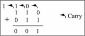
Figure 1.1 shows a digit-by-digit addition for the numbers 0b110 + 0b011. Note that the result is 0b001 with a carry-out of the most significant digit of 1. A carry-out of the most significant digit indicates that the sum produced unsigned overflow; the result could not fit in the number of available digits. A carry-out of the most significant digit is an unsigned error indicator if the numbers represent unsigned integers. In this case, the sum 0b110 + 0b011 is 6 + 3 with the correct answer being 9. However, the largest unsigned integer that can be specified in three bits is 23 – 1, or 7. The value of 9 is too large to be represented in three bits, and thus the result is incorrect from an arithmetic perspective, but is correct by the rules of binary addition. This is known as the limited precision problem; only increasing the number of bits used for binary encoding can increase the number range. You’ll study this problem and the consequences of using more or fewer bits for number representation in later chapters.
Figure 1.1
Binary addition example
Sample Question: Compute 0x1A3 + 0x36F.
Answer: A digit-by-digit addition for the operation 0x1A3 + 0x36F is as follows. The rightmost result digit is formed by adding:
0x3 (3) + 0xF (15) = 18
Note the digit sum is greater than 16, so a carry of 1 is produced and the rightmost result digit is computed by subtracting the radix, or:
18 – 16 = 2 = 0x2
The middle digit sum is then:
0xA (10) + 0x6 (6) + 1 (carry) = 17
This digit sum is greater than 16, so this produces a carry of 1 with the middle digit computed as:
17 – 16 = 1 = 0x1
The leftmost digit sum is:
0x1 + 0x3 + 0x1 (carry) = 0x5
The result is then 0x1A3 + 0x36F = 0x512. Converting each number to decimal before summing, or 419 + 879 = 1298, checks this result. Verifying that 0x36F – 0x512 = 0x1A3 also checks this result, but this requires reading the next section on subtraction!
Binary and Hex Subtraction
Subtracting two numbers, i – j, in any base is accomplished by starting with the rightmost digit and subtracting each digit of j from each digit of i, moving right to left. If the i digit is greater or equal to the j digit, then the resulting digit is the subtraction i – j, with a borrow of 0 used in the next digit subtraction. If the i digit is less than the j digit, then a borrow of 1 is used in the next digit subtraction, and the resulting digit is formed by i + r – j (the current i digit is increased by a weight of r). For binary subtraction, these rules can be stated as:
![]() 0 – 0 = 0, borrow = 0
0 – 0 = 0, borrow = 0
![]() 0 – 1 = 1, borrow = 1
0 – 1 = 1, borrow = 1
![]() 1 – 0 = 1, borrow = 0
1 – 0 = 1, borrow = 0
![]() 1 – 1 = 0, borrow = 0
1 – 1 = 0, borrow = 0
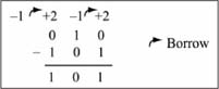
Figure 1.2 shows a digit-by-digit subtraction for the value 0b010 – 0b101. This operation produces a result of 0b101, and a borrow-out of the most significant digit of 1. If interpreted as unsigned numbers, the operation is 2 – 5 = 5, which is incorrect. A borrow-out of the most significant digit of 1 indicates an unsigned underflow; the correct result is a number less than zero. But in unsigned numbers, there is no number less than zero, so the result is incorrect in an arithmetic sense; the operation is perfectly valid, however. A binary representation for signed integers is needed to interpret the binary result correctly; this topic is saved for Chapter 5.
Figure 1.2
Binary subtraction example
The subtraction A – B can also be performed by the operation A + ~B + 1, where the operation ~B is called the one’s complement of B and is formed by taking the complement of each bit of B.
In review, the complement of a bit is its logical inverse or opposite, so the complement of 0xAE50 = 0b 1010 1110 0101 0000 is 0b 0101 0001 1010 1111 = 0x51AF. As an example of binary subtraction, consider the previous operation of 0b010 – 0b101. The one’s complement of 0b101 is 0b010. The subtraction can be rewritten as:
A + ~B + 1 = 0b010 + (0b010 + 0b001) = 0b010 + 0b011 = 0b101
This is the same result obtained when binary subtraction rules were used. The value ~B + 1 is called the two’s complement of B; this is discussed in more detail in Chapter 5, when signed integer representation is covered.
Sample Question: Compute 0xA02 – 0x5C4.
Answer: A digit-by-digit hex subtraction for the operation 0xA02 – 0x5C4 is as follows. The rightmost subtraction of 0x2 – 0x4 requires a borrow from the next digit, so the rightmost digit calculation becomes:
2 + 16 – 4 = 14 = 0xE
The middle digit calculation becomes 0x0 – 0xC – 0x1 (borrow). This requires a borrow from the next (leftmost) digit, so this calculation becomes:
16 + 0 – 12 – 1 = 3 = 0x3
The leftmost digit calculation is:
0xA – 0x5 – 0x1 (borrow) = 10 – 5 – 1 = 4 = 0x4
Thus, the final result is 0xA02 – 0x5C4 = 0x43E. As always, this result can be checked by verifying that 0x5C4 + 0x43E = 0xA02 (and yes, it is correct!).
Shift Operations
A right shift of a binary value moves all of the bits to the right by one position and shifts a new bit value into the MSb. Shifting in a value of 0 is equivalent to dividing the binary value by two if the binary value represents an unsigned number (the differences between unsigned and signed number representation are discussed in Chapter 5). For example, using a 0 value for the bit shifted into the MSb, the unsigned binary value 0b1100 (12) shifted to the right by one position is 0b0110 (6). If this value is shifted to the right once more, the new value is 0b0011 (3). In this book, operators from the C language are used for expressing numerical operations. The C language operator for a right shift is >>, where A >> 1 reads “A shifted to the right by one bit.”
A left shift of an unsigned binary value moves all of the bits to the left by one position, and shifts a new bit value into the LSb. If the new bit shifted in is a 0, this is equivalent to multiplying the binary value by two. For example, using a 0 value for the bit shifted into the LSb, the binary value 0b0101 (5) shifted to the left by one position is 0b1010 (10). If this value is shifted to the left once more, the new value is 0b0100 (4). The value 4 is not 10 * 2; the correct result should be 20. However, the value 20 cannot fit in 4 bits; the largest unsigned value represented in 4 bits is 24 – 1 = 15. In this case, the bit shifted out of the MSb is a 1; when this happens, unsigned overflow occurs for the shift operation and the new value is incorrect in an arithmetic sense. The C language operator for a left shift is <<, where A << 1 reads “A shifted to the left by one bit.” Figure 1.3 gives additional examples of left and right shift operations.
If an n-bit value is shifted to the left or right n times, with 0 used as the shift-in value, the result is zero, as all bits become 0. When shifting a hex value, it is best to convert the hex number to binary, perform the shift, then convert the binary number back to hex.
Figure 1.3
Shift operation examples
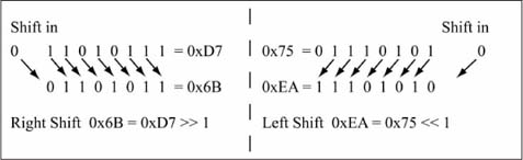
Sample Question: What is the new value of 0xA7 >> 2 assuming the MSb is filled with 0s?
Answer: The value 0xA7 = 0b1010 0111, so 0xA7 >> 1 = 0b0101 0011. Shifting this value to the right by one more gives 0b0101 0011 >> 1 = 0b0010 1001 = 0x29. Therefore, 0xA7 >> 2 = 0x29.
Combinational Logic Functions
Boolean algebra defines properties and laws between variables that are binary valued. The basic operations of Boolean algebra are NOT, OR, and AND, whose definitions are:
![]() NOT(A): Is 1 if A = 0; NOT(A) is 0 if A = 1 (the output is said to be the complement or inverse of the input).
NOT(A): Is 1 if A = 0; NOT(A) is 0 if A = 1 (the output is said to be the complement or inverse of the input).
![]() AND(A1, A2, ... An): Is 1 only if all inputs A1 through An have a value = 1.
AND(A1, A2, ... An): Is 1 only if all inputs A1 through An have a value = 1.
![]() OR(A1, A2, ... An): Is 1 if any input A1 through An has a value = 1.
OR(A1, A2, ... An): Is 1 if any input A1 through An has a value = 1.
The C language operators for bitwise complement (~), AND (&), OR (|) are used in this book for logic operations. Thus, NOT(A) = ~A, AND(A, B) = A & B, and OR(A, B) = A | B, where the Boolean variables have values of either 0 or 1. Logic operations are also defined by truth tables and by distinctively shaped symbols. A truth table has all input combinations listed in binary counting order on the left side, with the output value given on the right side of the table. Figure 1.4 lists the two-input truth tables and shape distinctive symbols for the NOT, AND, OR, NAND, NOR, and XOR (exclusive-OR) logic functions.
Figure 1.4
Truth table, logic symbols for basic two-input logic gates
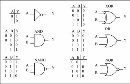
A NAND function is an AND function whose output is complemented (i.e. inverted); similarly, a NOR function is an OR function whose output is complemented. An XOR function is defined by the truth table shown in Figure 1.4 or can be expressed using NOT, AND, OR operators, as shown in Equation 1.1. The C language operator for XOR is ^, thus XOR(A, B) = A ^ B. Logically stated, XOR(A, B) is 1 if A is not equal to B, and 0 otherwise.
The distinctively shaped symbol for a Boolean logic function is also referred to as the logic gate for the Boolean operation. A network of logic gates is an alternative representation of a Boolean equation. Figure 1.5 shows the Boolean equation of the XOR function drawn as a logic network using two-input gates.
Figure 1.5
AND/OR logic network for the XOR function
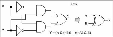
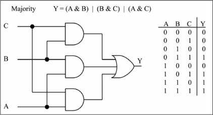
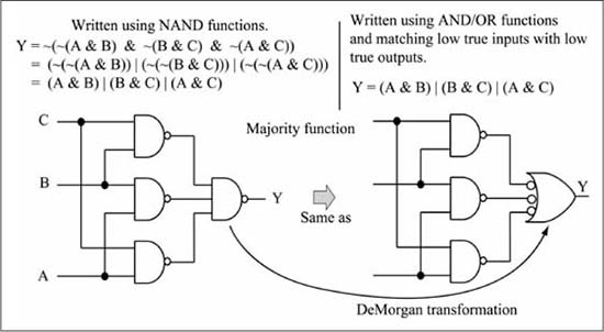
Figure 1.6 gives the AND/OR network, Boolean equation, and truth table for a three-input majority function; so named because the output is a 1 only when a majority of the inputs are a 1.
Figure 1.6
AND/OR logic network for the three-input majority function
An important law relating to AND/OR/NOT relationships is known as DeMorgan’s Law, with its forms shown in Figure 1.7. A “circle” or “bubble” on a gate input means that input is complemented. Note that a NAND function can be replaced by an OR function with complemented inputs (Form 1), while a NOR function can be replaced by an AND function with complemented inputs (Form 2). Forms 1 and 2 of DeMorgan’s Law can be validated by comparing the truth tables of the left and right sides, while forms 3 and 4 follow from substitution of forms 1 and 2. Complemented inputs/outputs are also known as low-true inputs/outputs, and uncomplemented inputs/outputs are called high-true inputs/outputs. Through DeMorgan’s Law and the high-true, low-true terminology, the NAND gate of Figure 1.7 can be viewed as either an AND gate with high-true inputs and a low-true output, or as an OR gate with low-true inputs and a high-true output.
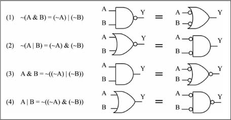
Figure 1.7
DeMorgan’s Law and the high-true, low-true terminology
DeMorgan’s Law can be used to replace all of the AND/OR gates in Figure 1.6 with NAND gates, as shown in Figure 1.8. This is important as the physical implementation of a NAND gate using Complementary Metal Oxide Semiconductor (CMOS) transistors is faster and has fewer transistors than either an AND gate or an OR gate.
Figure 1.8
NAND/NAND logic network for a three-input majority function
Logic Gate CMOS Implementations
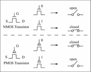
CMOS (pronounced as “see-moss”) transistors are the most common implementation method used today for logic gates, which form the building blocks for all digital computation methods. You’ll review the basics of CMOS transistor operation here and revisit the topic in Chapter 8 when discussing computer input/output. The “C” in CMOS stands for complementary, which refers to the fact that there are two types of MOS (“moss”) transistors, N and P, whose operation is complementary to each other. Each MOS transistor type has four terminals, three of which are: Gate (g), Source (s), and Drain (d). The fourth terminal is the substrate or bulk terminal, which can be ignored in this discussion. For the purposes here, you will view a MOS transistor as an ideal switch whose operation is controlled by the gate terminal. The switch is either closed (a connection exists between source and drain, so current flows between source and drain) or open (no connection exists between source and drain, so there is no current flow between source and drain). An N-type transistor is open when the gate has a logic 0 and closed when the gate has a logic 1. A P-type transistor has complementary operation; a 1 on the gate opens the switch, a 0 closes the switch. A logic 1 is physically represented by the power supply voltage of the logic gate, or VDD. The power supply voltage used for a CMOS logic gate can vary widely, from 5 V (Volts) down to approximately 1.0 V. A logic 0 is physically represented by the system ground, or GND, which has a voltage value of 0 V (VSS is also a common designation for ground). Figure 1.9 illustrates P and N transistor operation.
Figure 1.9
CMOS transistor operation
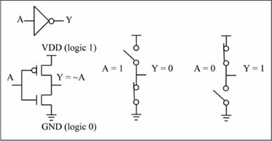
Multiple CMOS transistors can be connected to form logic gates. Figure 1.10 shows the simplest CMOS logic gate, which is the NOT function, or inverter. When the input value is 0, the upper switch (the P transistor) is closed, while the lower switch (the N transistor) is open. This connects the output to VDD, forcing the output to a 1. When the input value is 1, the upper switch is open, while the lower switch is closed. This connects the output to GND, forcing the output to a 0. Thus, for an input of 0 the output is 1; for an input of 1 the output is a 0, which implements the NOT function.
Figure 1.10
CMOS inverter operation
Note that a buffer function Y = A is formed if two inverters are tied back to back as shown in Figure 1.11. It would seem that a better way to build a buffer is to switch the positions of the N and P transistors of the inverter, thus implementing the buffer with only two transistors instead of four. However, for physical reasons best left to an electronics book, a P transistor is always used to pass a 1 value, while an N transistor is always used to pass a 0 value. Thus, in digital logic, a P transistor is never tied to ground, and an N transistor is never tied to VDD, so the two-transistor buffer shown in Figure 1.11 is illegal. Because of the rule given in the previous sentence, a noninverting CMOS logic function always takes two stages of inverting logic.
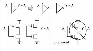
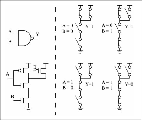
Figure 1.12 shows the transistor configuration and operation of a two-input CMOS NAND gate. Note that the output is connected to ground (both bottom transistors are closed) only when both inputs are a 1 value. Also observe that no combination of inputs provides a direct path between VDD and GND; this would cause a short (low resistance path) between VDD and GND, resulting in excessive current flow. The lack of a direct path from VDD to GND means that CMOS gates have a very low power consumption when they are not switching, which is an important advantage of this technology. The four-transistor configuration for a CMOS NOR gate is left as an exercise for the review problems.
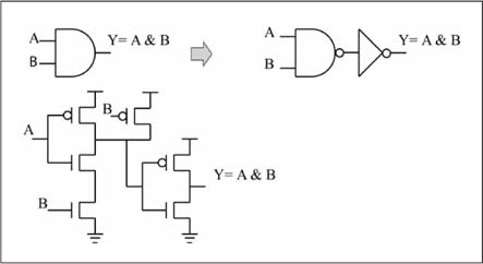
Figure 1.13 shows that a CMOS AND gate is actually built from a NAND gate followed by an inverter. Similarly, a CMOS OR gate is built from a NOR gate followed by an inverter. This clearly shows why replacing AND/OR logic with NAND gates via DeMorgan’s Law is a good idea. The resulting circuit requires fewer transistors, meaning it is faster, consumes less power, and is cheaper to manufacture!
Combinational Building Blocks
Building logic circuits on a gate-by-gate basis is an exercise that can be quite fun, once. After that, you should look for shortcuts that reduce design time for complex circuits. One method for building complex combinational circuits quickly is to use combinational building blocks. The following sections describe some commonly used combinational building blocks; this list is by no means exhaustive. It should not be surprising that some of these building blocks (the adder and shifter) implement the arithmetic operations discussed earlier.
The Multiplexer
A K-to-1 multiplexer (or mux) steers one of K inputs to the output. The most common mux type is a 2-to-1 mux (two inputs, one output). A select control input S chooses the input that is passed to the output. The operation of 2-to-1 mux is written in C code as:
if (S) Y = A; else Y = B;
This C code description of a mux reads as “if S is non-zero, output Y is equal to A, otherwise output Y is equal to B.” The Boolean equation for a 1-bit 2-to-1 mux is given in Equation 1.2.
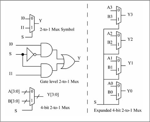
Figure 1.14 shows the gate equivalent for a 1-bit 2-to-1 mux and how a 4-bit 2-to-1 mux is built from four of these 1-bit building blocks. The 4-bit mux symbol in Figure 1.14 uses a bus labeling notation for the A and B inputs. In this context, a bus is simply a collection of parallel wires; a bus named A with N wires is designated as A[N–1:0]. The LSb and MSb of bus A are A[0] and A[N–1], respectively. If N = 8, the entire bus A is labeled as A[7:0], the LSb is A[0], and the MSb is A[7].
Figure 1.14
One-bit 2-to-1 mux, 4-bit 2-to-1 mux
The Adder
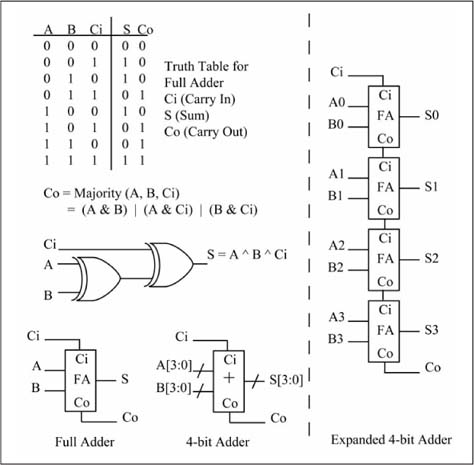
The adder takes two n-bit inputs (A, B) and computes the n-bit sum (A + B). Most adders have a carry-in bit input for the LSb addition and a carry-out bit output from the MSb addition. A full adder logic circuit that adds A + B + Ci (carry-in) and produces the sum (S) and carry-out (Co) is a 1-bit building block of most adder circuits. Figure 1.15 shows the truth table, Boolean equations, and logic network for a full adder. The same figure shows how to build a 4-bit ripple-carry adder from four 1-bit full adders; the term ripple-carry is used because the carry ripples from the least significant bit to the most significant bit. There are many other ways to build an adder; this is the simplest form of a binary adder.
Figure 1.15
One-bit adder, 4-bit ripple adder
The Incrementer
The operation of an incrementer is described by the following C code:
if (INC) Y = A + 1; else Y = A;
The INC (increment) input is a single bit input that determines if the n-bit output is A + 1 or just A. An incrementer can be built from an adder by connecting all bits of one n-bit input to zero and using the carry-in input as the INC input. This computes the sum Y = A + 0 + 1 when INC = 1 or the value Y = A + 0 + 0 when INC = 0. There are more efficient methods in terms of logic gate count to implement an incrementer, but this illustrates the flexibility of combinational building blocks in implementing different functions.
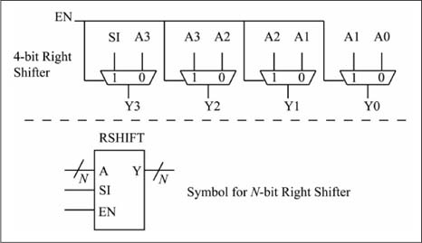
The Shifter
There are many varieties of shifter combinational building blocks. The simplest type shifts by only one position and in a fixed direction (either left or right). More complex types can shift multiple positions (a barrel shifter) in either direction. Figure 1.16 shows the logic symbol for an n-bit right shifter and the internal details of a 4-bit right shifter. When EN = 1, then Y = A >> 1 with the SI input providing the input bit for the MSb. When EN = 0, then Y = A, and the SI input has no effect. This is another example of simple combinational building blocks (2-to-1 muxes) being used to build a more complex combinational building block.
Figure 1.16
N-bit right shift symbol and 4-bit right shift details
Memory
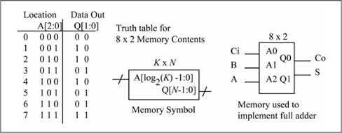
A K x N memory device has K locations, with each location containing n bits. Thus, a 16 x 1 memory has 16 locations, with each location containing 1 bit. The address inputs specify the location whose contents appear on the data output. Because the address bits uniquely specify 1 of K locations, the minimum width of the address bus is ceil(log2 K). The output data bus has n bits as it is used to output a memory location’s content. Following these rules, a 16 x 1 memory has ceil(log2 16) = 4 address inputs and one data output. The idealistic view of memory presented here assumes a memory type with only these inputs and outputs, with memory contents loaded by some external means not discussed here. The most common usage of memory is to store data, and thus it’s actually a sequential logic element, which is defined in the next section. However, a memory device can also be used to implement combinational logic functions, and so that usage scenario is discussed here.
Figure 1.17 shows an 8 x 2 memory used to implement the sum and carry-out equations of the full adder. The full adder inputs are connected to the 3-bit address bus as A = ADDR2, B = ADDR1, and Ci = ADDR0. The 2-bit data output bus provides the outputs as Co = Q0 and S = Q1. When a memory is used in this way, it known as a lookup table (LUT). Changing the memory contents changes the logic function(s) implemented by the memory. Thus, a memory can be thought of as a programmable logic gate. Field programmable gate arrays (FPGAs) have thousands or even millions of small memories in one integrated circuit that can be programmed by the user for implementing logic functions.
Sample Question: How many address and data lines does a 4 Ki x 16 memory have?
Answer: The number of address inputs is ceil(log2 4Ki) = ceil(log2 22 * 210) = ceil(log2 212) = 12. The number of data outputs is 16.
Figure 1.17
Full adder implemented by an 8 x 2 memory
Understanding Sequential Logic
The output of a combinational logic block is always uniquely defined by its current inputs. In contrast, the output of a sequential logic element is defined by its current inputs and also its current state, a value that is internal to the sequential logic element. A sequential logic element is a form of a memory device in that it retains internal state information between operations. In discussing sequential logic, the terms asserted and negated are used in reference to inputs, in addition to the previously defined terms of high-true and low-true. A high-true input has a high voltage level for TRUE and a low voltage level for FALSE. A low-true input has a low voltage level for TRUE and a high voltage level for FALSE. When an input is asserted, it is said to contain a TRUE value; a negated input contains a FALSE value. The symbol for a sequential logic element uses a bubble on an input to indicate low-true input or output.
The Clock Signal
An important signal in a sequential logic circuit is the clock signal, whose waveform and associated definitions are shown in Figure 1.18. The following definitions are used in reference to clock waveforms:
![]() A rising edge is a transition from low to high; a falling edge is a transition from high to low.
A rising edge is a transition from low to high; a falling edge is a transition from high to low.
![]() The period of a clock is the time in seconds (s) between two edges of the same type. A clock waveform typically has a fixed period; in other words, the period does not vary over time.
The period of a clock is the time in seconds (s) between two edges of the same type. A clock waveform typically has a fixed period; in other words, the period does not vary over time.
![]() The frequency of a clock is defined as 1/(period) and is measured in Hertz (Hz), where 1 Hz = 1/(1 s) (a 1 Hz clock has a period of 1 second).
The frequency of a clock is defined as 1/(period) and is measured in Hertz (Hz), where 1 Hz = 1/(1 s) (a 1 Hz clock has a period of 1 second).
![]() The high pulse width (PWH) is the amount of time the clock is high between a rising and falling edge; the low pulse width (PWL) is the amount of time the clock remains low between a falling and rising edge. The duty cycle is the percentage of time that the clock remains high.
The high pulse width (PWH) is the amount of time the clock is high between a rising and falling edge; the low pulse width (PWL) is the amount of time the clock remains low between a falling and rising edge. The duty cycle is the percentage of time that the clock remains high.
Clock signal equations are summarized in Equations 1.3 through 1.7 as:
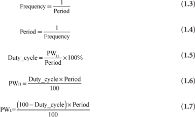
Figure 1.18, the clock waveform, is an example of a timing diagram, which is a method for describing time-dependent behavior of digital systems. In a timing diagram, one or more waveforms can be displayed, and time is assumed to increase from left to right. A waveform event is a change in waveform value. If waveform event A occurs to the right of waveform event B, then A occurs after B in time. Thus, there is an implied time ordering of events that flows left to right. The clock waveform shown in Figure 1.18 is an idealized view of a clock signal; an oscilloscope trace of an actual clock signal would reveal visible rise and fall times for clock edges, and perhaps ringing (small oscillations) on the end of rising and falling edges.
Figure 1.18
Clock signal definitions
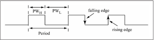
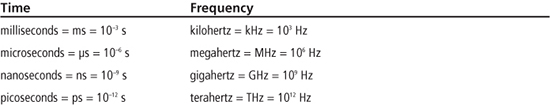
Table 1.4 lists commonly used units for time and frequency. A 1 kHz clock has a period of 1 ms, a 1 MHz clock has a period of 1 μs, and so forth. Timing and frequency specifications of digital circuits are contained in datasheets provided by the manufacturer. Time and frequency values are always specified using one of these units; in other words, a time is never specified as 1.05e–4 (shorthand for 1.05 × 10⁻⁴); instead, it is specified as 105 μs.
Table 1.4: Common Units for Time and Frequency
Sample Question: A clock has a duty cycle of 40 percent and a frequency of 19.2 kHz. What is the period and low pulse width, in microseconds?
Answer: The period is 1/(19.2 kHz) = 1/(19.2 × 103) = 5.21 × 10⁻⁵ s. To convert this value to microseconds, do a unit conversion via: (5.21 × 10⁻⁵ s) × (1 μs/1 × 10–6 s) = 52.1 μs.
PWL = ((100 – Duty_cycle) × Period)/100 = ((100 – 40) × 52.1 μs)/100 = 31.3 μs.
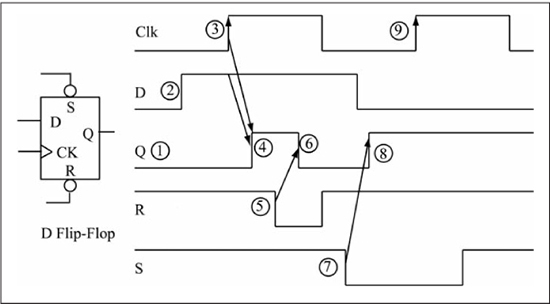
The D Flip-Flop
There are many varieties of sequential logic elements. This section reviews only the dominant type used in digital logic design, the D Flip-Flop (DFF).
A DFF, as seen in Figure 1.19, can have the following input signals:
![]() CK (input): The clock input; the arrival of the clock active edge sets the internal state of the DFF equal to the data input if the asynchronous inputs R, S are negated. The rising clock edge is the active clock edge for the DFF in Figure 1.19; it is said to be rising-edge triggered. A falling-edge triggered DFF has a bubble on its clock input.
CK (input): The clock input; the arrival of the clock active edge sets the internal state of the DFF equal to the data input if the asynchronous inputs R, S are negated. The rising clock edge is the active clock edge for the DFF in Figure 1.19; it is said to be rising-edge triggered. A falling-edge triggered DFF has a bubble on its clock input.
![]() D (input): The data input; the internal state of the DFF is set to this value on the arrival of an active clock edge if the asynchronous inputs R, S are negated. The D input is said to be a synchronous input as it can only affect the DFF on arrival of an active clock edge.
D (input): The data input; the internal state of the DFF is set to this value on the arrival of an active clock edge if the asynchronous inputs R, S are negated. The D input is said to be a synchronous input as it can only affect the DFF on arrival of an active clock edge.
![]() S (input): The set input; the internal state of the DFF becomes a 1 when this input is asserted. In Figure 1.19 this is a low-true input, so a low voltage on this input asserts set. This input is said to be asynchronous as its operation is independent of the clock input.
S (input): The set input; the internal state of the DFF becomes a 1 when this input is asserted. In Figure 1.19 this is a low-true input, so a low voltage on this input asserts set. This input is said to be asynchronous as its operation is independent of the clock input.
![]() R (input): The reset input; the internal state of the DFF becomes a 0 when this input is asserted. In Figure 1.19 this is a low-true input, so a low voltage on this input asserts reset. This input is also an asynchronous input.
R (input): The reset input; the internal state of the DFF becomes a 0 when this input is asserted. In Figure 1.19 this is a low-true input, so a low voltage on this input asserts reset. This input is also an asynchronous input.
![]() Q (output): The Q output is the value of the internal state bit.
Q (output): The Q output is the value of the internal state bit.
Not all DFFs have S and R inputs; all DFFs have at least CK, D, and Q. The timing diagram in Figure 1.19 contains the following sequence of events:
1. The initial value of the DFF state bit is 0 as reflected by the Q output.
2. The D input becomes a 1, but this has no effect on the Q output, as a rising clock edge has not occurred.
3. A rising clock edge arrives.
4. The Q output changes to a 1 as the D value of 1 is clocked into the DFF by the rising clock edge. The time delay between the rising clock edge and the Q output becoming a 1 is known as a propagation delay; changes cannot occur instantaneously in physical logic circuits. Propagation delay values are dependent on the transistor topology of a logic gate and have different values for different inputs and gate types. A propagation delay given in a datasheet is specified as a maximum time for a given operating condition (supply voltage, ambient temperature). Timing diagrams in this book show propagation delay where appropriate.
5. The R input becomes a 0, asserting this input.
6. The Q output becomes a 0 after a propagation delay; note that this occurs independently of the clock edge, as the R input is an asynchronous input.
7. The S input becomes a 0, asserting this input.
8. The Q output becomes a 1 after a propagation delay; again, this occurs independent of the clock edge, as the S input is an asynchronous input.
9. A rising clock edge arrives. The D input is a 0, but this value is not clocked into the DFF, as the S input is still asserted, which keeps the internal state at a 1.
The DFF is the most commonly used edge-triggered sequential logic element in digital logic, as it takes the fewest transistors to build. Other types of sequential logic elements include the JK Flip-Flop (JKFF) and T Flip-Flop (TFF); both of these can be built by placing logic gates around a DFF.
Figure 1.19
D flip-flop symbol and operation
Sequential Building Blocks
Sequential building blocks are built using combinational building blocks and sequential logic elements. The following sections review some common sequential building blocks.
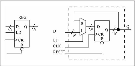
The Register
A register is used to store an n-bit value over successive clock periods. You might think that paralleling n DFFs would suffice, but the problem with a DFF is that it samples its D input on every active clock edge, potentially changing its value every active clock edge. Figure 1.20 shows an n-bit register built from an n-bit DFF and an n-bit 2-to-1 mux. When the load input (LD) is 1, the DFF D input receives the value of the external D input by way of the mux, and thus the register is loaded with a new value on the next active clock edge. When LD is 0, the DFF D input is connected to the DFF Q output; thus each active clock edge reloads the DFFs with their current output values.
In this way, the register retains its current value over multiple clock cycles when the load input is negated (LD = 0). Registers are key components of all computers, and Figure 1.20 should be the physical element envisioned when the term register is used in future chapters on microprocessor operation.
The Counter
A counter is a register that has the additional capability of being able to increment (count up) or decrement (count down), or both. Figure 1.21 shows an n-bit counter that can count up. An n-bit incrementer has been added to the register design of Figure 1.20 to provide the counter functionality. The counter counts up by one when INC = 1 and LD = 0 on a rising clock edge as the DFF D input sees the value Q + 1. When INC = 0 and LD = 1, the counter loads the external D input value on the active clock edge. This allows the counter to be initialized to a value other than zero. When INC = 0 and LD = 0, the counter holds its current value. Counters are useful for producing addresses used to access memories, as sequential access of memory content is a commonly needed operation in computer systems.
The Shift Register
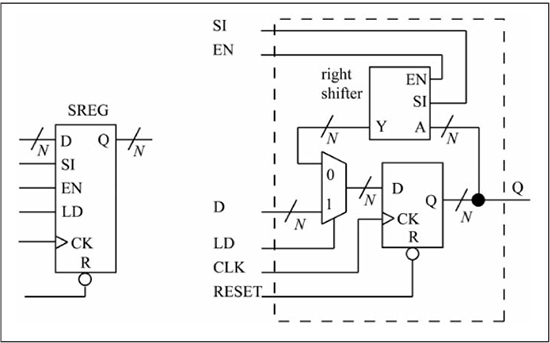
A shift register is a register that has the additional capability of being able to shift left, right, or both directions. Figure 1.22 shows a shift register that can shift right by 1 when SHIFT = 1 and LD = 0. It uses the same design as the counter, except that a shift-right block has replaced the incrementer block. Shift registers are useful in computer input/output where an n-bit value must be communicated serially (bit by bit) to another device. The concept of serial input/output is covered in greater detail in Chapter 10.
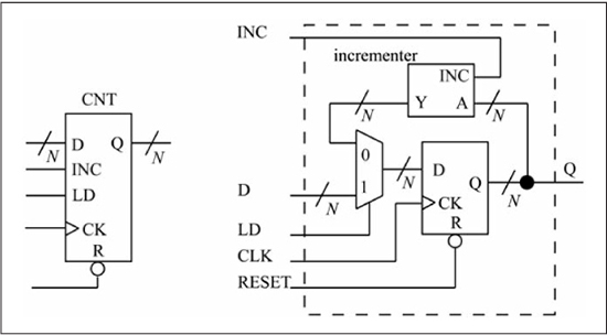
Figure 1.22
N-bit shift register
At this point, the usefulness of the concept of combinational and sequential building blocks should be apparent. You can envision other useful combinational building blocks such as a subtractor, decrementer, adder/subtractor, and other sequential building blocks such as up/down counters, or combined counter/shift registers. These components form the basis for the logic circuits used within modern computers.
Encoding Character Data
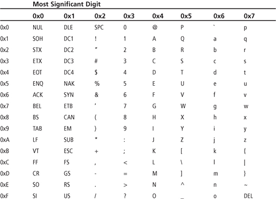
Up to this point, the data encodings discussed have been for numerical representation of unsigned integers. Another common data type manipulated by computer systems is text, such as that printed on this page. The American Standard Code for Information Interchange (ASCII) is a 7-bit code used for encoding the English alphabet. The ASCII code contains uppercase letters, lowercase letters, punctuation marks, numerals, printer control codes, and special symbols. Table 1.5 shows the ASCII code; the top row specifies the most significant hex digit and the leftmost column the least significant hex digit of the 7-bit hex code. Thus, an A has the code 0x41, a 4 is 0x34, a z is 0x7A, and so on. The codes that are less than 0x20 are nonprintable characters that have various uses; some are printer control codes such as 0x0D (carriage return) and 0x0A (line feed). Eight bits are normally used to encode an ASCII character, with the eighth bit cleared to zero.
With the advent of the Web and the necessity to exchange binary-encoded text in other languages, the universal character-encoding standard, Unicode, was created (see www.unicode.org for more information). The Unicode goal is to provide a unique encoding for every character, numeral, punctuation mark, and so forth, contained within every known language. The Unicode standard allows 8-bit (1 byte), 16-bit (2 byte), and 32-bit (4 byte) encodings. The 8-bit and 16-bit encodings are subsets of the 32-bit encodings; the first 128 codes (0x00 to 0x7F) are the same as the ASCII code for compatibility. Using 32 bits for each character allows for 4,294,967,296 unique characters, which is sufficient for the known character sets of the world. Individual character sets (Latin, Greek, Chinese, and so on) are assigned ranges within Unicode. Portions of the code are also reserved for use by private applications, so these codes are not assigned to any language. This book uses ASCII exclusively for character data encoding, but be aware that more sophisticated methods for text encoding exist. The number of different items in the computer world that have binary encodings is large, and thus you must be told what is being encoded in order to decipher a binary code. For example, the binary value 0b01000001 (0x41) can represent either the ASCII code for an “A” (uppercase A), or the number 65 (4 * 16 + 1 = 65), or something else entirely. Throughout this book’s remaining chapters, you will learn about other types of binary codes and the items that they encode.
Sample Question: What character string is represented by “0x48 0x65 0x6C 0x6C 0x6F 0x20 0x57 0x6F 0x72 0x6C 0x64 0x21”?
Answer: Translating character by character yields the popular test message: “Hello World!” Note that the string contains a space character (0x20) and an exclamation mark “!” (0x21).
Summary
The goal of this chapter was to refresh some topics you have encountered previously concerning number systems, binary encoding, Boolean algebra, logic gates, combinational building blocks, and sequential building blocks. The next chapter uses these building blocks to introduce the concept of a stored program machine as a means of implementing a digital system.
Review Problems
The answers to the odd-numbered problems can be found in Appendix C.
1. How many bits does it take to represent 40 items?
2. What is the largest unsigned integer that can be represented in 7 bits?
3. Convert the value 120 to binary using 8 bits.
4. Convert 89 to hex using 8 bits.
5. Convert 0xF4 to binary.
6. Convert 0xF4 to decimal.
7. Convert the value 0b10110111 to decimal.
8. Compute 0xB2 + 0x9F and give the result in hex.
9. Compute 0xB2 – 0x9F and give the result in hex. Check your work by verifying that 0xB2 + ~(0x9F) + 0x1 produces the same result. To compute ~(0x9F), complement each bit.
10. Draw the logic network and derive the truth table for the logic function F = (A&B) | C.
11. Derive the CMOS transistor network that implements the NOR function.
12. Compute 0xC3 >> 2; give the value in hex (this is a right shift by two).
13. Compute 0x2A << 1; give the value in hex (this is a left shift by one).
14. What is the period of a 400 kHz clock in microseconds?
15. Given a 30 percent duty cycle clock with a high pulse width of 20 μs, what is the clock frequency in kHz?
16. Design an n-bit subtractor using an adder with a carry-in input and the fact that A – B = A + ~B + 1.
17. Design an n-bit adder/subtractor that has an external input called SUB that when 1, performs a subtraction, when 0, performs an addition. (Hint: Use an adder with a carry-in input and a mux.)
18. Design a left-shift by one combinational building block.
19. Design a counter that can count either up or down. Assume that you have incrementer and decrementer building blocks available.
20. Write your first name as 8-bit hex values using ASCII encoding.