
CHAPTER 11
DATA CONVERSION
This chapter discusses a few of the many analog-to-digital converter (ADC) and digital-to-analog converter (DAC) architectures, and the advantages and disadvantages of each. The successive approximation ADC in the PIC24 family and an external serial DAC are covered and example applications are explained.
Learning Objectives
After reading this chapter, you will be able to:
![]() Describe the differences between sampling and quantization and the differences among ADCs, DACs, and sample-and-hold amplifiers (SHAs).
Describe the differences between sampling and quantization and the differences among ADCs, DACs, and sample-and-hold amplifiers (SHAs).
![]() Describe the operation of a successive-approximation ADC.
Describe the operation of a successive-approximation ADC.
![]() Implement a simple single-channel data acquisition system using the dsPIC33EP128GP502 analog- to-digital converter peripheral.
Implement a simple single-channel data acquisition system using the dsPIC33EP128GP502 analog- to-digital converter peripheral.
![]() Construct a parallel R-2R resistor ladder flash DAC using processors in the PIC24 family.
Construct a parallel R-2R resistor ladder flash DAC using processors in the PIC24 family.
![]() Control an external DAC from a dsPIC33EP128GP502 device using the SPI interface.
Control an external DAC from a dsPIC33EP128GP502 device using the SPI interface.
![]() Construct a simple sinusoid function waveform generator with the dsPIC33EP128GP502 and an external DAC.
Construct a simple sinusoid function waveform generator with the dsPIC33EP128GP502 and an external DAC.
Data Conversion Basics
As predicted by Moore’s Law in 1964 [1], digital computing power has exponentially increased at ever smaller, incremental costs. For example, as you’ve seen in the previous chapters, processors in the PIC24 family have the capability to replace several discrete integrated circuit chips. With this increase of computing power, many applications usually accomplished with analog circuitry are now implemented with digital electronics. However, the real world still is and will always be a fundamentally analog place. To bring the digital processing of the PIC24 family and its benefits to bear on real-world applications, the analog signal of interest must be translated into a format the PIC24 μC can understand. This translation is performed by the combination of a sensor and an analog-to-digital converter (ADC), as shown in Figure 11.1. The purpose of the sensor is to convert the desired real-world physical quantity (e.g., temperature, humidity, force, displacement, or acceleration) into a form—voltage, current, or resistance—that is more compatible with electronics. For purposes of this discussion, you can assume the desired electronic representation for signals are always voltages. Therefore, the sensor in Figure 11.1 converts the desired real-world analog quantity, w(t), into a voltage, x(t), which represents the same information. Then, the ADC converts the voltage representation, x(t), of the desired information into a digital number, x[k], for use by the microprocessor, where k is an index into a sequence of digital numbers. After processing by the PIC24 μC, the resulting digital stream of information, y[k], must be returned to an analog electronic form by a digital-to-analog converter (DAC). The output of the DAC is typically a voltage, but can be a current or other electronic representation. Then, the electronic voltage form, y(t), of the microprocessor output can be converted into the desired real-world physical quantity, z(t), by the transducer. Transducer outputs can be nearly anything, including linear or rotational motion, temperature, resistance, hydraulic fluid pressure change, acoustical sound, light intensity, light color, and so on. The transducer output information is “consumed” by the analog world—changing the world in which the microprocessor operates or absorbed by human senses, often sight or hearing. Of course, this process repeats over and over again as the microprocessor continues to sense and react to the world in which it is placed. An illustration of this cyclic information flow is shown in Figure 11.1.
ADCs and DACs are ubiquitous in computing systems. Many electronic products—including compact disc and MP3 players, camcorders, digital cellular phones, computer sound cards, computer graphics adapters, and high-definition televisions—contain one or more data converters. Because ADCs are so useful and required by so many small microprocessor applications, microprocessor architects often include an ADC as a built-in peripheral. The Microchip PIC24 μC designers did just that.
Sensors and Transducers
A comprehensive study of the types and construction of sensors and transducers represented by boxes in Figure 11.1 is a vast undertaking. This text introduces only the most basic concepts of sensors and transducers, and includes a couple of examples to illustrate the way in which an embedded microcomputer system designer might use them.
Figure 11.1
Typical use of a PIC24 family member to interface with the “analog” world

Transducers are devices that convert energy from one form to another. By this definition, the sensor in Figure 11.1 is also a transducer, because it converts the energy in the desired physical quantity w(t) into electrical energy in the form of a voltage x(t). In practice, if a transducer is used to convert some physical value into a more readily observable form, typically an electronic form, the transducer is called a sensor.
For a sensor to be most useful, the relationship between the physical quantity w(t) and the sensor voltage output x(t) must be accurately defined and stable. For ease of use, it is most desirable that the sensor have a linear mapping between w(t) and x(t). Consider a fictitious humidity sensor that creates a voltage of 0-2 V proportional to the percent relative humidity (%RH) of its environment. In this case, the sensor input w(t) represents the %RH, while the sensor output x(t) is the voltage between zero and two volts linearly related to %RH. The proportionality constant that relates the sensor input to its output is found by dividing the sensor’s output range by the sensor’s input range:
2 V / 100%RH = 1/50 V/%RH = 20 mV/%RH
Sample Question: If the relative humidity w(t) is 22%, what is the generated output voltage x(t) for this fictitious humidity sensor?
Answer: The proportionality constant for the humidity sensor is 20 mV/%RH. If the relative humidity w(t) is 22%, you could expect the sensor to generate an output voltage x(t) = (22%RH) (20 mV/%RH) = 440 mV = 0.44 V.
Digital computers operate with positive voltages. The purely linear relationship for the humidity sensor would not be compatible with a digital computer if the sensed physical quantity can take on negative values. Consider another fictitious sensor that measures the terrestrial elevation in meters above mean seal level (MSL). This sensor must be capable of measuring the elevation of the earth’s extremes: the shores of the Dead Sea (–424 m) and the peak of Mount Everest (8,848 m).
The elevation sensor measures the terrestrial elevation w(t) in meters and generates a voltage x(t) that varies 0.15 mV per meter elevation with a bias of 0.5 V. That is, the sensor output voltage x(t) (in mV) is given by
x(t) = 0.15 * w(t) + 500
where w(t) is the terrestrial elevation in meters and noting that 0.5 V=500 mV. It is easily seen that the terrestrial elevation sensor produces a positive voltage output for any terrestrial elevation on earth. The sensor’s voltage output x(t) at the Dead Sea shore is 0.15 mV/m * (–424 m) + 500 mV = 436 mV = 0.436 V, and the sensor’s voltage output atop Mount Everest is 0.15 mV/m * (8848 m) + 500 mV = 1827 mV = 1.827 V.
Sample Question: What is the voltage output x(t) of the fictitious terrestrial elevation sensor at the elevation extremes of the United States—Bad Water Basin, Death Valley, CA at –86 m and the peak of Denali (Mt. McKinley), Alaska at 6,168 m?
Answer: The proportionality constant for the terrestrial elevation sensor is 0.15 mV/m with a bias of 500 mV. At Bad Water Basin, the elevation w(t) is –86 m, so you would expect the sensor to generate an output voltage x(t) = (–86 m) (0.15 mV/m) + 500 mV = 487 mV = 0.487 V. At Denali, the elevation w(t) is 6,186 m, so you would expect the sensor to generate an output voltage x(t) = (6186 m) (0.15 mV/m) + 500 mV = 1428 mV = 1.428 V.
Of course, the purpose of the sensor is to observe the physical quantity so the reverse relationship is typically how sensor data is processed. The microprocessor and its user senses or observes the sensor output x(t) and desires to know the sensor input. For this example, user observes the voltage x(t) and wants to know the relative humidity sensed by the sensor.
Sample Question: The example humidity sensor generates an output voltage x(t) = 1.47 V. What is the relative humidity of the environment in which the sensor has been placed?
Answer: The proportionality constant for the humidity sensor is 20 mV/%RH. If the sensor output voltage is 1.47 V, the sensor is placed in the analog world environment where the relative humidity is %RH = 1.47 V / (0.02 V/%RH) = 73.5%RH.
Sample Question: The example terrestrial elevation sensor generates an output voltage x(t) = 0.741 V. What is the elevation (in meters) where the sensor has been placed?
Answer: The proportionality constant for the humidity sensor is 0.15 mV/m with a bias of 500 mV. If the sensor output voltage is 0.741 V, the sensor is placed in the analog world at an elevation w(t) = (741 mV – 500 mV) / (0.15 mV/m) = 1607 m above MSL.
The only real difference between the sensor and the transducer in Figure 11.1 is the direction of data movement. The concepts of the sensor and the humidity sensor example apply directly. Consider a transducer that is used to display the %RH on an instrument gauge. The instrument gauge is the transducer as it accepts an electronic signal y(t)—a voltage—and converts this energy into a visual form z(t)—the movement of a needle on an instrument. If your instrument accepts voltages 0-1 V to represent a display of 0-100%RH, it is readily seen that the desired transducer input y(t) to accurately display the 22%RH and 73.5%RH of these examples will be 0.22 V and 0.735 V, respectively.
Analog-to-Digital Conversion
From a programmer’s viewpoint, the ADCs and DACs in Figure 11.1 can be regarded as black boxes. That is, an ADC accepts an input of some analog quantity x(t), typically voltage, and provides an n-bit digital code x[k] as its output fs times per second that represents that analog input. The number fs is said to be the ADC’s sampling frequency. The black box DAC accepts an n-bit digital word y[k] as its input fs times per second and generates an equivalent analog output y(t), where y(t) is typically a voltage. The number fs is the DAC’s sampling frequency. For many purposes, this is a sufficient interpretation of data converters. However, knowledge of how the data conversion is done will help you understand why there are limitations on ADC and DAC operation, and should help you in configuring your data converter for the application at hand.
The methods by which a digital code is generated within an ADC are diverse. A detailed discussion would fill several books (a couple of references [66-67] on ADCs have been provided in Appendix D). The most common ADCs convert an analog voltage into a digital number. The digital number that an ADC generates can be in any encoding system, but is most typically represented in unsigned or signed binary.
ADCs and their capabilities are described by a bewildering number of parameters. A full discussion of ADC parameters is more appropriate with an advanced electronics background, and you are encouraged to explore the data conversion references in Appendix D. However, some basic descriptive parameters for ADCs must be understood to select and use them properly.
The speed of an ADC is measured as the minimum sampling period tmin, which specifies the shortest period of time required to convert an input voltage to a digital number. Minimum sampling period is equivalently reported as the maximum sampling frequency, the maximum number of samples that the ADC can convert in one second. The maximum sampling frequency fmax is found by fmax = 1/tmin. Of course, a faster ADC gives you a more accurate temporal picture of what the analog voltage input is doing, but this knowledge requires that your microprocessor must operate on and/or store more data.
An ADC’s resolution is the smallest change in its analog input that is detectable at its output, usually a change of ±1 in the ADC’s digital output. In other words, resolution represents the change in ADC’s analog input that corresponds to a 1 LSb change in output. ADC precision is the number of levels that the ADC can distinguish. Sometimes, ADC precision is quoted by the number of binary bits required to encode the number of levels. The ADC range is the total span over which inputs can be converted accurately. Quite often, the range extremes, VREF+ and VREF – in the case of voltage conversion, are provided as ADC inputs.
Sample Question: How many bits of precision would an ADC require to distinguish 1 μV (1 μV = 1 • 10–6 V) differences over a range 0–2 V?
Answer: There are 2 million (2 • 106 = 2 V/I μV) steps in a 0–2 V range. An ADC would need 21 bits of output (221 = 2,097,152) to encode these required 2,000,000 steps.
Sample Question: What is the range and resolution of an 8-bit ADC with VREF+ = 10 V and VREF– = –10 V?
Answer: The ADC’s range is 10 V – (–10 V) = 20 V. The resolution of the ADC is its range divided by its number of steps; therefore, the resolution of the ADC is 20 V/256 = 78.125 mV.
Sample Question: What is the maximum sampling frequency for the 8-bit ADC in the preceding question if the minimum sampling period is 2.5 μs?
Answer: The maximum sampling frequency fmax = 1 / tmin, so the ADC’s maximum sampling frequency is fmax = 1 / 2.5 μs = 400,000 Hz = 400 kHz.
Sample Question: If the ADC from the previous example is operating at maximum speed, how much storage is required to store one second of ADC output? One year’s worth?
Answer: Each ADC output is 1 byte. Therefore, one second of ADC output would occupy (400 kHz)(1 byte) = 400 KB. There are 107 seconds in one year. Thus, one year’s worth of data from the 8-bit ADC operating at maximum sampling frequency would be 400 KB/sec x 3.1536 x 10⁷ sec = 1.26144 x 1013 bytes, or a little more than 11 TiB. Thus, you would need more than 25 hard disk drives, each with 500 GB of capacity, to store a year’s worth of data from the ADC. That is a lot of storage space!
Most ADCs have uniform step sizes, which is the difference between the minimum and maximum voltages that correspond to the same output code. If step size is uniform or constant over the ADC range, the step size is equal to the resolution. (There are some specialty ADCs with non-uniform step sizes; for example, some audio ADCs have step sizes that change logarithmically over their range to match the response of the human ear.) Using the black box view of ADCs, an n-bit ADC with uniform step sizes divides its range into 2n equal segments. The ADC output is simply the number of the segment in which the ADC input lies.
Mathematically, the ADC digital output x[k] at sample time k is given in Equation 11.1.
In Equation 11.1, T is the ADC sampling period, x(kT) is the input voltage Vin at time kT, k is a numerical index that represents time, and Qn{} is a function that converts its argument to an integer that can be represented by n bits. The Qn{} operation is typically performed by truncation or rounding. Because information is lost due to rounding or truncation in Qn{}, analog-to-digital conversion always introduces some error. The difference between the actual ADC input value and the value implied by the ADC’s digital output is called quantization error, which can be made smaller by increasing the ADC’s precision.
Sample Question: Assuming the 8-bit ADC in the prior examples performs conversion by rounding, what is the ADC output code for –7.35 V? 2.0 V? Do your answers change if the conversion is done by truncation?
Answer: The example 8-bit ADC compares its input voltage Vin against the 256 equally spaced reference voltages between –10 V and +10 V. The size of these equal spaces is the step size, which is 78.125 mV. The k-th reference voltage of these 256 voltages is found by Vrefk = –10 + 0.078125 k V.
Examining the set of 256 reference voltages, you can easily determine that the reference voltages with k = 34 is –7.34375 V and k = 35 is –7.2656 V. Comparing the –7.35 V input voltage with the set of 256 reference voltages, you determine that the k = 34 reference voltage is the closest value to –7.35 V and would be selected if the conversion were done by rounding. The ADC output for –7.35 V would be 34, or 0x22.
Repeating the preceding process, you’ll find the voltages 1.953125 V corresponding to k = 153, and 2.03125 V corresponding to k = 154. The closest value to +2.0 V is 2.03125 V. Therefore, the ADC result for +2.0 V would be 154, or 0x9A.
Truncation is the operation of always rounding toward zero. If the ADC were to truncate rather than round, the answer for the first voltage would change. The ADC result for –7.35 V would be 35, or 0x23, and the result for +2.0 V would be 154, or 0x9A.
Sample Question: Assuming that the humidity sensor in the previous section is being sampled by an 8-bit ADC with VREF+ = 3.3 V and VREF– = 0 V, what ADC digital output code is created when the relative humidity is 22% and 73.5%? Assume the ADC performs rounding in its quantization.
Answer: The ADC range is 3.3 V and the ADC has 28 = 256 steps, or output codes. The ADC input voltage for 22%RH is 440 mV. Therefore, the 8-bit ADC output code for 22%RH is
floor ((0.44 V)(256 steps) / (3.3 V) ) = floor( 34.1 ) = 34 = 0x22
For the 73.5%RH case, the 8-bit ADC output code is
floor ( (1.47 V)(256 steps) / (3.3 V) ) = floor( 144.03 ) = 114 = 0x72
Sample Question: The fictitious humidity sensor of the previous section is sampled by a 12-bit ADC with VREF+ = 3.0 V and VREF– = 0 V. What is the %RH if the ADC has a digital output code of 0x1AB?
Answer: Using a 12-bit ADC with VREF+ = 3.0 V and VREF– = 0 V, the digital code of 0x1AB corresponds to an ADC input voltage x(t) of
x(t) = (0x1AB / 212) (3.0 V) = (427 / 4096) (3.0V) = 312.7 mV
Using the sensor’s constant of 20 mV/%RH, the relative humidity is 312.7 mV / (20 mV/%RH) = 15.6%RH—a very dry day.
Sample Question: The fictitious terrestrial elevation sensor of the previous section is sampled by a 12-bit ADC with VREF+ = 2.0 V and VREF– = 0 V. What is the sensor’s elevation if the ADC has digital output code of 0x466?
Answer: Using a 12-bit ADC with VREF+ = 2.0 V and VREF– = 0 V, the digital code of 0x466 corresponds to an ADC input voltage x(t) of
x(t) = (0x466 / 212) (2.0 V) = (1126 / 4096) (2.0V) = 550 mV
Using the sensor’s equation x(t) = 0.15 * w(t) + 500, the sensor’s elevation is (550 mV – 500 mV) / 0.15 mV/m = 333 m.
The basic building block in nearly all ADCs is the voltage comparator. Figure 11.2 shows a voltage comparator circuit symbol. The circuitry inside a comparator can be quite complex, so consider the comparator in Figure 11.2 as a black box.
Figure 11.2
Voltage comparator circuit symbol and operation

If the positive input terminal voltage V+ is greater than the negative input terminal voltage V–, the comparator output is the comparator’s positive power supply voltage Vp. If V+ is less than V–, the comparator’s output is the negative supply voltage Vm. Therefore, you see that if Vp = VDD and Vm = 0, the comparator in Figure 11.2 will generate a digital signal that can communicate with digital logic, such as microprocessors. Because of this behavior, the voltage comparator is sometimes called a 1-bit ADC. By varying the comparator’s input voltages V+ and V– and using numerous comparators in different ways, an analog voltage can be compared to reference voltages and a digital number representation formed. There are many algorithms, circuits, and configurations by which this can be done. This section introduces a common voltage-mode ADC architecture used in many microcontrollers today: the successive approximation ADC.
Successive Approximation ADC
The successive approximation ADC converts the analog voltage present on its input to a numerical digital output code via a binary search. Consider the block diagram of an n-bit successive approximation ADC given in Figure 11.3. At the sample time, the ADC sets the MSb in the successive approximation register (SAR) to 1. All the remaining lower bits are reset to 0. This digital “guess” is converted back to an analog value and is compared with the input.
Figure 11.3
Successive approximation ADC

Therefore, the SAR contains a digital code representative of mid-scale (0b100...0). The DAC produces a corresponding mid-scale analog output, which is halfway between the minimum (VREF–) and maximum voltage (VREF+) that could be presented at the ADC input. If the input is at a higher potential than the feedback analog representation of the “guess” (Vin > VDAC), the MSb is left set to 1. If the input is at a lower potential than the feedback analog value, which is the case of Vin < VDAC, the MSb is reset to 0. In this step, the successive approximation ADC is determining the proper state of the MSb; in other words, whether the analog input value lies in the upper (MSb = 1) or lower (MSb = 0) half of the ADC’s range.
Now, the entire procedure is repeated for the second most significant bit. While the MSb is unchanged from the first approximation, the second MSb is set with the remaining lower bits reset. This digital code, an improved “guess,” is converted into an analog value (VDAC) and presented to the comparator. At this instant, the SAR value is either (0b1100...0) or (0b0100...0), depending on the outcome of the first approximation. If the analog input is at a higher potential than the feedback “guess” voltage, the second MSb is left at 1. If not, the second MSb is reset to 0. At the conclusion of this second approximation cycle, the two most significant bits in the register determine whether the ADC input is located in the highest (0b11), next-to-highest (0b10), next-to-lowest (0b01), or lowest (0b00) fourth of the ADC’s range.
Approximation cycles continue in this manner for each of the remaining lower order bits until all n bits have been examined. At the conclusion of each successive approximation cycle, the SAR digital code is converted back to an analog voltage and compared against the input voltage. In this way, each approximation halves the difference between the ADC’s input and the analog representation of the contents of the SAR. This is shown graphically in Figure 11.3.
Transmission of the digital code from the ADC at the conclusion of the successive approximation process may be done in two ways: serial or parallel. Each bit of the digital output code may be output from the ADC the instant it is computed. This particular flavor of successive approximation ADC is also known as the serial successive approximation ADC. The digital code in the SAR may be stored for parallel transmission upon completion of the sample conversion, or transmitted serially at a later time using some defined network protocol like I2C or SPI. When the time arises to convert the next sample, the contents of the SAR are reset and the entire procedure is repeated for the new analog voltage present on the input pin of the ADC.
A disadvantage of the successive approximation ADCs is the many internal operations that must occur for a single sample to be converted. In the n-bit converter, n approximations and comparisons must be performed in each sampling period. Therefore, an n-bit successive approximation ADC running at a sampling frequency of fs samples per second must run its internal circuit at a rate of nfs operations per second. The successive approximation ADC iteratively cuts the voltage range in half as it searches for the digital representation of the input voltage. As n grows, the circuitry of the successive approximation ADC becomes more problematic to design and function properly. The last few cycles of the successive approximation process are required to distinguish between two voltages very close in value. In practice, this is very difficult to do accurately.
Sample Question: Describe the conversion process for a 4-bit successive approximation ADC with VREF– = 0 V, VREF+ = 4 V, and Vin = 3.14159 V.
Answer: The ADC’s range is 4 V. The ADC resolution is 4 V/16 = 0.25 V. Therefore, each 1 LSb increase in output corresponds to an increase in 0.25 V of input. When the conversion process begins, the SAR is set to 0b1000 and the ADC input voltage Vin is compared with the midrange voltage 2.0 V (8/16 × 4 V). Since Vin > 2 V, the control logic leaves the MSb of the SAR set and sets the second MSb of the SAR. The SAR contents are now 0b1100, which represents the voltage 12/16 × 4 V, or 3.0 V. Because Vin > 3.0 V, the second MSb of the SAR is left set. The control logic sets the third MSb of the SAR, now 0b1110. The SAR contents cause the DAC to create a voltage of 14/16 × 4 V, or 3.5 V.
Because Vin < 3.5 V, the control logic clears the third MSb in the SAR and sets the SAR’s LSb. The SAR contents on the fourth cycle are 0b1101, which corresponds to a comparison voltage of 13/16 × 4, or 3.25 V. The comparator determines Vin < 3.25 V, so the LSb is cleared. The 4-bit digital result 0b1100 is computed in four cycles. Note that the final SAR digital code corresponds to an analog input voltage of 3.0 V, resulting in a quantization error of 3.14159 V – 3.0 V = 0.14159 V.
Sample and Hold Amplifiers
The preceding sections introduced you to a common ADC architecture, the successive approximation ADC; [66-67] discuss other architectures. The ADC is only half of the conversion process from an analog voltage to a digital number. In fact, the conversion step that the ADC performs is the last half of the process. The first half of the process is the sample and hold amplifier (SHA), which is introduced in this section.
In the successive approximation ADC architecture and in the dozens of alternative architectures detailed in other books, the ADC’s input voltage, Vin, must be perfectly stable or constant during the ADC conversion cycle. If the ADC input voltage Vin changes during the conversion step, the digital code value will likely be incorrect. The purpose of the SHA is to sample, or track, the voltage to be converted, and at the appropriate time, hold that voltage value constant while the ADC converts the voltage into the correct digital code. Figure 11.4 shows a circuit schematic symbol for an SHA along with an example waveform showing the SHA’s operation.
Figure 11.4
Sample and hold amplifier (SHA) operation
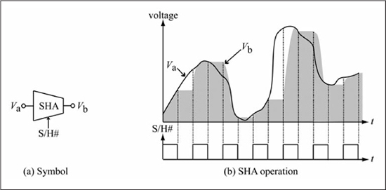
As seen in Figure 11.4, the SHA will sample its input voltage, Va (represented by the solid line) while its control signal S/H# = 1. During this “sampling” phase of operation, the SHA output, Vb (represented by the upper extent of the shaded area), will track the SHA input, i.e. Vb = Va. When the SHA’s control signal S/H# = 0, the SHA enters the “holding” phase of operation. While holding, the SHA output voltage, Vb, is held constant at the voltage value that Vb had at the time of the falling edge of S/H#. During the hold phase, the SHA input can change over a wide range of values, but Vb will remain constant. During several hold phases in Figure 11.4, you can see that the voltage Va continues to change while Vb stays constant. Obviously, when the SHA control signal changes to S/H# = 1 again, the SHA is expected to start tracking a voltage Va, which is dramatically different than the voltage that it was just holding. Under these conditions, the SHA will require a non-zero period of time for its output to start tracking accurately. This particular scenario is seen at several places in Figure 11.4. The amount of time required for the SHA output to accurately track the SHA input is a function of the SHA circuit design. If the SHA is ordered to “hold” before the tracking is accurate, the SHA output value, Vb, will be held constant at an erroneous voltage. If the SHA output is to represent accurately the SHA input, the SHA must be given adequate time to catch up with the SHA input voltage during the sample mode of operation.
The SHA can be viewed as an “analog transparent latch” during the sample phase and an “analog flip-flop” during the hold phase. The actual construction of the SHA circuit is as diverse as the circuits for ADCs. The interested reader is again directed to the references in Appendix D.
The usefulness of SHAs to the analog-to-digital conversion process should be readily apparent at this point. The voltage that you desire to convert to a digital code may be changing very rapidly, but the conversion process takes some amount of time. (The amount of time depends on your ADC architecture, of course.) Whatever ADC architecture you use, the ADC must have a constant voltage on which to operate. Therefore, nearly all practical analog-to-digital conversion integrated circuits contain an SHA circuit followed by an ADC circuit. The SHA samples the input voltage for a sufficient duration to insure that the SHA tracks the voltage perfectly. At this point, the SHA will hold the voltage for the time period required by subsequent ADC conversion to determine the correct digital code that represents the held voltage. When the ADC conversion is complete, the SHA is free to start sampling the input voltage again in preparation for the next conversion.
Now that you have examined the two main operations in converting a voltage to a digital code and three example ADC architectures, you will investigate the analog-to-digital converter peripheral in the Microchip dsPIC33EP128GP502 microcontroller.
The PIC24 Analog-to-Digital Converter
ADCs are used in so many small microprocessors and embedded systems that they are often included as a built-in peripheral. Microchip made just such a decision with their dsPIC33/PIC24 family of microprocessors. Each member of the dsPIC33/PIC24 microcontroller family includes a multiple-channel successive approximation ADC. The PIC24 microcontroller ADC peripheral can convert analog voltages into 10-bit or 12-bit digital codes. The word length of the ADC output is determined by the user. The number of available ADC input channels depends on the device and package chosen by the designer. For example, the PIC24HJ64GP206 and PIC24HJ256GP206 are available in 64-pin packages and provide 18 different input channels to their ADCs. The PIC24HJ64GP510 and PIC24HJ256GP610 are available in 100-pin packages and provide 32 different input channels to their ADCs. The PIC24HJ12GP202, dsPIC33EP128GP502, and PIC24HJ64GP202 devices are only available in 28-pin packages. With such a limited number of package pins, these devices only support ten different input channels to the internal ADC peripheral. Other PIC24 μC devices provide 6–32 input channels to the ADC. The required differences in using the PIC24 μC’s internal ADC between the different devices are usually minor and well documented in the datasheets. The remainder of this section focuses on the dsPIC33EP128GP502 device and the configuration and operation of its ADC.
Just like the other PIC24 μC peripherals (USART, interrupt, SPI) that were previously covered, the PIC24 μC’s internal ADC is controlled by a number of dedicated configuration, enable, and flag register bits. Since the ADC input connections are fundamentally analog values and must be treated differently than digital values, the external pins (ANx) that connect to the ADC are restricted to specific external pin locations. These ADC inputs cannot be remapped like many of the PIC24 μC’s digital peripherals. Different PIC24 μC devices have the same basic ADC operation; they only differ in the number of analog input channels available for conversion and the availability of direct memory access (DMA) support (discussed in Chapter 13). Figure 11.5 shows a simplified block diagram of the PIC24 ADC system. The dsPIC33EP128GP502 devices support analog input channels AN0-AN5 and provide direct memory access (DMA) support for ADC operations. For more information about using DMA with the PIC24 ADC, see on-line supplements available at www.reesemicro.com.
The PIC24 ADC peripheral is extremely flexible in its configuration. The features of the PIC24 ADC include (this list is not exhaustive):
![]() Convert voltage to 10-bit or 12-bit representations
Convert voltage to 10-bit or 12-bit representations
![]() Convert single-ended voltages—a voltage measured with respect to ground
Convert single-ended voltages—a voltage measured with respect to ground
![]() Convert differential voltages—a voltage difference between two arbitrary voltages
Convert differential voltages—a voltage difference between two arbitrary voltages
![]() Convert voltages on 1–32 ADC input channels
Convert voltages on 1–32 ADC input channels
![]() Sample ADC input channels sequentially, two channels simultaneously, or four channels simultaneously
Sample ADC input channels sequentially, two channels simultaneously, or four channels simultaneously
![]() Encode ADC output results as unsigned integer, signed integer, unsigned fractional, or signed fractional numbers
Encode ADC output results as unsigned integer, signed integer, unsigned fractional, or signed fractional numbers
![]() Use internal or external ADC reference voltages
Use internal or external ADC reference voltages
![]() Generate “ADC completion” interrupts every 1–16th sample
Generate “ADC completion” interrupts every 1–16th sample
![]() ADC operation timing and sequencing under user software control, automatic timing from internal ADC timer or one of the PIC24 timer peripherals
ADC operation timing and sequencing under user software control, automatic timing from internal ADC timer or one of the PIC24 timer peripherals
Figure 11.5
PIC24 analog-to-digital converter block diagram
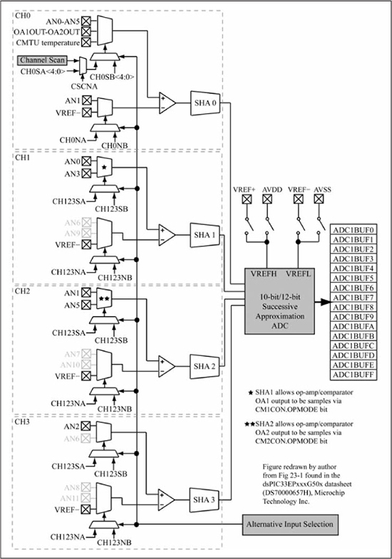
Source: Figure redrawn by author from Figure 23.1 found in the dsPIC33EPxxxG50x datasheet (DS70000657H), Microchip Technology Inc.
Some of the PIC24 ADC options just listed are mutually exclusive. However, most of the PIC24 ADC options are independent of the others. The number of combinations of PIC24 ADC configurations is enormous, and you can’t possibly examine each one. Therefore, this chapter focuses on using the PIC24 ADC in a configuration using only one sample channel with ADC operations being mostly automatic. Then, it presents a very brief description of each of the ADC configuration register bits for your further investigation.
In practice, the PIC24 ADC configuration you need is likely to be different from those presented here. You are encouraged to read and study the datasheets for your device carefully.
PIC24 ADC Configuration
The PIC24 ADC peripheral has several fundamental configuration options that drastically change the ADC operation. One of these fundamental options is whether the PIC24 ADC converts to a 10-bit or 12-bit result. Several other fundamental configuration options deal with the timing source and sequence of sample-and-hold and conversion operations. These options must be determined and set before you power up the PIC24 ADC module. If you attempt to change these fundamental configuration options when the ADC module is on, the ADC behavior is indeterminate.
The PIC24 ADC subsystem, like others found on the PIC24 μC, uses special function registers in two ways—either as data registers or as control registers. The ADC subsystem data registers are for transferring ADC result data from the successive approximation register to the user’s data memory. ADC control registers contain a mixture of configuration and status bits. Configuration bits specify the operating mode of the subsystem, while status bits indicate the operational state of the subsystem. Future implementations of the PIC24 μCs can have multiple ADCs with identical capabilities, so the ADC register names have a number (x) that designates its associated ADCx. For example, register ADxCON1 is one of the ADC control registers, and its name for ADC1 is AD1CON1. The code refers to named bits in ADC registers by their fully qualified structure reference (register.bitname) to make the functions portable to PIC24 microcontrollers with multiple ADCs, which do not have macros defined for individual ADC register bits. The dsPIC33EP128GP502 used in the reference system and all currently available members of the PIC24 family have only one ADC. Therefore, this section covers the PIC24 ADC subsystem using the first ADC, which is named AD1 or ADC1 in the datasheets.
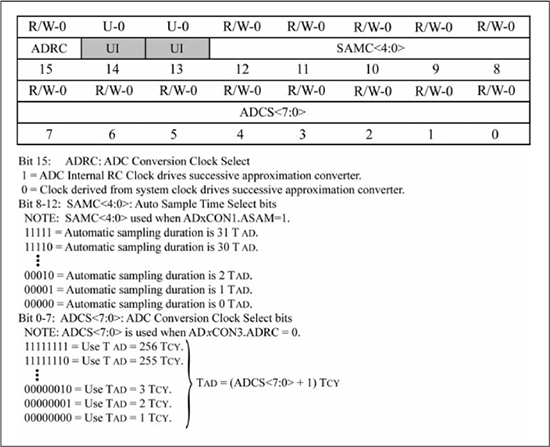
The ADC configuration example starts with 12-bit operation. Since this example chose a 12-bit result, only one of the four SHAs in the PIC24 ADC subsystems can be used due to a limitation of the PIC24 μC ADC. The four SHA channels are named CH0, CH1, CH2, and CH3. In the 12-bit mode, only channel CH0 can be used. If you were to select a 10-bit result, the ADC can “sample” one (CH0), two (CH0 and CH1), or four (CH0, CH1, CH2, and CH3) voltages simultaneously. To select 12-bit conversions, set AD1CON1.AD12B. Setting this bit results in a 12-bit successive approximation conversion process on the voltage being sampled and held by CH0. Figure 11.6 shows the location of the AD12B bit and the other bits in the AD1CON1 register.
Figure 11.6
The AD1CON1 configuration register

Source: Figure redrawn by author from Register 16.1 found in the dsPIC33E/PIC24E FRM ADC datasheet (DS70621C), Microchip Technology Inc.
The PIC24 ADC subsystem allows you, the programmer, to have a great deal of control over the conversion process. As you saw in the previous sections, the input voltage of interest must be sampled and held constant by the SHA. While the voltage is held, the successive approximation algorithm must clock through each bit of the result making the necessary comparisons. The PIC24 ADC allows the user to completely determine the timing of the sample, hold, and conversion steps. The PIC24 ADC also provides several semi-automatic and automatic configurations whereby the ADC subsystem proceeds from sample to hold to conversion steps. The progress of the ADC conversion cycle can be monitored by two bits: AD1CON1.SAMP and AD1CON1.DONE. The AD1CON1.SAMP bit is 1 when the SHAs are sampling and 0 when the SHAs are holding. The AD1CON1.DONE bit is 0 when the successive approximation conversion process is ongoing or not yet started and 1 when the conversion process is completed. The AD1CON1.DONE bit is automatically set by hardware when the conversion is completed and cleared by hardware when a new conversion starts.
The PIC24 ADC requires a clock source to control the timing between the sampling phase and the holding/converting phase. Furthermore, you learned earlier in this chapter that successive approximation ADCs require a clock to control the converter’s successive approximation control logic. The PIC24 ADC clock can be generated from the PIC24 instruction clock. This choice gives you great flexibility and control over the successive approximation timing. However, the instruction clock can easily generate a clock that is too fast for the PIC24 ADC. Therefore, the PIC24 ADC has its own internal RC oscillator to provide a timer to control the SHA operations and create the required clock cycles for the successive approximation algorithm. The ADC’s internal RC oscillator is a great choice since it is guaranteed to generate a clock signal adequate to work with the PIC24 ADC hardware. The internal ADC clock runs independently of the PIC24 instruction clock. Therefore, if you plan on performing any ADC operations during sleep mode, the internal ADC clock is your only choice. Example code will select the ADC’s internal RC clock by setting the AD1CON3.ADRC bit. Datasheets for the PIC24 μC indicate that the ADC internal RC clock generates a clock with a period TAD that is approximately equal to 250 ns. Figure 11.7 shows the location of the ADRC bit and of the other configuration bits in the AD1CON3 register.
Since this example configuration will have the ADC subsystem automatically progress from sample to hold to convert operations, you must instruct the PIC24 ADC how long to sample the voltage before switching to hold and then to convert. The time between the start of sampling and the start of conversion is determined by SAMC<4:0> in the AD1CON3 register. This five-bit number selects the sample time to be in the range of 0 to 31 TAD. The dsPIC33EP128GP502 ADC peripheral requires the sample time to be greater than 2 TAD in 10-bit ADC mode and greater than 3 TAD in 12-bit ADC mode. In this example, let’s be conservative and set AD1CON3.SAMC<4:0> = 31, or approximately 31 × 250 ns = 7.75 μs. This should be an adequate time for the PIC24 SHA to acquire an accurate copy of the ADC input voltage.
Figure 11.7
The AD1CON3 configuration register
Source: Figure redrawn by author from Register 16.3 found in the PIC24 FRM ADC datasheet (DS70621C), Microchip Technology Inc.
To instruct the ADC subsystem to automatically switch from sample mode to “hold and convert” mode based on this 31 TAD time interval, you must set the SSRC<2:0> bits in AD1CON1 equal to 7. The other values for AD1CON3.SSRC<2:0> allow software, an external interrupt, or general-purpose timers to determine the transition timing from sample to conversion. You will learn about these later in the chapter.
The successive approximation hardware must have negative and positive voltage references against which it can compare the voltage being held by the SHA. These two voltages were called VREF– and VREF+ in earlier discussions. The PIC24 ADC subsystem allows you to determine the source of these two voltages by the VCFG<2:0> bits in AD1CON2. In the example, setting AD1CON2.VCFG<2:0> to 0 will set the ADC’s VREF– = AVSS and VREF+ = AVDD. The voltages AVSS and AVDD are provided through dedicated pins on the PIC24 μC package. Figure 11.8 shows the location of the VCFG bits and the other configuration bits in the AD1CON2 register.
Figure 11.8
The AD1CON2 configuration register

Source: Figure redrawn by author from Register 16.2 found in the dsPIC33E/PIC24E FRM ADC datasheet (DS70621C), Microchip Technology Inc.
The ADC in the dsPIC33EP128GP502 can sample and convert up to six input channels. Other PIC24 μC models can convert between 6 and 32 input channels depending on the processor model and package. You must therefore select the desired input channel to provide an external voltage to the SHA in the ADC subsystem. Since you are performing a 12-bit ADC conversion, you must use CH0 in the ADC subsystem. The register AD1CHS0 selects the source of the voltages presented to the SHA in the CH0 path, as shown in Figure 11.5. If you want to apply the voltage on pin AN0 to your ADC, you need to set AD1CHS0.CH0SA<4:0> = 0x01, and clear the AD1CHS0.CH0NA bit in AD1CHS0. This will apply the voltage VAN0 on the AN0 pin to the positive input of the SHA and the voltage VREF– = AVSS to the negative input of the SHA. These settings in the AD1CHS0 register will configure the ADC to convert the “single-ended” voltage VAN0. The astute reader will see that setting the AD1CHS0.CH0NA bit will place the voltage VAN1 at the AN1 pin on the negative input of the SHA, thereby allowing for a “differential” conversion of the voltage, VAN0 –VAN1. The bits in the upper byte of the AD1CHS0 register are for an alternative setting mode that you will read about later in the chapter. Figure 11.9 shows the location of the ADRC bit and the other configuration bits in the AD1CHS0 register.
Figure 11.9
The AD1CHS0 configuration register
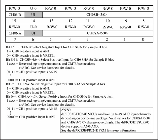
Source: Figure redrawn by author from Register 16.6 found in the dsPIC33E/PIC24E FRM ADC datasheet (DS70621C), Microchip Technology Inc.
It is extremely important to mention at this point that any ADC channel or ADC voltage reference that is enabled should have its corresponding port direction (TRISx) bit set. This configures the package pin to be an input. If this bit is cleared (output mode), the PIC24 ADC will attempt to use the driven pin voltage (VOL or VOH in the datasheet) as the ADC input or ADC voltage reference. This is seldom desired or useful. Furthermore, if the analog input voltage pin is a change notification (CNx) pin, the weak CN pull-up or pull-down resistors must be disabled by clearing the appropriate bit in the CNPUx register to avoid corrupting the sensitive analog voltage value. The macro CONFIG_Rxy_AS_ANALOG() performs these steps, where xy is the desired port and pin (e.g., CONFIG_RA0_AS_ANALOG()).
The AD1CON1.ASAM bit selects the condition that starts the sampling process. In the example case, initiation of the sampling process automatically proceeds, at a time 31 TAD later, to the conversion mode. The PIC24 successive approximation hardware requires 14 TAD to compute the 12-bit result and set the AD1CON1.DONE bit. Therefore, when you initiate the sampling operation by setting AD1CON1.SAMP, the ADC result will become available after the process runs its course.
Finally, after the PIC24 ADC subsystem has been fully configured to convert the voltage on the AN0 pin, you can turn on the ADC module. This is done by setting the AD1CON1.ADON bit. When AD1CON1.ADON = 1, the entire ADC module is enabled, powered up, and consuming power. When AD1CON1.ADON = 0, the ADC module is disabled and does not consume power. If the ADC module is not being used, the ADC should be turned off. In Figure 11.6, you see that the POR default value for AD1CON1.ADON is 0, which corresponds to the ADC peripheral being turned off by default after reset.
Figure 11.10 shows a function to perform the ADC configuration as just described. There are slight differences between the function in Figure 11.10 and the previous discussion. First, the function in Figure 11.10 begins by turning the AD1 module off. This step is required by the PIC24 μC datasheets, which specify that the ADC behavior is indeterminate if any of the timing, clock source, or auto-sampling bits are modified while the ADC is enabled. Secondly, the function in Figure 11.10 has an argument that is used to select the positive input voltage for CH0 (parameter u16_ch0PositiveMask, which is copied to the AD1CHS0.CHS0A<4:0> bits), which effectively determines the external pin that provides the voltage to convert. Useful #define macros for the AD1CHS0.CHS0A<4:0> bit values are provided in the includepic24_ports_mapping.h file. For example, the function in Figure 11.10 can be used to configure the AD1 peripheral to sample and convert the voltage on the AN0 pin with a 12-bit result by simply calling configADC1_ManualCH0(RA0_AN, 31, 1).
PIC24 ADC Operation: Manual
After the PIC24 ADC channel, reference voltages, and conversion clock have been properly configured, the PIC24 ADC is ready to convert the analog voltage on the PIC24 μC package pin into a 12-bit digital number. Using the configuration described previously and the function in Figure 11.10, you simply need to set the AD1CON1.SAMP bit to start the sampling processing.
Figure 11.10
ADC configuration function for manual single-channel sample and conversion

The AD1CON1.DONE bit is cleared to indicate that the conversion is in progress. Because you used the ADC’s internal RC clock and configured AD1CON3.SAMC<4:0> bits, the voltage will be sampled for 31 TAD. After this time, the ADC’s SHA will automatically hold the voltage and a 12-bit successive approximation process will begin. This transition from sampling to hold-and-convert is automatic because of the settings in the AD1CON1.SSRC<2:0> bits. After 14 TAD, the 12-bit ADC result is ready, and the AD1CON1.DONE bit is set. At this point, the ADC peripheral will return to its inactive but powered-up mode.
Since AD1CON1.DONE == 1 denotes a completed conversion, you have a simple way of determining when the ADC result is available. Figure 11.11 gives a function convertADC1() that will initiate the voltage sampling and conversion process and return the result to the caller. This function and several other useful PIC24 ADC functions are located in libcommonpic24_adc.c. Like the library functions introduced in previous chapters, this function relies on several useful macros to make code more readable and maintainable. These macros can be found in the includepic24_adc.h file. The first macro SET_SAMP_BIT_AD1() is simply the C language statement AD1CON1.SAMP = 1. The macro WAIT_UNTIL_CONVERSION_COMPLETE_ADC1() implements the following wait loop:
while (!AD1CON1.DONE) {
  doHeartBeat();
}
After the AD1CON1.DONE bit is set, convertADC1() returns a uint16_t value to the calling function.
Figure 11.11
Subroutine to convert a single ADC channel

At this point, we should discuss the format of the ADC result. The result of the ADC conversion is 12 bits and is found in the 16-bit AD1BUF0 register. The result’s format is determined by the AD1CON.FORM<1:0> bits. The function in Figure 11.10 clears these bits, so you expect the 12-bit result to be an unsigned integer, which is effectively the same as right-justified. Three other ADC result formats, signed integer, fractional, and signed fractional, are available.
A potentiometer, often called a pot, is a variable resistor and is one of the simplest ways to generate various analog voltages. A potentiometer usually has three terminals. Between two terminals is the potentiometer’s full resistance, typically a round number like 1 KΩ, 10 KΩ, or 50 KΩ. The potentiometer’s third terminal is connected to the pot’s wiper. The resistance between the wiper terminal and the other pot terminals changes as you turn the pot’s knob. Potentiometers are often used as an input on a device’s front panel when there is a need to allow the user to enter a fine-grain adjustable value. Figure 11.12(a) shows how the PIC24 μC can be connected to two potentiometers. The two capacitors connected to the pot wiper terminals are not required, but are helpful in reducing noise and for providing a more stable voltage at the PIC24 ADC input pins.
Figure 11.12(b) shows the code used to read the voltage from both potentiometers and display the digital code and voltages on the screen via the serial interface. The library functions used in the serial interface are found in Chapter 10 and are not discussed here. Upon entering main(), the first line of C code initializes the PIC24 μC oscillator and UART subsystem. The next two C lines configure the PIC24 RA0 and RA1 pins to be used in analog mode. During the while (1) loop, the code configures the ADC to perform a single conversion from the RA0 pin, then the ADC is configured to perform a single conversion on the AN1 pin. These operations are done via the pair of function calls: configADC1_ManualCH0() and convertADC1(). Each ADC result is saved into a uint16_t variable. Before the while (1) loops back for another iteration, each ADC result value is converted to its corresponding voltage value, and the results are printed to the screen via the serial port. Floating point math operations are required to compute the voltage value for screen display, and will impose a significant size and speed penalty on your program.
Figure 11.12
dsPIC33EP128GP502 ADC converting two channels sequentially

Sample Question: What is the smallest voltage that the PIC24 μC circuit in Figure 11.12 can resolve?
Answer: The code in Figure 11.12 initializes the ADC to perform a 12-bit conversion with VREF+ = VDD and VREF– = AVSS. The analog supply values in the schematic in Figure 11.12 are connected to the digital supplies. If the PIC24 μC power supply VDD = 3.3 V, the PIC24 ADC’s resolution is
(3.3 V– 0 V) / 212 levels = 0.0008057 V = 805.7 μV
Figure 11.13 shows a sample of the terminal output when using the circuit and code in Figure 11.12. Your results will be different because it is unlikely that you can mimic exactly the pot positions used to create Figure 11.13. Try connecting a digital voltmeter to the RA0 and RA1 pins on the PIC24 μC. The voltmeter readings will not match those converted and computed by the code in Figure 11.12 exactly. The voltages should be close, but will differ due to noise on the ADC lines and reference voltage differences in the voltmeter and PIC24’s ADC.
Figure 11.13
Sample terminal output for ADC example in Figure 11.12
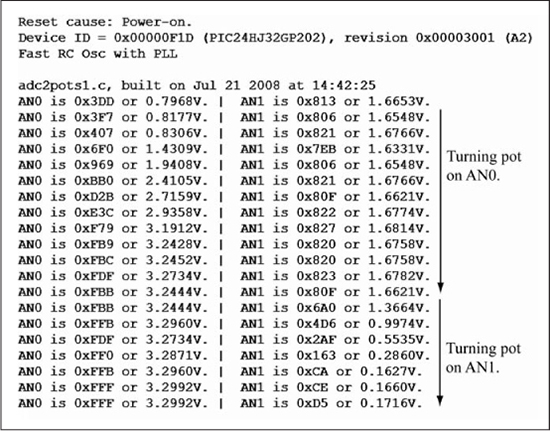
Note the changes in the ADC results on the last few readings in Figure 11.13. These readings were taken without adjusting the potentiometer settings. Recall that the ADC step size is very small, slightly above 800 μV. The difference in readings is likely due to noise and the dynamic comparator biases in the PIC24 ADC circuitry. It is very easy for these types of errors to be larger than 1 mV; therefore, ADC results are rarely “constant” when the conversion step sizes are so small. Finally, the 12-bit ADC result is typically too fine for use with many low-cost potentiometers. The low-cost pots, especially the “one-turn” pots, cannot generate voltages accurately enough for 12-bit conversion. The most significant eight bits of the ADC result are typically sufficient for these types of potentiometers.
PIC24 ADC Operation: Recap
As you have seen in the four simple ADC examples, the PIC24 ADC peripheral is complex and has many different features and operating modes. The four examples attempted to highlight the most common operating modes and are not intended to be comprehensive. The discussion and ADC examples are a starting point for your exploration of this powerful PIC24 μC peripheral. The operating modes shown in the four examples can be combined and used with other PIC24 ADC features not addressed. For example, the “Sample A” and “Sample B” settings (see AD1CON2.ALTS bit) can be used in conjunction with different channel scan select settings in the AD1CHS0 and AD1CHS123 registers to create complex ADC scan patterns. You are encouraged to spend quality time reading the sections on the PIC24 ADC in your device’s datasheet and in the PIC24 Family Reference Manual [21]. These references provide great insight into the ADC and showcase several useful combinations of PIC24 ADC features.
Digital-to-Analog Conversion
Just as there are many ways to convert an analog quantity to a digital code in an ADC, designers have invented many ingenious methods to convert a digital code back into an analog signal in DACs. Since DACs perform the complementary operation of ADCs, these two data converters have much in common. Like ADCs, the digital codes accepted by DACs follow many coding schemes, although unsigned and signed binary representations are the most popular. Furthermore, digital codes are provided to the DAC via many different communication protocols—fully parallel, serial via nibble-wide parallel transfers, and bit serial, including I2C, SPI, and many others. Also like ADCs, DACs exist that create different analog quantities for their output, but the most common is the voltage output DAC.
Like the ADCs, DACs are also characterized by a huge number of parameters. Many of the DAC parameters have the same names as the ADC parameters. However, the DAC parameters have a slightly different meaning as the two devices perform complementary functions. A DAC’s precision is the number of output levels that the DAC can create. Like the ADC, DAC precision is represented as the number of output levels or the number of bits required to encode the number of output levels. DAC resolution is the smallest distinguishable change in the output, and represents the change in output from a ±1 LSb change in DAC input. The DAC range is the total span over which DAC outputs can occur. DAC range can be computed through the DAC’s reference inputs; for example, range = (VREF+ – VREF–) for a voltage DAC. Obviously, the DAC has digital inputs so it must have a digital clock input to signal when the input sample data is valid. The time between each DAC conversion is the DAC’s period and is almost always the same as the ADC’s sample period. Assuming that the DAC in Figure 11.1 is an unsigned n-bit voltage output DAC with reference voltages VREF+ and VREF–, the DAC output y(t) is shown in Equation 11.2.
Although most DACs strive to create the input-output characteristic of Equation 11.2, the methods by which they achieve these results and the circuits they use vary widely. Each approach has advantages and disadvantages. You are encouraged to read about some of the other DAC architectures such as interpolating, charge sharing, current steering, and delta-sigma DACs. This chapter examines a DAC popular in small microprocessor applications: the R-2R flash DAC. A second DAC architecture, called a pulse-width modulation (PWM) DAC, is covered in Chapter 12 in conjunction with the timer discussion.
Sample Question: What is the voltage represented by an ideal 4-bit DAC with input 0xC and VREF– = 0 V and VREF+ = 4 V?
Answer: The DAC has a precision of 24 = 16 levels, and a range of (4 V – 0 V) = 4 V. The DAC input 0xC, or 12, will generate an output voltage of 0V + 12/16 × (4 V – 0 V) = 3.0 V.
Compare the reconstructed DAC result here with the ADC examples earlier in this chapter. The ADC input voltage 3.14159 V is converted to a 4-bit digital value 0xC. A 4-bit DAC using the same reference voltages converts the digital sample back into the voltage 3.0 V. The difference between the two voltages (e.g., 0.14159 V) is the quantization error. If you need voltage measurements that are more accurate, you need to use an ADC and DAC with more precision.
Flash DACs
A flash digital-to-analog converter, sometimes called a parallel DAC, is characterized by its capability to generate an output within a single clock cycle. The speed of a flash DAC is achieved by the parallel generation of a set of fixed references. The set of references is complete: it is capable of constructing all of the possible DAC output values. Thus, any desired voltage output can be created nearly instantly, making flash DACs very fast. There are many ways to go about creating these reference voltages, which gives rise to different flash DAC architectures. You will examine a reasonably hardware-efficient implementation for the resistor ladder flash DAC.
R-2R Resistor Ladder Flash DAC
The R-2R resistor ladder DAC also uses voltage division to generate the DAC’s output voltage, but does so in a clever way that uses relatively few resistors. Instead of generating all possible voltage outputs, the resistor ladder DAC effectively rearranges its voltage divider network based on the DAC’s digital input code. An n-bit R-2R resistor ladder flash DAC uses at least 2n resistors and n switches. The resistor ladder DAC uses a much smaller number of components than the same size resistor string flash DAC, especially as the DAC input code word length n gets large. The DAC’s digital input code bits control switches that make connections between resistors and virtually rearrange the resistor ladder network to form the DAC’s output voltage. The R-2R resistor ladder flash DAC is especially well suited for use with a small microprocessor like the PIC24 μC.
Just like all of the data converters that you have already examined, the resistor ladder DAC comes in many different word lengths. For discussion, let’s look at the 4-bit R-2R resistor ladder DAC in Figure 11.14. Once again, consider the unipolar implementation of the R-2R resistor ladder flash DAC to simplify the discussion and analysis. Bipolar implementations operate identically. The R-2R resistor ladder flash DAC uses four switches, three resistors of R ohms, and five resistors of 2R ohms. The four switches connect the appropriate power supply voltage to the 2R resistors.
Figure 11.14
R-2R resistor ladder flash DAC

The high reference voltage VREF+ is connected to each 2R resistor if the corresponding digital input code bit, X0, X1, X2, or X3, is 1. Otherwise, if the digital input code bit is 0, the lower supply voltage, usually ground, is connected to the appropriate 2R resistor. While not obvious, the switch states will create an output voltage that is proportional to the digital input code. The R-2R resistor ladder DAC in Figure 11.14 usually requires a voltage follower to prevent excessive current siphoning from the ladder that would cause voltage output errors.
To see how the resistor ladder DAC works, consider a few examples. Consider the case when the 4-bit input code, X3, X2, X1, and X0, is 0b0000. Since all 4 input bits are 0, each 2R resistor is connected to the lower supply voltage—ground in this example. The resistor ladder in Figure 11.15(a) has been redrawn to emphasize this fact. Obviously, the output voltage Vo must be 0 V since there is no other voltage source in the circuit.
Now, consider the case when the input code is 8, or 0b1000. Figure 11.15(b) shows the equivalent circuit when the input is 0b1000. Applying voltage division repeatedly gives Vo = VREF/2. When the input code is 0b0001, or 0x1, in Figure 11.15(c), repeated application of voltage division gives Vo = VREF/16. When the input code is 0b0010 = 0x2 as shown in Figure 11.15(d), you see that Vo = VREF/8. Since the R-2R resistor ladder DAC uses only linear resistors, the superposition theory applies.
Figure 11.15
Four-bit R-2R resistor ladder flash DAC example
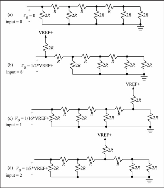
Superposition says that you can find a system’s response to several inputs by simply adding up the individual output responses to each input acting alone. Therefore, if the R-2R resistor ladder DAC in Figure 11.14 has more than one switch connected to VREF+, you can find Vo by summing the appropriate individual responses in Figure 11.15. For example, if the input code is 0b1001 = 0x9, the resistor ladder output voltage Vo is the sum of the responses at Vo for the two individual cases when the sources act alone. So, you find that Vo = VREF+/2 + VREF+/16 = 9 × VREF+/16. To generalize this result to an n-bit resistor ladder DAC, you find that for a digital input code of X, the resistor ladder output voltage Vo is (X/2n) × VREF+, which is the desired result. The resistor ladder DAC generates an output voltage that is linearly proportional to the digital input code.
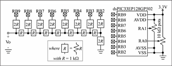
The resistor ladder DAC circuit in Figure 11.14 is actually much simpler to put into practice than it first appears. Switches and voltage supplies are not really needed because the PIC24 μC conveniently provides these in the form of digital output port pins. When the PIC24 μC is driving a 1 from one of its PIO pins, it is connecting that package pin to the PIC24 μC’s internal VDD. When the PIC24 μC is pulling down, or driving, its PIO package pin to 0, the PIC24 μC is really connecting that PIO pin to its internal ground. Therefore, the PIC24 PIO pins can be used to replace the switches, VREF+ = VDD, and ground connections in Figure 11.14. Therefore, the PIC24 μC can very easily build an 8-bit R-2R resistor ladder flash DAC with 16 resistors as shown in Figure 11.16. Simply writing the 8-bit value of the digital code X to correct bits of PORTB will create the voltage (X/256) × VDD at Vo. The resulting voltage is based on VDD because the PIC24 μC’s VDD is the resistor ladder DAC’s VREF+. Of course, any eight pins on the PIC24 PIO ports can be used instead of PORTB, and the DAC input word can be shorter or longer depending on the application. But beware: whenever you split the DAC input word across several IO ports, it will take several PIC24 μC instruction cycles to update the entire DAC value. During this time between output port writes, the DAC output voltage will likely be grossly incorrect. In practice, you would like to keep the R-2R output pins on the same PIO port and all bits adjacent and sequential, if at all possible.
Figure 11.16
Eight-bit R-2R resistor ladder flash DAC using IO port on dsPIC33EP128GP502
If the DAC’s load is purely capacitive or has a very large resistance, the circuit in Figure 11.16 works very well. However, the current flowing through the resistor ladder network is crucial to forming the voltage at Vo. Therefore, the R-2R resistor ladder DAC cannot be loaded by any circuit element that draws appreciable current. If a current drawing load is connected, the load will siphon current out of the resistor ladder and cause distortion at Vo. To prevent excessive current draw, you simply attach a voltage follower circuit at Vo. Furthermore, capacitance can be added to the voltage follower’s feedback path to create an active low-pass filter to smooth out the jagged stair-step pattern visible at Vo. The low-pass filter at a DAC’s output is sometimes called a reconstruction filter by digital signal processing experts.
Figures 11.17 and 11.18 list codes that create a simple sinusoid function generator with the PIC24 μC. The potentiometers on RA0 and RA1 control the sinusoid’s frequency and amplitude, respectively. The PIC24 internal ADC reads the voltage provided by a potentiometer every 100 ms. The relatively slow update is fine for this kind of user interface function. In operation, the PIC24 μC appears to respond instantly to the changes in potentiometer settings.
Figure 11.17
Code for DAC examples (part 1)

The code in Figures 11.17 and 11.18 uses the 16-bit Timer3 as a periodic interrupt source in a similar manner as previously done in Chapter 9. Timer3 is used to create periodic interrupts so that the R-2R resistor ladder DAC on PORTB can be updated at a uniform rate. At each Timer3 interrupt, the ISR writes an updated value to the DAC. A value from the sine lookup table, along with the 16-bit table lookup index value, are written to the DAC by the function call writeDAC(). The R-2R DAC in Figure 11.16 can only create one voltage, so you will soon see that the writeDAC() function for the R-2R resistor ladder DAC will ignore the second argument in its function call. (The DAC examples that follow this one will also use the code in Figures 11.17 and 11.18. Several of these DACs are capable of two channel output and will use the second argument passed to the writeDAC() function.)
Figure 11.18
Code for DAC examples (part 2)

The sine data in Figure 11.17 can be easily replaced with other values so that the PIC24 μC can create any arbitrary waveform like sawtooth and chirp signals. In fact, the lookup table can easily be changed to represent a single cycle of a saxophone recording making your PIC24 μC a simple music synthesizer. The lookup table au8_sine[] in Figures 11.17 contains 128 entries. Each entry is an 8-bit value representing the amplitude of a sinusoid at equally-spaced time intervals. The number of values can be increased to give the waveform more detail. The constant modifier for au8_sine[] tells the compiler that this array contains constant data (the array values are not changed), so this data is stored in program memory instead of data memory. This is useful especially for large lookup tables, which may not fit in data memory.
Upon its call, the timer ISR immediately updates the DAC value with the data sample calculated in the last ISR execution. Next, the timer index variable u16_idx is incremented with interval u16_per sensed by the code in main() from the user adjusting the potentiometer that controls the waveform frequency. As the user adjusts the pot, the number for u16_per increases and causes the u16_idx to traverse its 65,536 values more quickly. Every roll-over of the 16-bit variable u16_idx corresponds to the beginning of a new period of the sine wave. The ISR truncates the 16-bit u16_idx to a 7-bit index used to find the next sinusoid data value from au8_sinetbl. Then, the lookup table value is read into a variable and shifted based on the value in u8_amp. This right-shift provides very simplistic amplitude scaling. At the next interrupt, the computed DAC value is written to PORTB to update the waveform via the R-2R resistor ladder DAC in Figure 11.16.
Now that you have examined the big picture of generating a sinusoid waveform and controlling its frequency and amplitude via the two potentiometers, it’s time to look at the details of configuring the R-2R resistor ladder DAC in Figure 11.16. Figure 11.19 shows the subroutines to configure the R-2R resistor ladder DAC and to update the DAC value. Configuration of the R-2R resistor ladder DAC is simple: make each output port pin that drives a DAC resistor a digital output. Setting a bit on one of the DAC control pins is equivalent to pulling the corresponding 2R resistor up to VDD. Clearing a bit on one of the DAC control pins is equivalent to connecting the resistor to ground.
Figure 11.19
Configuration and update subroutines for R-2R resistor ladder flash DAC
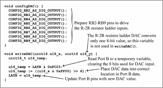
The function writeDAC() updates the register value and output pins that drive the 2R resistors in the R-2R resistor ladder DAC. Since you will only use eight of the 16 possible pins on PORTB, the function writeDAC() must take precautions not to change the eight bits in PORTB that the R-2R resistor ladder DAC does not use. The function writeDAC() starts by reading the current value of the PORTB register and clearing the eight bits that the DAC will modify. The eight-bit DAC value passed into writeDAC() is inserted into the correct position, then the new PORTB value is written to the IO port register. Figure 11.20 shows output from the circuit in Figure 11.16 running the code from Figures 11.17 and 11.19. At the bottom of Figure 11.20, you see the eight digital bits of data that drive the R-2R resistor ladder DAC along with the resulting analog voltage output.
Figure 11.20
Output of 8-bit R-2R resistor ladder flash DAC

External Digital-to-Analog Converter Examples
DACs can be constructed with any of the architectures introduced in the previous section and numerous other architectures not discussed in this book. DAC architecture selection is usually application specific. When choosing an external DAC, several options should be considered. The number and value of external reference voltages, word length, number of channels, input communication scheme, and chip package type are just a few. Many of these parameters are interrelated. If a single channel 24-bit DAC with parallel inputs is chosen, the DAC package will have at least 28 pins: 1 pin each for VDD, VSS, Vo, 24 pins for input data, and 1 pin for input latch or clock. If the DAC supports external reference voltages for the analog output or multiple output channels, the number of package pins rises quickly.
Parallel port IO pins are usually a microprocessor’s most limited and expensive resource since a chip package with a few more pins is far more expensive than the corresponding increase in silicon area costs to support those extra pins. Because parallel IO pins are so precious, many common external components choose to use pin-saving schemes for communication like the synchronous serial IO interfaces SPI and I2C introduced in Chapter 10. This section introduces an external DAC from Maxim Integrated Products that create analog voltages without consuming so many of the precious IO pins on the PIC24 μC. The DAC used in this example is the MAX548A, a dual 8-bit DAC with a SPI bus interface.
Using the PIC24 μC and this external SPI-connected DAC, you can combine concepts from this chapter and Chapter 10 to create an alternative, pin-conserving circuit to Figure 11.16 to create the sine wave output. The MAX548A is presented strictly as an example of connecting an external DAC chip to the microcontroller. Many other external DACs could have been used just as easily.
DAC Example: The Maxim548A
The Maxim Integrated Products MAX548A is a dual 8-bit DAC with a SPI-compatible interface. The MAX548A output is a voltage created by its internal R-2R resistor ladder DAC. The means by which the MAX548A creates its output is fundamentally identical to the discrete resistor R-2R approach in Figure 11.16; however, the MAX548A ladder resistors are accurately trimmed and matched during the manufacturing process. The MAX548A will produce a more accurate output voltage than the discrete resistor circuit. Furthermore, the MAX548A provides a second 8-bit DAC. Since the MAX548A is a SPI device, it gives you dual 8-bit DACs while using only three of the valuable IO pins. In contrast, the approach in Figure 11.16 would require 16 PIO pins for two 8-bit DACs.
The MAX548A is readily connected to the PIC24 μC; Figure 11.21 shows the details. To operate, the MAX548A requires three SPI signals from the PIC24 μC: SCLK, SDO, and a chip select. The MAX548A also requires the usual power supply connections, and the MAX548A signal LDAC# must be connected to VDD for these purposes. The MAX548A has two independent DACs and their outputs are the MAX548A pins OUTA and OUTB. The PIC24 μC controls the MAX548A by performing a single 16-bit SPI write transaction. However, you will implement the 16-bit write by two 8-bit writes due to the division of command and data between the two bytes. Figure 11.22 shows the details of the PIC24 μC communication with the MAX548A via SPI. For more information about SPI operations on the PIC24 μC, see Chapter 10. The MAX548A datasheet [68] contains more details about the MAX548A operation and limitations, and is required reading for anyone who wants to use the MAX548A in a design.
Figure 11.21
Interfacing the dsPIC33EP128GP502 microcontroller with a MAX548A DAC via SPI

Figure 11.22
Sample SPI operations for MAX548A DAC

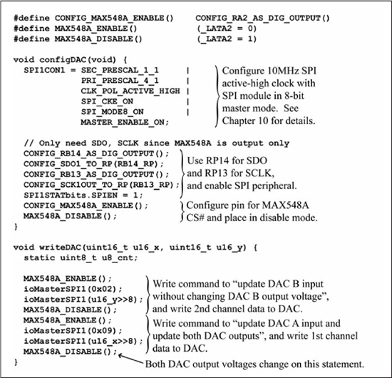
Using the MAX548A to create the sinusoid voltage output requires the same main() code as before—see Figures 11.17 and 11.18. Of course, the DAC configuration and update functions must be changed and made specific to the MAX548A. Figure 11.24 shows the code for the MAX548A. The MAX548A version of the function configDAC() begins by enabling the PIC24 μC SPI peripheral for 8-bit master mode operation with a 10 MHz SPI clock. The MAX548A requires no explicit configuration command, so you can progress to placing the MAX548A and the SPI bus into a normal operating state. Figure 11.21 shows the MAX548A active-low chip select pin, CS#, connected to the PIC24 μC IO pin RA2. Therefore, the function configDAC() configures the RA2 pin to be a digital output and initially disables the MAX548A. Two convenient macros, MAX548A_DISABLE() and MAX548A_ENABLE(), are defined in Figure 11.24 to improve code readability.
Figure 11.23
Command byte for the MAX548 DAC
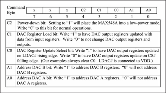
Figure 11.23 gives a brief description of the MAX548A command byte. Figure 11.24 shows the DAC function updateDAC() to write the new DAC values to both channels of the MAX548A. Updating both MAX548A channels is done in two SPI transactions. The first transaction writes the second argument of updateDAC() to the MAX548A’s second DAC. Notice that the MAX548 command byte of this first transaction disables the DAC register load operation by clearing the command byte’s bit 3, called C1 in the MAX548A datasheet. Clearing this bit allows you to write the contents of the DAC B register without changing its output. The second SPI transaction in updateDAC() writes the function’s first argument to the DAC A register and updates both DAC outputs simultaneously by setting bit C1 in the MAX548A command byte. Both SPI transactions in Figure 11.24 have the third bit, called C0, in the command byte cleared to instruct the MAX548A to update results on rising edges of CS#. Setting this bit would require you to connect a fourth PIC24 PIO pin to the MAX548A LDAC# pin.
Figure 11.24
Configuration and update subroutines for MAX548 DAC
Using the code in Figures 11.17, 11.18, and 11.24 with the circuit in Figure 11.21 generates a sinusoid output. The sinusoid waveform produced by the setup in Figure 11.21 is not reproduced here since it is identical to Figure 11.20. Furthermore, the output of the MAX548A’s second DAC generates a sawtooth waveform (from the second parameter passed to writeDAC(), which is the sine wave table index) whose frequency can be changed by the user via the potentiometer. The code in Figure 11.17 does not adjust the sawtooth waveform amplitude, but that could be added easily.
Summary
With the ever-decreasing cost of microprocessors, we are embedding digital computers into nearly every conceivable application. However, these digital computers must ultimately communicate with the “real world,” which is an analog environment. Data conversion with ADCs and DACs is done in nearly every microprocessor system that interfaces with other systems, especially other systems that involve people. The data conversion devices are so useful that many embedded microprocessors include built-in ADCs and/or DACs. An ADC gives the microprocessor the capability to understand and operate on analog values generated by people, sensors, or other systems. A DAC allows microprocessors to use its digital processing to create or recreate analog values that people, sensors, or other systems can understand. Even if a microprocessor does not have a built-in or suitable ADC or DAC, an external data converter can be acquired and connected to the microprocessor via a direct parallel connection, an address/data bus, or a serial communications scheme.
Review Problems
1. How many bits are required to represent a waveform in 4,000 discrete levels?
2. How many different input voltages could you detect with a 24-bit ADC?
3. An audio CD can contain 80 minutes of stereo (two independent) audio tracks. Each track is sampled with 16-bit samples at 44.1 kHz. How much audio information, in bytes, is stored on an audio CD?
4. What is the data throughput (in MB/sec) of the audio CD in problem 3? (Recall from Chapter 1 that 1 MB = 106 B.)
5. Still and movie images are often represented by an 8-bit value for each color component, red, green, and blue. How many different colors can be encoded?
6. An HDTV screen contains 1920 x 1080 pixels, with each red-green-blue (RGB) color component represented by eight bits of precision. Motion playback is 30 frames per second. How much storage is required to store the average two-hour movie? What is the data throughput during HDTV playback?
7. Assume a 4-bit successive approximation A/D with VREF+ = 4 V and VREF– = 0 V. Trace the steps for producing a 4-bit output code if the input voltage is 1.8 V.
8. For an 8-bit flash R-2R DAC, how many resistors of size R are needed? How many resistors of size 2R are needed?
9. A 3-bit flash A/D has seven comparators, and each comparator output can be either 0 or 1. Assume VREF+ = 4 V and VREF– = 0 V. What is the 7-bit output of these comparators if the input voltage is 2.7 V? Give the 7-bit value in binary, with the LSb corresponding to the comparator output with the smallest reference input and the MSb corresponding to the comparator with the highest reference input.
10. How many clock cycles would you expect a 12-bit successive approximation A/D to require for a conversion?
11. The VDD power supply is usually not used as a reference voltage for precision A/D measurements, as it varies with current load and temperature. The National Semiconductor LM4040 is a component that provides a stable 3.0 V voltage reference with an accuracy of 0.1%. What voltage values does this 0.1% correspond to? How does this voltage translate into a percentage of 1 LSb of the 10-bit value produced by the PIC24 μC using the LM4040 as a VREF+ value (assume VREF– = 0 V)?
12. For the PIC24 μC, assume an FOSC of 60 MHz. Using Figure 11.7, what FOSC configurations cannot be used because they violate the minimum A/D clock period of 75 ns?
13. A 10-bit ADC has a lower reference voltage VREF– of 0 V and an upper reference voltage VREF+ of 3.3 V. What output code corresponds to 0.449 V? To 2.91 V?
14. Repeat the previous problem for a 12-bit A/D and an upper reference voltage of 3.0 V.
15. An 8-bit DAC has a lower reference voltage of 0 V and an upper reference voltage of 3.3 V. What is the output voltage for codes of 0x7F? 0x4B? 0xCB?
16. A 10-bit DAC has a lower reference voltage of 0 V and an upper reference voltage of 3.3 V. What is the output voltage for codes of 0x7F? 0x14B? 0x3CB?
17. A 12-bit DAC has a lower reference voltage of 0 V and an upper reference voltage of 3.0 V. What is the output voltage for codes of 0x17F? 0x74B? 0xCCB?
18. The National Semiconductor LM60 is a precision Celsius temperature sensor. The LM60 produces an output voltage that is linear to the temperature in Celsius and equal to 6.25 mV/°C with an offset of +424 mV. The LM60 is accurate up to 150 °C. If your PIC24 μC is using internal ADC references and VDD = 3.3 V, determine the precision in °C of your measurements for the 10-bit and 12-bit operating modes.
19. Write a function that reads the LM60 discussed in the previous problem on an arbitrary PIC24 μC ADC input pin and returns the temperature to the calling function in a double data type. Your function should automatically determine and handle both 10-bit and 12-bit configurations.
20. How many bits of resolution are required for an ADC to measure the LM60 temperature (see problem 19) between 0 °C and 100 °C with a precision of 1.5 °C? Assume ADC reference voltages are 3.3 V and 0 V.
21. The code in Figures 11.17 and 11.18 creates a sinusoid waveform with amplitude control by logical shifts. While simple and efficient, this approach results in very abrupt amplitude changes as each control increment divides the current amplitude in half. Rewrite the code in Figures 11.17 and 11.18 to generate a sinusoid waveform with smoother amplitude adjustment. Your code should be compatible with all of the example DACs examined in this chapter. (Note: Floating-point arithmetic is CPU-intensive. Write your new code to use only integer operations.)