
CHAPTER 13
ADVANCED HARDWARE TOPICS
This chapter discusses various advanced hardware topics such as direct memory access (DMA), the Controller Area Network (CAN), and I2C multi-master operation. This chapter also discusses using the self-programming capability of the PIC μC for non-volatile data storage and use of the comparator module.
Learning Objectives
After reading this chapter, you will be able to:
![]() Use the direct memory access (DMA) capability for data transfer from peripheral modules.
Use the direct memory access (DMA) capability for data transfer from peripheral modules.
![]() Use the PIC24 μC as an I2C slave.
Use the PIC24 μC as an I2C slave.
![]() Discuss bus arbitration for multi-master busses and how bus arbitration is accomplished for CAN and I2C busses.
Discuss bus arbitration for multi-master busses and how bus arbitration is accomplished for CAN and I2C busses.
![]() Use two PIC24 μC as masters on an I2C bus.
Use two PIC24 μC as masters on an I2C bus.
![]() Compare and contrast features of the Controller Area Network (CAN) with the other serial interface standards used by the PIC24 μC.
Compare and contrast features of the Controller Area Network (CAN) with the other serial interface standards used by the PIC24 μC.
![]() Have the PIC24 μC use its program memory for data storage purposes.
Have the PIC24 μC use its program memory for data storage purposes.
Direct Memory Access
Direct memory access (DMA) refers to hardware-assisted data transfers between memory and peripherals (both on-chip and off-chip) with minimal CPU intervention. DMA reduces the CPU overhead for data transfer and can be used to aid both single burst and continuous transfers. Some members of the PIC24 family, such as the dsPIC33EP128GP502, have a flexible DMA controller module whose block diagram is shown in Figure 13.1. Because of the DMA module’s complexity, this section highlights a portion of the module’s features and shows one code example that uses DMA transfer. See the DMA section [44] of the FRM for full details. DMA memory transfers operate with no CPU stalls when using a special dual-ported SRAM memory (DPSRAM); although standard SRAM may also be used, this incurs the penalty of CPU stalls, where the CPU must wait until a DMA transfer completes and vice versa. The term dual-ported means that the DPSRAM can be accessed simultaneously by both the DMA module and the CPU without requiring either to wait. Data is either transferred from a peripheral to (DP)SRAM, or from (DP)SRAM to a peripheral as specified by registers within each DMA channel. A DMA channel can transfer in only one direction, and there is a natural priority with channel 0 being highest and 7 the lowest if simultaneous DMA requests occur.
Figure 13.1
DMA module block diagram.

Source: Figure redrawn by author from Figure 22.2 found in the PIC24 FRM (DS70223A), Microchip Technology Inc.
Each channel has the following registers:
![]()
DMAxCON: Control register for the DMA module.
![]()
DMAxREO: Associates a peripheral interrupt request with a channel.
![]()
DMAxSTAH/L, DMAxSTBH/L: (DP)SRAM starting address registers A and B; these registers specify starting locations in the (DP)SRAM for the transfer. These store a 24-bit bit address, which is divided into the upper 8 bits (DMAxSTAH, DMAxSTBH) and the lower 16 bits (DMAxSTAL, DMAxSTBL). In this book, the terms DMAxSTAH/L and DMAxSTA are used interchangeably; the same is true for DMAxSTBH/L and xSTB. Some transfer modes require register A or B, while others require both.
![]()
DMAxPAD: Contains the address of the peripheral data register involved in the transfer.
![]()
DMAxCNT: Specifies the number of transfers required to complete a DMA request; for N transfers, this must be initialized to a value of N - 1.
There are also five global registers (DSADR, DMAPWC, DMARQC, DMALCA, and DMAPPS) used for status information on the most recent DMA transfer (see the FRM [44] for more information). The DMAxCON register details are shown in Figure 13.2. The addressing mode (AMODE<1:0>) bits determine how a DMA address register steps through the (DP)SRAM buffer during a transfer. The default mode is post-increment, which means that the address buffer increments after a transfer. Once DMAxCNT+1 transfers have been performed when using post-increment mode, the DMA address register is at the end of the buffer and the address register is automatically reset back to the start of the (DP)SRAM buffer. This operates in the same manner as the head index used for the software FIFO discussed in Chapter 10. The addressing mode without post-increment always performs the transfer from the same location in (DP)SRAM. The peripheral indirect addressing mode is a special mode supported only by the ADC and ECAN™ (discussed later in this chapter) modules in which the peripheral provides the (DP)SRAM address for the transfer. The HALF bit determines if a DMA channel interrupt is generated after half of the transfers ((DMAxCNT+1)/2) have occurred, or after all of the transfers have been performed (DMAxCNT+1). DMA operation modes (MODE<1:0>) use either one (DP)SRAM buffer or two (DP)SRAM buffers (ping-pong mode) and are either one-shot or continuous. In one-shot single buffer mode, once DMAxCNT+1 transfers have been performed, the DMA module is automatically disabled (the CHEN bit in the DMAxCON register is cleared). In continuous mode, transfers continue as long as the module is enabled. The ping-pong mode implements the ping-pong buffering scheme discussed near the end of Chapter 10 (Figure 10.63). The first DMAxCNT+1 transfers use the DMAxSTA buffer, then the next DMAxCNT+1 transfers are performed using the DMAxSTB buffer. This allows the CPU to either fill or empty the DMAxSTA buffer while DMA transfers use the DMAxSTB buffer. After DMAxCNT+1 transfers are performed using the DMAxSTB buffer, then the next DMAxCNT+1 transfers are performed using the DMAxSTA buffer, and thus DMA transfers ping-pong between the DMAxSTA and DMAxSTB buffers. In one-shot ping-pong mode, the DMA module is disabled after DMAxCNT+1 transfers are done with both buffers. The null data write mode (NULLW bit is set) is a special mode intended for use with SPI receive transfers in which dummy data (a null data byte) are written to the SPI port to trigger each SPI receive. Without the NULLW mode, a second DMA channel would have to be used to feed null data bytes to the SPI port to generate the received SPI data.
Figure 13.2DMAxCON: Channel configuration register

Source: Figure redrawn by author from Register 22.1 found in the dsPIC33E/PIC24E FRM (DS70348C), Microchip Technology, Inc.
Figure 13.3 shows the details for the DMAxREQ register, which is used to associate a peripheral interrupt request with the DMA channel. When a peripheral’s interrupt request flag is set, this triggers the DMA transfer, which is typically how the DMA transfer is accomplished. However, the application can also force a transfer by setting the FORCE bit (DMAxREQ<15>).
Figure 13.3DMAxREQ: Channel IRQ select register

Source: Figure redrawn by author from Register 8.2 found in the dsPIC33EP128GP502 datasheet (DS70000657H), Microchip Technology, Inc.
The following steps are required for DMA setup:
1. Write the address of the peripheral’s data register used for the transfer to the DMAxPAD register so that the DMA module knows where to read or write peripheral data. Also write the DMAxREQ IRQSEL bits with the peripheral’s IRQ number.
2. Configure the peripheral module to set its interrupt flag for each requested data transfer. Because the DMA module cannot perform error checking during the transfer (such as detecting a parity error or framing error for UART receives), any error checking must be done by the application on an interrupt-driven basis (such as using the U1EIF flag and the _U1ErrInterrupt() ISR for UART1 RX error checking, see Figure 9.3 of Chapter 9).
3. Configure the DMAxSTA address registers and the DMAxSTB address registers (only for ping-pong modes) with the (DP)SRAM addresses for the transfers. The MPLAB PIC24 compiler has a convenient built-in function for accomplishing this, as you’ll see in the code example.
4. Initialize the DMAxCNT register with the number of transfers to accomplish.
5. Configure and enable the DMA module by writing to the DMAxCON register.
To illustrate DMA module usage, you’ll implement the streaming data application discussed in the last section of Chapter 10 that captures UART RX data and writes it to the 24LC515 serial EEPROM using DMA channel 0 in continuous ping-pong buffer mode. Figure 13.4 shows the C code for the DMA channel 0 configuration, the _U1ErrInterrupt() ISR, and the _DMA0Interrupt() ISR. The two buffers of Figure 10.63 that are used for capturing input data are implemented as DPSRAM buffers au8_bufferA and au8_bufferB, which are each 64 bytes. The space(dma) attribute requires these buffers to be located in the DMA DPSRAM memory space. The configDMA0() function accomplishes steps 1, 3, 4, and 5 of the channel 0 configuration, with step 2 (UART configuration) accomplished by the configDefaultUART() function called by configBasic() within main(). For step 1, the assignment
DMA0PAD = (unsigned int) &U1RXREG;
assigns the address of the UART1 RX register to the DMA0PAD register, causing the DMA module to read from U1RXREG for each transfer. Also in step 1, the assignment
DMA0REQ = DMA_IRQ_U1RX;
associates the UART1 RX receive interrupt with channel 0, triggering a DMA transfer for each received character. For step 3, the assignments
DMA0STAH = 0x0000;
DMA0STAL = __builtin_dmaoffset(au8_bufferA);
DMA0STBH = 0x0000;
DMA0STBL = __builtin_dmaoffset(au8_bufferB);
copy the DMA RAM addresses of buffers au8_bufferA and au8_bufferB to DMA address registers DMA0STA and DMA0STB. For step 4, the assignment
DMA0CNT = DMA_TRANSFER_SIZE - 1; // DMA_TRANSFER_SIZE is 64
sets the number of transfers to DMA_TRANSFER_SIZE, which is a value of 64, the size of each buffer. For step 5, the DMA0CON register is configured to enable the DMA module, place it in the continuous ping-pong mode, select a transfer direction of peripheral to buffer using post-increment buffer addressing, and to generate an interrupt after a buffer is full. The configDMA0() function also enables the UART receive error and DMA channel 0 interrupts. The _U1ErrInterrupt() ISR is triggered on a UART1 RX error and calls the checkRxErrorUART1() function, whose code was originally shown in Figure 10.13 and that generates a software reset on parity, framing, or overrun errors. The _DMA0Interrupt() ISR is triggered once a buffer is full and toggles the u1_bufferFlag that indicates which buffer is currently being filled by the DMA channel. The _DMA0Interrupt() ISR also sets the u1_writeFlag semaphore to inform main() that a buffer is ready to be written to the EEPROM.
Figure 13.4
DMA example code (part 1)

Figure 13.5 shows the main() code of the DMA example; this is a modified version of the EEPROM example main() code originally shown in Figure 10.60. This main() implements the flowchart of Figure 10.65, in which the write mode waits for a buffer to fill as indicated by the u1_writeFlag semaphore, then writes the full buffer to EEPROM as indicated by the u1_activeBuffer flag. The memWriteLC515() function used in this program has been modified from the original code shown in Figure 10.59 in that the data buffer contains only 64 locations and its first two locations are not reserved for holding the u16_MemAddr address. The modified memWriteLC515() function does not use the memWriteNI2C1() transaction function, but instead uses primitive I2C function calls to write the 64 data bytes to the EEPROM (the source code can be found on the book’s accompanying website). The read mode in Figure 13.5 simply reads bytes out of the EEPROM in 64-block quantities and then echoes them to the console. A pause mode for console output is toggled via console input.
Figure 13.5
DMA example code (part 2)

DMA can be very useful for reducing CPU overhead in streaming data applications such as audio input or output, or packet-oriented transfers such as Ethernet. For example, the while (1) loop of main() in Figure 13.5 only has to intervene when 64 characters are received, and could be performing some other task during the arrival of these bytes.
Using the PIC24 μC as an I2C Slave
In the I2C examples in Chapter 10, the PIC24 μC was always used as the bus master. However, the PIC24 μC can also function as an I2C slave, which is useful when embedding a μC within a product that requires an I2C interface. To illustrate this capability, we use the reverse string application that was originally given in Chapter 10 for demonstrating PIC24 μC operation as a SPI slave. The PIC24 μC master reads a string from the console and writes it to the PIC24 μC slave, which reverses the string as shown in Figure 13.6. The PIC24 μC master then reads the reversed string from the PIC24 μC slave and displays it on the console. In the SPI master/slave string example of Chapter 10, a PIO output from the slave was used as an output ready signal to the master to indicate when the reversed string was ready. In this example, the handshaking signal is dispensed with, as the master’s read transaction to the slave completes whenever the reversed string data is ready for transmission.
Figure 13.6
PIC24 μC Master to PIC24 μC slave using the I2C bus

Figure 13.7 gives the master code for the application of Figure 13.6. For I2C communication, an I2C address must be chosen for the PIC24 μC slave. Recall from Chapter 10 that the upper four address bits are manufacturer specific and allocated by Philips Semiconductor. The value 0x0 for the upper four address bits is the general call address and is used for broadcast transactions; devices can choose to respond to or to ignore this address. The value 0xF for the upper four address bits is a reserved address that should not be used. In this example, a value of 0x60 was arbitrarily chosen, as it was a free address on the I2C address bus in the target system and did not use an upper hex digit of 0x0 or 0xF. The while (1) loop of main() reads a string from the console and determines the string’s length. It then uses the writeNI2C1() function to perform an I2C block write to the slave, after which it immediately attempts to read the reversed string from the slave via the I2C block read function readNI2C1(). The block read waits after sending the address byte until the slave has the reversed string ready for transmit.
Figure 13.7
PIC24 μC master code for I2C string reversal application

The code for the I2C slave is interrupt-driven and uses the slave event’s interrupt flag (SI2CIF). The SI2CIF flag is set on I2C slave events, such as recognition of an address byte. The SI2C1IF flag is also set in a read transaction after an acknowledgement bit has been sent by the slave for a received data byte, and in a write transaction once a byte has been clocked out of the slave by the master and the acknowledgement bit sent by the master has been received by the slave. The master events interrupt flag (MI2CIF) is set by master events, such as completion of stop condition, start condition, repeated start, byte received or transmitted, acknowledgement transmitted, and bus collision. This implementation only uses the SI2CIF flag. The _SI2C1Interrupt() ISR code for the I2C slave is given in Figure 13.8, and contains four states. The initial state is STATE_WAIT_FOR_ADDR, which waits for an address byte whose upper seven bits match the seven bits in the slave’s address register I2C1ADD<6:0>. Once the SI2C1IF interrupt is generated, the STATE_WAIT_FOR_ADDR examines the R_W bit of the I2C1STAT register, which contains the R/W# bit of the received address. For a write transaction, the next state is WAIT_FOR_WRITE_DATA that reads the incoming byte from the I2C1RCV register, and places it in a buffer (sz_1[]). Once a null byte is received indicating the end of the string, the string is reversed and placed in buffer sz_2[] and STATE_WAIT_FOR_ADDR is reentered. If STATE_WAIT_FOR_ADDR detects a read transaction, it places the first byte of the reversed string in the transmit register I2C1TRN. It then sets the SCLREL bit high, which releases the clock line from a low state that is being held by the slave, allowing the master to generate clock pulses for reading the byte. The slave’s SCLREL bit is cleared automatically after reception of the address byte for a read transaction, or an ACK bit from the master after a read byte, indicating that more read data is expected from the slave. A 0 for SCLREL means the clock line is held low by the slave, generating an I2C bus wait condition. The bus wait causes the master to hang, unable to generate clock pulses until the bus wait condition is removed, giving the slave time to respond with data for the read operation. After the first byte of the reversed string is transmitted by STATE_WAIT_FOR_ADDR, the remaining bytes are transmitted by STATE_SEND_READ_DATA. When the null byte is loaded into the I2C1TRN register indicating the end of the reversed string, the next state is STATE_SEND_READ_LAST, which is an empty state to catch the interrupt generated after the null byte is clocked out. The read transaction is then finished, and the state transitions back to STATE_WAIT_FOR_ADDR. During a write transaction, an ACK bit is generated automatically for each received byte by the slave’s I2C module. A NAK is generated instead if the last received byte has not been read yet, or if a receiver overflow condition exists.
The main() code for the I2C slave is given in Figure 13.9 and it is rather simple in that all it does is configure the I2C module, initialize the I2C1ADD register with the chosen slave address, and enable the SI2CIF interrupt. The while (1) loop’s only task is to keep the heartbeat alive since the _SI2C1Interrupt() ISR performs the string reversal work. Figure 13.9(b) shows the master writing the string “MS” to the slave, with the slave returning the reversed string of “SM” in the following read transaction—see Figure 13.9(c).
Figure 13.8
PIC24 μC slave ISR code for I2C string reversal application

Figure 13.9
PIC24 μC slave ISR code for I2C string reversal application

Bus Arbitration for the I2C Bus
In the I2C bus introduction of Chapter 10, the formal definition of a bus was given as a communication channel in which there are one or more transmitters and multiple receivers. It was also stated that the I2C bus supports multiple bus masters (multi-master); in other words, any I2C device on the bus can initiate a transaction. However, the earlier examples always assume that the PIC24 μC is the sole bus master and the PIC initiates all I2C transactions. If a bus supports multiple bus masters, there must be a bus arbitration mechanism that decides which device assumes control of the bus when there are simultaneous attempts by different bus masters to access the bus. Figure 13.10 shows two common methods of bus arbitration for multi-master buses. In centralized arbitration (see Figure 13.10(a)), a device wanting to communicate on the shared bus requests permission to access the bus via a bus request (breq) signal to an arbiter, which grants the device the bus via the bus grant (bgrant) line.
In the case of simultaneous requests, the arbiter uses a priority scheme to choose which device is granted bus access. A fixed priority scheme has static priorities assigned to each device such as device #1 always having the highest priority and device #n the lowest. A fixed priority scheme can result in one device monopolizing the bus, so a rotating priority scheme is more common, in which priorities are dynamically rotated among devices in an attempt to provide equal access to the bus.
Figure 13.10
Two methods of bus arbitration

The disadvantage of centralized arbitration is that each device on the bus must have its own pair of bus request/bus grant lines. Centralized arbitration is most common in backplane busses found in computer systems that have a fixed number of I/O slots, and hence, a fixed number of devices that can be present on the bus.
Figure 13.10(b) shows an arbitration scheme called Carrier Sense Multiple Access/Collision Detection (CSMA/CD), which is useful when it is unknown a priori the number of devices that will be connected to a bus. In CSMA/CD, a device wanting bus access waits until the bus is idle, and then begins transmitting. If multiple devices transmit, there will be a data collision on the bus. A device must be able to sense a collision and then determine independently of the other devices what action to take. A transmitter detects a collision by sensing the bus state during transmission; if the bus state does not match what the transmitter is sending, a collision has occurred. Local area networks based on Ethernet use CSMA/CD; when a collision occurs all transmitters stop sending data, wait for a random interval (the backoff interval), and try again. The backoff interval is random to help ensure that one transmitter wins and the others lose the arbitration. If another collision occurs, the interval wait time is increased (typically doubled) and another random wait is performed. This continues until a transmitter is successful at gaining access to the bus. While this works, it also wastes time because of the need for all transmitters to wait for the random interval.
The I2C bus also uses CSMA/CD for arbitration, but resolves conflicts in a manner different from Ethernet. Figure 13.11 illustrates how arbitration is performed on the I2C bus. Assuming both CPUa and CPUb begin transmitting at the same time, the first data sent after the start condition is the address byte of the I2C slave device and simultaneously, a clock signal over the SCL line. A 0 on the SDA bus overrides a 1 because of the open-drain output used to drive SDA (and also SCL). Each device senses the SDA line during transmission; if a device detects that the SDA state is different from what it has transmitted, the device immediately ceases transmission, giving up the bus. In this example, CPUa is initiating a transfer to an EEPROM (address 1010????), while CPUb is beginning a transfer to a DAC (address 0101????). CPUa stops transmitting after it sends the first (most significant) bit of its address because the initial 0 sent by CPUb overrides the 1 sent by CPUa. Observe that CPUa’s transmission did not disturb CPUb’s transmission, so no data are lost and no time is wasted by the arbitration. What if both CPUa and CPUb attempt to write to the same device? Because the address bits are the same, the arbitration continues through the data bits, until either some difference is detected or the transaction completes if both devices send exactly the same data.
Figure 13.11
I2C bus arbitration

At this point, you should understand the reason for the pull-up resistors on the I2C bus; the drivers for the SDA/SDL lines are open-drain to permit multi-master bus arbitration by having a 0 state override a 1 state. This conflict resolution in CSMA/CD is simple and effective, and is used in other CSMA/CD busses, as you’ll see when the Controller Area Network is discussed in the next section.
Reverse String Revisited
The reverse string application of Figure 13.6 can now be revisited knowing that each PIC24 μC can act as both a master and a slave since the I2C bus is a multi-master bus. Labeling the left-hand PIC24 μC as CPU1 and the right-hand PIC24 μC as CPU2, when CPU1 sends the string to CPU2 then CPU1 is the master and CPU2 is the slave. After CPU2 reverses the string, it acts as a bus master and sends the reversed string back to CPU1, which responds as a slave. This is a better solution than originally provided in which CPU1 was always the master and CPU2 the slave, in that CPU2 sends the reversed string when it is ready, allowing CPU1 to process the input on an interrupt-driven basis. Figure 13.12 shows the _SI2C1Interrupt() ISR code, which is the same for both CPUs and stores a received string into a buffer (sz_1[]) and sets a semaphore (u8_gotString) once a complete string has arrived. The ISR uses the same state machine approach for processing an I2C write transaction as used in Figure 13.8.
Figure 13.12
ISR code for the multi-master reverse string application

The main() code for the multi-master reverse string application is given in Figure 13.13. The initialization code for both CPUs is the same, as the I2CADD register must be initialized and SI2CI interrupt enabled since both CPUs act as slaves. A macro named CPU_ID is used to conditionally compile code for either CPU1 or CPU2 within the while (1) loop and also for I2C address selection for the two CPUs. The CPU1 code reads a string from the console and uses the writeNI2C1() function to send it to CPU2. Following this is a wait on the u8_gotString semaphore, which indicates reception of the reversed string, which is printed to the console. The CPU2 code waits on the u8_gotString semaphore that indicates reception of the string sent by CPU1, which is then reversed by reverseString(). The reversed string is then sent back to CPU1 using the writeNI2C1() function.
Figure 13.13main() code for the multi-master reverse string application

The Controller Area Network (CAN)
The automotive market is important for microcontroller manufacturers, as a typical car or truck has tens of microcontrollers within it. The number of microcontrollers within vehicles keeps increasing as automobiles evolve to mobile computing platforms that happen to carry people between locations. An automobile is a harsh environment from an electrical noise perspective and contains electrical systems dispersed throughout the vehicle with communication distances measured in meters. CAN [46] is a half-duplex serial bus designed as a communication mechanism for intelligent peripherals within an automotive system. CAN’s signaling mechanism is designed to combat the inherent electrical noise found within vehicles. The CAN bus uses only two wires for communication, keeping electrical cabling size to a minimum, thus making it easier to route within the crowded compartments of an automobile. CAN is a true bus in the formal sense like I2C; CAN transactions are visible to all peripherals connected to the bus and each transaction includes an 11-bit identifier that is used by receivers to filter messages. The CAN bus is multi-master in that any node on the bus can initiate a transaction, with arbitration handled similarly to I2C arbitration.
Figure 13.14 shows a PIC24 μC with an internal CAN module connected to a CAN bus. A CAN bus is implemented as two wires, CANH/CANL, which uses differential signaling (discussed in Figure 13.15) to form a half-duplex communication channel. A transceiver chip like the Microchip MCP2551 [47] is required to convert from CAN bus voltage levels to CMOS logic levels (similar to the MAX3232 chip for the RS232 standard as discussed in Chapter 10). The enhanced CAN (ECAN™) module on a PIC μC has separate transmit (CxTX) and receive (CxRX) pins that are multiplexed by the CAN transceiver onto CANH/CANL. The CANH/CANL wires implement differential signaling; a pair of wires is used to signal a logic state, either 0 or 1. To this point, all signaling methods discussed in this book have been single-ended; one wire is used to signal a logic 0 or 1. The disadvantage of differential signaling is that it doubles the number of wires needed and as such is primarily used for serial transfers. The advantage of differential signaling is common-mode noise rejection, as shown in Figure 13.15.
Figure 13.14
PIC24 μC with CAN system

Figure 13.15
Common-mode noise rejection in differential signaling

Common-mode noise is noise (Vn in Figure 13.15) that is injected equally (or nearly so) onto all wires within a cable. A CAN bus within an automobile can be relatively lengthy and has ample opportunity to pick up noise from neighboring cable bundles or from other nearby systems. Any common-mode noise is rejected at the receiver as the two input signal voltages are subtracted from each other to form the received voltage. Differential signaling is commonly used in external cabling that carries high-speed signals outside of a computing system.
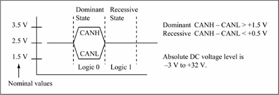
Non-return-to-zero (NRZ) asynchronous transmission is used on the CxTX/RxTX pins that connect the PIC μC to the transceiver of Figure 13.14. The differential signaling method used on the CANH/CANL wire pair is shown in Figure 13.16. A logic 1 is called the recessive state, and is defined as when CANH – CANL < +0.5 V. A logic 0 is called the dominant state and is defined as when CANH – CANL > +1.5 V. The recessive state (logic 1) is the bus idle state. The dominant state (logic 0) overrides the recessive state (logic 1); if one transmitter sends a 0 and a second transmitter sends a 1, the bus will contain a 0 state (the dominant state). Absolute DC voltage levels can range from –3 V to +32 V, and CAN transceivers such as the MCP2551 must be able to survive transient voltage surges of –150 V to +100 V. Data rates range from 10 Kbps to 1 Mbps with the maximum data rate limited by the CAN bus length. On a CAN bus, all CAN nodes must agree on the data rate.
Figure 13.16
CANH/CANL differential signaling
The physical signaling shown in Figure 13.16 is not defined by the CAN 2.0 standard, but rather by the ISO-11898 specification that was created to ensure compatibility between CAN nodes in an automotive system. This means that the CAN protocol can be used with different physical signaling methods as long as the CAN 2.0 specifications are met.
Data transmissions are sent in frames, with each frame split into fields, and with each field containing one or more bits, as shown in Figure 13.17. There are six different frame types: standard data, extended data, remote, error, overload, and interframe space. A standard data frame is shown in Figure 13.17(a). The start-of-frame bit (start bit) is a logic 0 that signals the beginning of a frame. The arbitration field contains an 11-bit ID and a 12th bit called the RTR bit, which is 0 for a data frame and 1 for a remote frame. An extended data frame, in which the IDE bit is a 1, has a 29-bit identifier, as shown in Figure 13.17(b). An identifier is not an address in the I2C sense; it does not have to uniquely identify either the sender or receiver. All nodes on the CAN bus receive the message; each node decides whether to act on the message based upon the value of the identifier and the contents of the message. The ECAN™ module for PIC μCs contains multiple filter/mask registers that are used to determine if a received frame should be accepted or rejected; these filter/mask registers use the ID field for accept/reject decisions. Once a frame has been accepted, it is transferred to an internal message buffer for further processing by the PIC μC application. The reason that message IDs function in this way is because many nodes on a CAN bus within an automobile are simple from a communication aspect in that they only periodically output sensor data (such as engine temperature), and there may be multiple nodes that are interested in this information. This message ID scheme provides efficient distribution of data to multiple receivers.

The ID field is used for multi-master arbitration in the same manner as I2C arbitration. A CAN node must wait until the bus is idle before attempting transmission. When multiple CAN nodes simultaneously attempt to transmit, they monitor the CAN bus as the ID field is sent. A 0 state (dominant) overrides a 1 state (recessive); a CAN module ceases transmission if it detects a difference between the CAN bus state and what it has transmitted. Like I2C bus arbitration, this results in no lost bus time or in any corrupted messages. The ID field is transmitted most significant bit to least significant bit so the message with the lowest numerical ID field wins during arbitration. This assigns a fixed priority to message identifiers. Arbitration is only performed on the ID field and the CAN specification does not define what occurs if two messages with the same identifier are sent simultaneously. As such, assignment of message identifiers within a CAN system must be done in such a way as to guarantee that simultaneous transmission of messages with the same ID does not occur (the CAN spec does define this case for a collision between a standard data frame and a remote data frame, and the RTR bit in the arbitration field determines priority in this case).
One strength of the CAN protocol is error detection. The cyclic redundancy check (CRC) field is a checksum based on the SOF, arbitration, control, and data fields that can detect a number of different errors, including five randomly distributed errors, any odd number of errors, and burst errors of less than 15 bits in length. The control field includes a message length so every frame received is also checked for the correct length, and each frame is also acknowledged by the receiver during the acknowledge field time (similar to the ACK bit in the I2C protocol, except this is for the entire frame).
Because of the large number of bits sent in one frame, there must be a mechanism that allows the receiver to remain synchronized to the bit stream or else cumulative error between transmitter and receiver clock mismatch will cause incorrect sampling of the received bits as originally discussed in Chapter 10. This is accomplished through a technique known as bit stuffing, shown in Figure 13.18. Bit stuffing is done by the transmitter, which adds an extra bit that is the complement of the preceding bit if it detects that five bits of the same value have been transmitted. This is done to guarantee that every 6-bit interval contains a data transition (a guaranteed transition density), which allows a phase locked loop (PLL) or digital phase locked loop (DPLL) circuit at the receiver to synchronize the sampling clock to the bit stream.
Figure 13.18
Bit stuffing in CAN

The bit stuffing and bit destuffing is invisible to the user and is done automatically by the transmit and receive hardware. Figure 13.18 shows an example where both a 0 and 1 are added by the bit stuffing logic to the data stream. Observe that the 1 did not actually have to be added to the bit stream to guarantee a transition in 6-bit intervals as a 1 was present in the bit stream after the five 0 bits. However, the bit stuffing logic does not know this and so the 1 bit is stuffed into the bit stream anyway. Bit destuffing by the receiver is the opposite procedure; if five bits of the same value are received, the next bit is assumed to be a stuffed bit and is removed from the data stream. Bit stuffing is also useful for bit-level error detection, as a stuck-at-0 or stuck-at-1 failure in the transmitter causes the bit destuffing logic to detect an error in the received bit stream when the received bit value does not match the expected polarity of a stuffed bit. The usage and formatting of the remaining frame types of remote frame, error frame, and overload frame are not discussed. Refer to the CAN specification for more information.
The PIC24 ECAN™ Module
A block diagram of the enhanced CAN (ECAN™) module on the PIC24 μC is given in Figure 13.19. The module uses message buffers residing in DMA RAM for transmit and receive: up to eight message buffers for transmit and up to 32 for receive. The 16 acceptance filters in the RX path can be flexibly configured for matching on either an 11-bit or 29-bit message identifier.
Because of the ECAN™ module’s complexity, we will not attempt to cover all of the ECAN™ module’s register details. Instead, we present an ECAN™ example and discuss some of the register usage as required by the example. We also use some utility C functions available on this book’s website, and discuss what the functions accomplish in terms of ECAN™ transfer but do not cover their code implementation. We encourage you to peruse the utility function’s code implementations in conjunction with the ECAN™ section [48] of the PIC24 Family Reference Manual for a deeper understanding of ECAN™ module details.
Figure 13.19
PIC24 ECAN™ block diagram

Source: Figure redrawn by author from Figure 21.2 found in the PIC24H FRM (DS70226B), Microchip Technology, Inc.
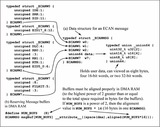
Figure 13.20(a) shows the ECANMSG type that the code example uses for a single message buffer, which is eight 16-bit words, or 16 bytes. Words w0, w1, w2, and w7 are used for the message identifier, control bits, and other status information. The data member contains the user payload of up to eight data bytes; the union64 data type allows the payload to be viewed as either uint8_t, uint16_t, or uint32_t items. Figure 13.20(b) shows how to declare a group of message buffers in DMA RAM. Because the DMA modules use peripheral indirect addressing (the ECAN™ module generates the address for the DMA), it is important that the DMA memory block be aligned to the nearest power of two that encompasses its size. The attribute aligned(NUM_BUF*16) does this as long as NUM_BUF is a power of two.
Figure 13.20
C data structure for message buffer
The code used to initialize DMA channels for ECAN™ transmit and receive is shown in Figure 13.21. Channels 0 and 1 are used (arbitrary choices), one for write (see Figure 13.21(a)) and one for read (see Figure 13.21(b)). Each channel uses peripheral indirect addressing in word mode, continuous operation. The transfer size is eight words, so DMA0CNT is initialized to 7. For ECAN™ transmit, the DMA peripheral address register (DMA0PAD) is initialized to the address of the ECAN™ transmit register (&C1TXD), and the DMA interrupt request (DMA0REQ) to DMA_IRQ_ECAN1TX (a value of 0x46). For receive, the same registers in channel 1 are initialized to the ECAN™ receive register (&C1RXD) and DMA_IRQ_ECAN1RX (a value of 0x22), respectively. In this example, the ECAN™ transmit and receive share the same buffer space, so the address registers (DMA0STA, DMA1STA) of both channels are initialized to point to msgBuf.
Figure 13.21
C data structure for message buffer

Figure 13.22(a) shows how the bit sampling is accomplished during data reception. The number of sampling clocks used for a bit time is programmable to be from 8 to 25 time quanta (TQ), with a single time quantum equal to a sampling clock period. The time quanta are distributed between the sync segment (always 1 TQ), propagation segment, phase segment 1, and phase segment 2. When a bit edge does not occur within the sync segment, resynchronization is achieved by either lengthening phase segment 1 or by shortening phase segment 2, with the amount of adjustment limited by a parameter called the sync jump width. The base clock (FCAN) for the TQ is derived from either FCY or FOSC and cannot exceed 70 MHz for the dsPI33E/PIC24E family. The data rate is given by Equation 13.1 with PRE representing the combination of two cascaded prescalers. One prescaler is fixed to divide by two, while the other is programmable, providing prescale (PRE) values of 2×1, 2×2, 2×3, ..., 2×64.
The baud rate initialization code for the ECAN™ module is given in Figure 13.22(b), which configures a 1 Mbps data rate using FCAN = 60 MHz, TQtotal = 30, and PRE = 2×1.
Figure 13.22
ECAN™ baud rate configuration

Figure 13.23 gives details on C utility functions used for ECAN™ configuration. The listed functions are for ECAN™ module 1; the same functions exist for ECAN™ module 2. The CHANGE_MODE_ECAN1() function is used to change operating modes; this example makes use of the configuration and loopback modes. The configTxRxBufferECAN1() function is used for configuring the first eight buffers (buffers 0 through 7) as either TX or RX buffers; any buffers higher than buffer 7 can only be used for RX.
The configRxFilterECAN1() function is used for configuring one of the 16 available RX filters as specified by u8_filterNum. A filter can optionally be used in combination with one of three mask registers (0, 1, or 2). If a mask register is not used, then an exact match is needed between the ID stored in the filter register and the incoming message for the message to be accepted. If a mask register is used, then a 0 in a mask register bit makes that bit a don’t care for filter matching. If a match is made, the message is accepted and stored in the message buffer specified by u8_bufnum, which accepts values between 0 and 14. A message buffer value of 15 specifies that the RX message be placed in the RX FIFO, which is discussed later. The configRxMaskECAN1() function is used for configuring one of the three available mask registers.
Figure 13.23
Configuration utility functions
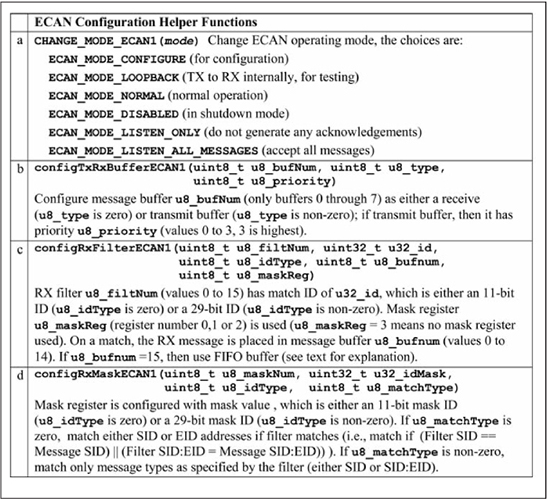
Figure 13.24 gives some utility functions for transmit and receive operations. These will be covered in the context of the C code that uses them.
Figure 13.24
Transmit, receive utility functions

Configuration code that uses the functions of Figures 13.21 through 13.24 is shown in Figure 13.25. The ECAN1 module is first placed into configuration mode via CHANGE_MODE_ECAN1(ECAN_MODE_CONFIGURE) (see Figure 13.23). The baud rate is then configured for 1 Mbps assuming FCAN = 60 MHz by the configBaudECAN1() function (see Figure 13.22). The configRxFilterECAN1() function call configures filter #0 for an 11-bit identifier match on MSG_ID (value of 0x7A0, arbitrarily chosen) and uses mask register #0 in the match. Buffer RX_BUFFER_ID (a value of 1) is used to store the incoming message on a match. The configRxMaskECAN1() function call configures mask register #0 for an 11-bit mask ID type that has a value of 0x7FC, and to only match the filter ID type (which is also set as an 11-bit ID). The last two bits of the mask register value 0x7FC are zero, which means that the last two bits of an 11-bit ID are not used in the match, allowing a range of message IDs to be accepted (in this case, message IDs of 0x7A0, 0x7A1, 0x7A2, and 0x7A3 are accepted). Only two message buffers (msgBuf[NUM_BUFS]) are allocated, one for TX and one for RX, which is the minimal number to support both transmit and receive. The configTxRxBufferECAN1() function is used to mark buffer #0 as a TX buffer and buffer #1 as an RX buffer. Finally, the DMA channels are configured using the configDMA0() and configDMA1() functions of Figure 13.21.
Figure 13.25
ECAN™ configuration code

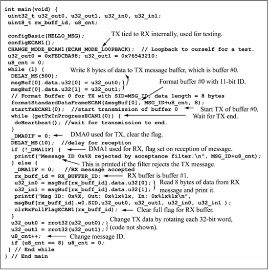
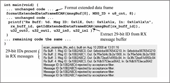
Figure 13.26 shows the main() code for testing the ECAN1 module. The loopback mode is used for testing, which ties TX back to RX internally. The while (1) loop places eight bytes of test data into message buffer #0 then uses the formatStandardDataFrameECAN() function to format the message with an 11-bit message ID. The while (1) loop generates message IDs in the range of 0x7A0 through 0x7A7. The mask register value of 0x7FC causes messages 0x7A0 through 0x7A3 to be accepted since the upper nine bits of the message ID matches the upper nine bits of filter #0, while other message IDs are rejected. The startTxECAN1(0) function call causes buffer #0 to be transmitted. Transmission is finished once getTxInProgress(0) returns as zero. A small software delay is used to wait for the message to be received; if the _DMA1IF flag remains cleared after the delay then the TX message was rejected by the acceptance filters, and an appropriate message is printed to the console. If the _DMA1IF flag is set, then the message was accepted, and the message ID and message contents are read out of the RX message buffer (buffer #1) and are printed to the console. The clrRxFullFlagECAN1(rx_buff_id) function call is used to clear the full flag of buffer #1.
Sample output from the test code of Figure 13.26 is shown in Figure 13.27. As expected, messages with IDs of 0x7A0 through 0x7A3 are accepted, while other message IDs are rejected.
Figure 13.27
Console output for ECAN™ test

Using an ECAN™ RX FIFO
The previous example used the minimum number of DMA buffers, one each for RX and TX, and assigned an acceptance filter to a single RX buffer. The ECAN™ module also has the capability of assigning multiple RX buffers arranged in a FIFO order (see Chapter 10 for a discussion of a FIFO buffer structure) to an acceptance filter. Figure 13.28 shows the code changes to the previous example required to configure the ECAN™ module to use a seven-element FIFO for RX messages. The number of message buffers is increased from two to eight, with one buffer used for TX (buffer #0) and seven for RX (buffers #1 through #7). In configECAN1(), the C1FCTRL register that controls FIFO operation is configured for the FIFO to start at buffer #1 and continue to the end of the buffer space. The RX_BUFFER_ID that is used to assign filter #0 to an RX buffer is changed from a value of 1 to a value of 15, which indicates that this filter is to use the FIFO capability for storing messages. In the RX code for main(), the GET_FIFO_READBUFFER_ECAN1() function is used to determine the buffer number that has the current RX data; this buffer number is printed with the rest of the RX data.
Figure 13.28
Code changes for using a seven-element FIFO

Figure 13.29 shows sample output using the seven-element RX FIFO; observe that RX messages are placed in buffers #1, #2, ... #7 and then receive wraps back to buffer #1.
Figure 13.29
Sample output using RX FIFO

Using an Extended Data Frame
Figure 13.30 shows the changes required to the RX FIFO code of Figure 13.28 to use an extended data frame (supporting a 29-bit message ID) instead of a standard data frame (which has an 11-bit message ID). The configRxFilterECAN1() and configRXMaskECAN1() function calls within configECAN1() are changed to configure the filter and mask registers for 29-bit IDs instead of 11-bit IDs. Within main(), the formatExtendedDataFrameECAN() function is used to format the TX message buffer with a 29-bit ID, and the RX printf() statement uses the getIdExtendedDataFrameECAN() function to extract the 29-bit message ID from the RX message buffer.
Figure 13.30
Code changes for using an extended data frame

Run-Time Self-Programming
In Chapter 10, an external serial EEPROM was used as an example of I2C interfacing and provided off-chip non-volatile data storage. The PIC24 μC is also capable of self-programming its own program memory, in a process known as run-time self-programming (RTSP) [50]. This offers a convenient non-volatile storage mechanism, provided that there is free space in program memory (also referred to as flash memory). RTSP also offers a way for a PIC24 μC to upload a new program via a communication port; the code that is executed during this process is called a bootloader and resides in some protected space that is not overwritten by the new program. Flash memory is erased one page at a time, where one page is 512 instructions (recall that an instruction is three bytes, or 24 bits). A flash page is organized in 8 rows of 64 instructions and flash memory can be written as either an entire row or a single instruction. Write and erase operations are self-timed, which means the operations take a variable amount of time depending on environmental and power supply conditions, as well as the number of previous erase/write cycles. Minimum page erase time is 20 ms, while minimum row and word write times are 1.6 ms and 20 μs, respectively. When using flash memory for storing data, one must be cognizant that the number of flash erase/write cycles before possible failure is finite; the PIC24 μC datasheet for a typical processor gives 10,000 as the minimum number of guaranteed write operations (the write endurance). Conversely, the 24LC515 serial EEPROM used in Chapter 10 has a maximum erase plus write time of 5 ms and a minimum write endurance of 1,000,000 cycles. These parameters and an application’s requirements generally determine whether an external or internal non-volatile memory solution is needed.
Recall from Chapter 6 that the program space visibility (PSV) capability allowed program memory to be mapped into the data memory as a method of accessing program memory data. The disadvantage of this method is that only the lower 16 bits of each instruction word are available via PSV since data memory is 16 bits wide. In RTSP, a different mechanism for accessing program memory uses table read/write instructions (see Figure 13.31) that allow access to all 24 bits of an instruction. The tblrdl (table read low) instruction accesses the lower 16 bits of an instruction, while the tblrdh (table read high) instruction reads the upper eight bits. The source address register (Ws) specifies the lower 16 bits of the program memory address (the offset) for the read, while the upper bits are contained in the TBLPAG special function register. The table write instructions, tblwrl and tblwrh, write the lower 16 bits and upper eight bits of the instruction respectively. The lower 16 bits of the program memory destination address is specified in Wd, while the upper eight bits are contained in TBLPAG. The TBLPAG register must be initialized with the upper bits of a program memory address before a table read/write instruction is executed.
Figure 13.31
Table read/write instructions

The table write instructions do not write directly to program memory, but rather, to an intermediate row latch. Flash memory program and erase operations are controlled by the NVMCON special function register, with details shown in Figure 13.32. An erase or write cycle is started by setting the WR control bit, which first requires a special unlock sequence similar to that used by the OSCCON register for changing oscillator options. These code examples use the PIC24 compiler built-in function __builtin_write_NVM(), which executes the unlock sequence and sets the WR bit.
Figure 13.33 shows the first set of utility functions for performing RTSP. The doWriteLatchFlash() function writes u16_wordhi:u16_wordlo (only the lower 24 bits are valid) to the row latch at the program memory address specified by u16_addrhi:u16_addrlo. The doReadLatchFlash() function returns the content of a program memory location as a uint32_t from the address specified by u16_addrhi:u16_addrlo.
Figure 13.32
NVMCON register details

Source: Figure redrawn by author from Register 5.1 found in the dsPIC33E/PIC24E FRM (DS70609D), Microchip Technology Inc.
Figure 13.33
C utility functions for RTSP (part 1)

A page erase at location u16_addrhi:u16_addrlo is accomplished by the doErasePageFlash() function; observe that the value of 0x4003 written to the NVMCON register within doErasePageFlash() enables flash modification by setting the WREN bit and specifies a page erase by setting NVMOP = 0b0011.
The erase is started by a series of asm statements to unlock the NVMCON register, followed by setting the WR bit to a 1. Two nop instructions later, the code then monitors the WR bit status and does not exit the function until it is cleared, indicating that the erase is finished. Interrupts are disabled during the function call to __builtin_write_NVM() because the unlock sequence enables a write to the WR bit for only one instruction cycle, and thus cannot be interrupted in order for the unlock to succeed. The doWriteRowFlow() function writes the current row that has been loaded via table write operations; its structure is similar to doErasePageFlash().
Utility functions that write and read one page of flash memory are given in Figure 13.34. The doWritePageFlash() function writes u16_len bytes of data stored in buffer pu8_data to flash address u32_pmemAddress. This function erases the page before writing, which is generally needed since once a bit has been programmed to a 0 condition, it cannot be returned to a 1, except by an erase operation (flash memory is all 1s after an erase). The doReadPageFlash() function reads u16_len bytes into buffer pu8_data from flash address u32_pmemAddress. Both functions use the union32_t data type that offers convenient access to the low and high words of a 32-bit value, which is needed when passing the u32_pmemAddress to the utility functions of Figure 13.33.
A Sample Flash Application
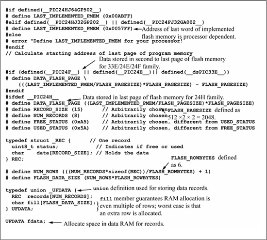
A typical usage of flash memory is to store N fixed-length records, where the record data and format is application dependent, such as bar codes, RFID tag values, fixed-length ASCII strings, and so on. Figure 13.35 shows a union data structure named UFDATA that stores NUM_RECORDS of size RECORD_SIZE, whose format is defined by the REC structure. Each record has a byte that indicates a status of free (FREE_STATUS) or used (USED_STATUS), and a data member that can store RECORD_SIZE bytes. Records are stored in the last page of flash memory as specified by DATA_FLASH_PAGE, whose value is processor dependent. The DATA_FLASH_PAGE value is calculated by taking the address of the last word of program memory, dividing by 1024, truncating, then multiplying by 1024. The value 1024 is the number of program memory addresses occupied by 512 instructions (512 × 2 = 1024, recall that one 24-bit instruction appears to occupy two program memory addresses). If this code is to be used on a PIC24F, PIC24E, or dsPIC33E processor, then it should be modified such that the data is stored on the second to last flash page, since the last flash page for these processors contain a packed version of the configuration bits that are copied to the configuration registers after each reset (configuration bits in the PIC24H family are stored in a special area of flash memory that is not used for program memory). The fill member of UFDATA is included to guarantee the data RAM allocation for UFDATA is a multiple of the row size, since the doWritePageFlash() function makes this assumption. All records are stored in data RAM, using the global variable fdata. The strategy is to make record modifications in data RAM using the fdata variable and write the data to flash memory when you want to make the changes permanent.
Figure 13.34
C utility functions for RTSP (part 2)
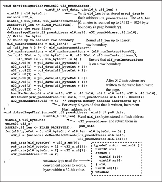
Figure 13.35
Data structure for flash application
Utility functions for record manipulation are given in Figure 13.36. The doFormat() function marks all records as FREE_STATUS, and is used to initialize the record array. The doCommit() and doRead() functions write all records to flash memory and read all records from flash memory, respectively. The doDelete() function marks the record specified by u16_recnum parameter as free. The doInsert() function copies data from the sz_1 parameter into the first free record, and marks that record as used. There is also a doPrint() function, which is not shown, that prints all the records to the console.
Figure 13.36
Utility functions for record manipulation

Figure 13.37 shows the doMenu() function that provides for testing of the flash utility functions by allowing record data to be entered from the console. The main() function is also shown, which calls doMenu() after standard initialization.
Figure 13.37
Flash application test function

Console output from testing the flash application is given in Figure 13.38. Two strings are entered as record data, followed by a write of the record data to flash memory. After a power cycle, the record data is read from flash memory and printed, illustrating that the records were successfully stored to non-volatile memory.
Summary
This chapter surveyed some advanced topics concerning on-chip peripherals for the PIC24 μC. The I2C and CAN busses are similar in that both are multi-master and both perform bus arbitration by using open-drain drivers with a 0 bit being dominant over a 1 bit in terms of winning the arbitration. Run-time self-programming allows program memory to be used as non-volatile data storage by a user application.
Figure 13.38
Flash application console output

Review Problems
1. If two I2C bus masters access the same device on the bus simultaneously, one using a read transaction and one using a write transaction, which CPU wins the arbitration? (Assume that the only difference in the first byte of the transaction is the R/W# bit.)
2. If two CAN bus masters access the bus, one with an 11-bit message ID of 0x4A0 and one with an 11-bit message ID of 0x3F2, which CPU wins the arbitration?
3. If an acceptance filter on the PIC24 μC is set for an 11-bit ID message ID match with a value of 0x615 and it also uses a mask register whose value is 0x71F, what range of message IDs are accepted?
4. Assume the 16-bit value 0xFF00 is transmitted on the CAN bus (use MSb first). Draw the serial waveform after bit stuffing has been done.
5. Assume the 16-bit value 0xF803 is transmitted on the CAN bus (use MSb first). Draw the serial waveform after bit stuffing has been done.
6. Using typical erase and write times, how much time is required to erase and write the entire flash memory of the dsPIC33EP128GP502 neglecting software overhead and data that is written one row at a time?
7. Look up the specifications for the PIC24HJ256GP206. Assume you want to use the last page of its flash memory for storage of non-volatile data. What would the value of FIRST_UNIMPLEMENTED_PMEM (first unimplemented program memory location) be for this processor, as defined in Figure 13.35?
8. Look up the specifications for the PIC24HJ128GP204. Assume you want to use the last page of its flash memory for storage of non-volatile data. What would the value of FIRST_UNIMPLEMENTED_PMEM (first unimplemented program memory location) be for this processor, as defined in Figure 13.35?
The next two questions are best assigned as short reports.
9. Do research on the LIN (local interconnect network) bus and answer the following questions.
a. How many wires does it need?
b. Classify it as duplex, half-duplex, or simplex.
c. How is addressing to devices handled?
d. What are the signaling levels?
e. Is it synchronous or asynchronous?
f. What is the maximum transfer speed?
g. What is the maximum number of devices allowed on the bus?
10. The system management bus (SMBus) is a two-wire bus that was derived from the I2C standard by Intel in 1995. It is currently used in PC motherboards and various microcontrollers. Download the SMBus specification (http://smbus.org/specs) and answer the following questions.
a. Give a couple of key differences between SMBus and I2C. For the key differences you chose, give the reasoning behind these changes.
b. Can you give an advantage of SMBus over the I2C bus? Defend your answer.
c. Are the I2C devices used in Chapter 10 compatible with the SMBus? Defend your answer.