
CHAPTER 10
ASYNCHRONOUS AND SYNCHRONOUS SERIAL I/O
This chapter discusses some of the serial interfaces available on the PIC24 μC: the Universal Asynchronous Receiver Transmitter (UART), the Serial Peripheral Interface (SPI), and the Inter-Integrated Circuit (I2C) bus. The protocols and operational modes of these three interfaces are discussed in detail along with interfacing examples to different external devices. Chapter 13 discusses the more complex Controller Area Network (CAN) serial protocol.
Learning Objectives
After reading this chapter, you will be able to:
![]() Describe the differences between synchronous and asynchronous serial data transfer.
Describe the differences between synchronous and asynchronous serial data transfer.
![]() Draw the waveform for an asynchronous serial data transfer that includes a start bit, data bits, and stop bits.
Draw the waveform for an asynchronous serial data transfer that includes a start bit, data bits, and stop bits.
![]() Write C code that sends and receives asynchronous serial data via the UART subsystem.
Write C code that sends and receives asynchronous serial data via the UART subsystem.
![]() Discuss the signals and signaling levels associated with the EIA RS-232 interface.
Discuss the signals and signaling levels associated with the EIA RS-232 interface.
![]() Write C functions for performing interrupt-driven receive and transmit for the PIC24 UART.
Write C functions for performing interrupt-driven receive and transmit for the PIC24 UART.
![]() Compare and contrast the SPI and I2C synchronous serial I/O protocols on the PIC24 μC.
Compare and contrast the SPI and I2C synchronous serial I/O protocols on the PIC24 μC.
![]() Interface a PIC24 μC to a digital thermometer using the SPI protocol.
Interface a PIC24 μC to a digital thermometer using the SPI protocol.
![]() Interface a PIC24 μC to a digital potentiometer using the SPI protocol.
Interface a PIC24 μC to a digital potentiometer using the SPI protocol.
![]() Implement PIC24 μC to PIC24 μC communication using the SPI protocol.
Implement PIC24 μC to PIC24 μC communication using the SPI protocol.
![]() Interface a PIC24 μC to a digital thermometer using the I2C protocol.
Interface a PIC24 μC to a digital thermometer using the I2C protocol.
![]() Interface a PIC24 μC to a serial EEPROM using the I2C protocol.
Interface a PIC24 μC to a serial EEPROM using the I2C protocol.
![]() Use interrupt-driven double buffering to implement continuous data stream applications.
Use interrupt-driven double buffering to implement continuous data stream applications.
I/O Channel Basics
Parallel I/O uses a group of signals for data transfer, with a clock or data strobe signal typically used for controlling the transfer. Figure 10.1(a) shows a 16-bit parallel I/O link between CPU_a and CPU_b, with a clock signal used to perform one data transfer each clock cycle. The bandwidth of a communication channel is usually expressed either as the number of bytes transferred per second (B/s) or the number of bits transferred per second (b/s). Observe the capitalization difference between Bps (bytes/second) and bps (bits/second); Bps is related to bps via the relationship Bps = bps/8. For Figure 10.1(a), the bandwidth is 600 MB/s if the clock frequency is 300 MHz, because two bytes are transferred each clock cycle. Data sent one bit at a time is called serial data transfer, and Figure 10.1(b) shows a synchronous serial interface that uses a single bit line with a separate clock to accomplish the transfer. The bandwidth of this channel is 1/16th that of the bandwidth of Figure 10.1(b), because the 16 data lines have been replaced by only one data line. The advantage of parallel I/O is obvious: it has n times the bandwidth of a serial channel, assuming both channels use the same data transfer rate and the parallel channel has n data lines.
Figure 10.1
Parallel versus serial I/O

The principal advantage of serial I/O is that it is cheaper to implement in terms of integrated circuit, cable, and connector pin count than parallel I/O. This is especially important for microcontroller applications in which cost is typically an important constraint: fewer external pins used to communicate with external devices can lower the overall cost of the final product. In other applications, serial I/O is typically used for data transfer between devices that require external cabling, such as between a keyboard and a personal computer. This is because a serial cable requires fewer wires than a parallel cable, which reduces the cost. It also makes the cable less bulky and reduces the physical connector size, which is an issue when there are multiple I/O cable connections to a device. In addition, wires within an I/O cable are subject to crosstalk, defined as a voltage change on a wire inducing a voltage change in a neighboring wire. Crosstalk can corrupt data transfers, resulting in an unreliable communication channel. Crosstalk increases with cable length and with higher signaling speeds. Methods for combating crosstalk increases the cabling costs, and thus serves as another reason for reducing the number of signals in an I/O cable. Parallel I/O is typically used for high-bandwidth, short-distance communication between integrated circuits in the same system.
High bandwidth, low cost, and reliable transfers are desirable properties of any I/O channel. Unfortunately, these properties conflict with each other: increasing bandwidth typically increases cost and decreases the reliability of the I/O transfer. Increasing I/O channel bandwidth can be done by any combination of the following actions:
1. Increase the number of signals carrying data; e.g., increase a parallel I/O channel from 8 bits to 16 bits.
2. Decrease the amount of time between data transfers; e.g., increase the clock speed of the I/O channel.
3. Use a signaling method that encodes more data in the same time interval; e.g., use a four-level voltage signaling method so that 2 bits are encoded in each signaling interval (00 = 0 V, 01 = 1/3 VDD, 10 = 2/3 VDD, 11 = VDD).
Methods 1 and 2 are the most common ways used to increase I/O channel bandwidth. Doubling the number of signal lines in an I/O channel doubles the bandwidth, but it also doubles the cost of the I/O channel. Decreasing the time used for each transfer increases bandwidth, but also increases the complexity of the electronics used for driving and receiving data signals, increasing the cost of each data signal. One method of decreasing the time between transfers is to use reduced voltage swing on the data lines instead of requiring the data signals to transition fully between VDD and ground. Swinging a data line by 200 millivolts to indicate a change from 1 to 0 or vice versa is accomplished faster than requiring a signal to transition from 0 to VDD.
Figure 10.2 defines the terms simplex, half duplex, and duplex in reference to communication channels. A simplex channel allows data transfer in one direction only. A half-duplex channel supports transfer in either direction, but in only one direction per data transfer. A duplex channel (also referred to as full duplex) supports transfers in both directions simultaneously.
A physical connection between two systems is either a unidirectional wire (transfer in only one direction) or a bidirectional wire (transfer in either direction). In Chapter 8, you saw that tristate buffers are required to implement a bidirectional port. A single unidirectional wire can implement a simplex channel, while a single bidirectional wire can implement a half-duplex channel. Two unidirectional wires can implement a duplex channel with each wire providing communication in one direction. A more complex electrical signaling method known as current-mode signaling can be used to implement a duplex channel using a single wire. However, use of current mode signaling is rare; all of the devices discussed in this book use voltage-mode signa ling.
Figure 10.2
Simplex, half-duplex, and duplex communication channels

Synchronous, Asynchronous Serial I/O
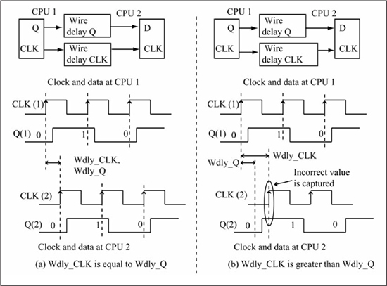
Synchronous serial I/O either sends a clock as a separate signal, as shown in Figure 10.3(b) or uses a scheme that allows the receiver’s clock to remain synchronized to the bit stream. Sending a clock as a separate signal is an intuitive solution for synchronous I/O, but at high signaling speeds wire delay becomes significant, especially in external cabling. If the wire delays of the serial data wire and clock signal are significantly mismatched, the active clock edge can clock in the wrong data bit at the receiver as is seen in Figure 10.3(b).
Data/clock wire delay mismatch becomes larger the faster the signaling speed and the greater the distance. The Controller Area Network (CAN) serial transmission standard discussed in Chapter 13 uses synchronous transmission and is intended for serial communication over cables of several inches/centimeters to several feet/meters. Because of this, its signaling methods do not send a separate clock signal, but uses a different method for maintaining synchronization as discussed further in Chapter 13. The I2C and SPI serial interfaces on the PIC24 μC, which are discussed later in this chapter, use synchronous transmission, and they all use the signaling method of Figure 10.1(b) that sends the clock with the data as a separate signal. This is because these interfaces are intended for short-distance communication between integrated circuits on the same printed circuit board. The separate clock also simplifies the logic implementation, which was important for older serial interfaces such as I2C and SPI that were defined in the 80’s because logic gates for an on-chip serial interface required a larger percentage of the total chip area at that time than it does today.
Figure 10.3
Synchronous serial I/O: sending the clock with the data
Asynchronous Serial I/O Using NRZ Encoding
Asynchronous serial I/O does not send a separate clock signal, and various signaling schemes are used to allow the receiver to read the serial data. Some schemes use a two-wire signaling method in which neither wire is a clock in the traditional sense, with transitions encoded on the wires in such a way that allows serial data to be extracted and supports dynamically varying transmission rates. This method is used by the high-speed serial I/O standard known as IEEE 1394, or FireWire.
Another asynchronous method that uses only a single wire encodes serial data as non-return-to-zero (NRZ), which means that a high voltage is used for a 1 bit and a low voltage is used for a 0 bit. The serial line remains at either a high or low state when successive bits of the same value are sent. The NRZ format is the most intuitive format used for serial data encoding; other schemes exists such as bi-phase encoding that uses different edge transitions for distinguishing 1 and 0 bits (discussed in Chapter 12). Asynchronous NRZ serial transmission is what the PIC24 μC reference system of Chapter 8 uses for communication over the serial link to the attached personal computer.
Because a separate clock signal is not sent with the serial data, there is no issue of wire delay mismatch between clock and data, so asynchronous NRZ serial transmission can be used for long distance (meters/feet) communication. The disadvantage of asynchronous NRZ serial transmission is that it has a lower maximum data rate when compared to advanced synchronous signaling methods, for reasons to be discussed later in this section.
In an asynchronous NRZ serial transfer, the sender and receiver agree on a common data rate and a common data format in terms of how many data bits are sent for each transfer. Figure 10.4 shows an asynchronous NRZ serial data frame. Before transmission begins, the line is in the idle or mark condition, which is a logic 1. The time required for sending one bit is referred to as a bit time. The start of transmission is indicated by a transition from the idle condition to logic 0, known as the space condition. This first bit, which is always a logic 0, is called the start bit and enables the receiver to detect the beginning of a transmission. Data bits are sent in the order of least significant bit (LSb) to most significant bit (MSb), with common data formats being 7 data bits + even/odd parity (discussed later in this section) or 8 data bits with no parity. The transmission ends with at least one stop bit, defined as the line remaining at 1 for at least one bit time. A total of 10 bit times are required for 1 start bit, 8 data bits, and 1 stop bit. Frame formats are identified as “(data size including parity bit, parity type, # of stop bits),” with E, O, N used for even parity, odd parity, and no parity, respectively. Thus, the frame format of Figure 10.4(a) can be (8, O, 1) if odd parity is used or (8, E, 1) if even parity is used.
Figure 10.4
Asynchronous data frame

A parity bit is a bit added by the sender to provide error detection of single-bit errors. Parity is either even or odd. The value of an even or odd parity bit is chosen so that the total number of 1 bits in the n data bits + parity bit is even or odd, respectively. For example, if a 7-bit data field is 0b0101101, which contains an even number of 1s, odd parity selects a parity bit of 1, resulting in an odd number of 1 bits. In contrast, even parity selects a parity bit of 0, resulting in an even number of 1 bits. The receiver checks the value of the parity bit. An incorrect parity indicates that some type of transmission error has occurred. A single parity bit is guaranteed to detect any single bit error; that is, if only one bit of the n data bits + parity is received in error, the parity scheme detects that an error occurred. If multiple bit errors occur, the parity scheme might not detect the error. Figure 10.5 gives three examples of asynchronous serial data frames.
Figure 10.5
Example of asynchronous serial data frames

In Figure 10.4, each bit is sent within its own distinct signaling interval. This book refers to the signaling interval as a bit time, with the number of bits per second (bps) of the link given by Equation 10.1.
Another term commonly used for the signaling speed of an asynchronous serial link is baud rate, whose definition is the number of signaling events per unit time. If only one bit is sent per signaling interval, baud rate is equal to bits per second. However, if more than one bit is sent per interval, such as a four-level voltage signaling scheme that sends two bits per signaling event, then bits per second is twice the baud rate. This book only discusses signaling methods in which one bit is sent per signaling interval, so baud rate is used interchangeably with bit rate.
Figure 10.6 shows how phase and frequency differences between receiver and sender clocks are handled. Given a data rate of y bps, the clock used by the sender/receiver for accessing the serial data is a multiple of this rate, usually 64x, 16x, or 4x. Assuming a 16x clock, when the receiver detects a start bit (high to low transition), it counts 8 clock periods and then captures the input value.
After this point, the receiver samples the input line every 16 clock periods, placing the sampling point near the center of the bit interval, giving the receiver maximum tolerance for mismatch between receiver and transmitter clocks. Over time, any receiver/transmitter clock mismatch shifts the sampling point away from the bit time midpoint, eventually causing a reception error when the sampling point is shifted out of a bit interval. Sampling at the midpoint of the bit time gives a 50% error margin, or ±8 clock periods about the center of the clock interval. For a frame with 10 bit times, this gives a 50%/10 = 5% error tolerance in sender/receiver clock mismatch. This is an optimistic mismatch assumption; a more pessimistic calculation accounting for rise and fall times of the input signal and maximum phase mismatch uses only a 30% margin (approximately ±5 clock periods about the midpoint). This gives an error tolerance of 30%/10 = 3% error tolerance for sender/receiver clock mismatch. Observe that the error tolerance decreases linearly as the number of bit times in the frame increases; for this reason, asynchronous transmission frames are typically limited to 10 bit times. The cumulative error begins at zero on the next start bit transition since that is when the receiver begins counting internal clocks to determine the bit sampling position. The edge transition of the start bit is said to resynchronize the receiver to the bit stream. Cumulative error is not a problem for synchronous serial data transmission, which can send an unlimited number of bits per frame because the receiver remains synchronized to the serial input stream. Thus, even if asynchronous and synchronous serial channels have the same bit time, the synchronous channel has a higher effective data transfer rate because it does not have the overhead of the start and stop bits sent for every 8 data bits of the asynchronous transmission.
Figure 10.6
Phase and frequency differences between receiver and sender clocks

Figure 10.7 shows a software-based asynchronous serial data link. Two PORTB pins, RB2 (STX) and RB3 (SRX), implement transmit and receive, respectively, forming a duplex communication channel. The outCharSoft(uint8_t u8_c) function sends the 8-bit u8_c value serially from LSb to MSb using one stop bit. The doBitDelay(uint16_t u16_baudRate) function delays for one bit time. Observe that the outCharSoft() function assumes that STX is already in the idle (high) condition before sending the start bit. After sending the 8 data bits, the stop bit is sent, leaving the STX output in the idle condition.
The inCharSoft() function returns an 8-bit value from the serial link by first waiting for a start bit (SRX becomes a 0). Once a start bit is detected, the doBitHalfDelay(uint16_t u16_baudRate) function waits until the middle of the bit time. It then loops eight times, delaying a full bit time and then reading the SRX input. The function delays for an additional full bit time before exiting to account for the stop bit (it does no checking to ensure that the received stop bit was a one). Software-driven serial links using parallel port bits can work well, but their maximum performance is limited by the accuracy of the delay functions used to implement bit delays. Also, even though the separate TX and RX lines of Figure 10.7 have the capability of implementing a duplex channel, the outCharSoft()/inCharSoft() functions as written cannot perform duplex communication. This is because all of the CPU’s resources are either spent transmitting or receiving a character; it cannot do both simultaneously using the functions of Figure 10.7. One solution to this problem is to use dedicated hardware to implement the TX/RX functionality, as seen in the next section.
Figure 10.7
A software-based asynchronous serial data link

Sample Question: For asynchronous serial transmission, with 1 bit sent per signaling interval, what is the bit time in microseconds for a baud rate of 57,600?
Answer: From Equation 10.1, you know that:
bit time = 1/baud_rate = 1/57,600 = 1.736 × 10-5 s × 106 μs/s = 17.36 μs.
Sample Question: Assume a data format of 7 data bits + even parity. What is the parity bit value for the data 0x2A?
Answer: 0x2A = 0b010 1010 (7 bits); the number of 1 bits is odd, so the even parity bit value is 1.
The PIC24 UART
The PIC24 μC has an on-chip peripheral called the Universal Asynchronous Receiver Transmitter (UART, pronounced “you-art”) that implements an asynchronous data transceiver. For asynchronous transmission, a write to a special function register is all that is required in terms of CPU resources; the UART handles the details of sending the start, data, and stop bits. For asynchronous reception, the UART automatically shifts in any serial data it receives then sets a status flag indicating that data is ready. All the CPU has to do at that point is read a special function register to receive data.
The UART subsystem, like others found on the PIC24 μC, uses special function registers in two different ways: either as data registers or as control registers. Data registers are either used for transferring data from the subsystem to the external pins (a write operation to an external device), or for transferring data from the external pins to the subsystem (a read operation from an external device). Control registers contain a mixture of configuration and status bits. Configuration bits specify the operating mode of the subsystem, while status bits indicate the operational state of the subsystem. PIC24 microcontrollers can have multiple UARTs (UART1, UART2, . . . UARTn) with identical capabilities, so their register names have a number (x) that designates its associated UARTx. For example, register UxTXREG is the data transmit register, and its name for UART1 is U1TXREG. This code refers to named bits in UART registers by their fully qualified structure reference (register.bitname) to make the functions portable to PIC24 microcontrollers with multiple UARTS, which do not have macros defined for individual UART register bits. The dsPIC33EP128GP502 used in this reference system has two UART modules.
Figure 10.8 shows the UxMODE register that contains various control bits for UARTx transmit and receive operation. Figure 10.9 show the UxSTA register that contains both status and control bits for UARTx operation. You will learn about these various bits in the context of UART transmit, receive, and clock generation operations.
Figure 10.8
Ux MODE: Mode register

Source: Figure redrawn by author from Register 2.1 found in the dsPIC33E/PIC24E FRM UART datasheet (DS70000582E), Microchip Technology Inc.
Figure 10.9
Ux STA: Status and control register

Source: Figure redrawn by author from Register 2-2 found in the dsPIC33E/PIC24E FRM UART datasheet (DS70000582E), Microchip Technology Inc.
UARTx Transmit Operation
As previously mentioned, the UxTXREG is the data output register for UARTx. This register is actually the entry point for a four-entry first-in, first-out (FIFO) buffer for the UxTSR register that performs the shifting of serial data through the UxTX pin, as shown in Figure 10.10. Together, the UxTXREG FIFO and the UxTSR register form a five-entry buffer. The UTXBF read-only status bit in Figure 10.9 is 0 if a free location is available in the UxTXREG buffer. The UTXBF status bit must be checked before any write is done to TXREG, as data written to a full buffer is not accepted. The UART subsystem supports either 8-bit or 9-bit operation, which is why the UxTXREG FIFO is shown as being 9 bits wide. The 9-bit operation mode is useful if the TX output goes to two different devices in a multi-processor system as the 9th bit is treated as an address bit. The code examples use 8-bit mode; see the dsPIC33E/PIC24E Family Reference Manual (FRM) [22] for more information on 9-bit operation. In 8-bit mode, the supported data formats using control bits from Figure 10.8 are even/odd/no parity, with either one or two stop bits. The same frame format is used for both transmit and receive.
Figure 10.10
UARTx transmitter block diagram

Source: Figure redrawn by author from Figure 5.1 found in the dsPIC33E/PIC24E FRM UART datasheet (DS70000582E), Microchip Technology Inc.
UARTx Receive Operation
Figure 10.11 shows the UARTx receiver block diagram. Serial data enters via the UxRX pin and the receiver block automatically shifts the data into the UxRSR register upon detection of a start bit. The UxRSR contents are transferred to the UxRXREG buffer after stop bit reception. As with the UxTXREG, the UxRXREG is actually a four-entry buffer, with the read-only status bit URXDA (receive buffer data available bit UxSTA<0>) is 1 if data is available. The OERR bit (receive buffer overrun error status) is set to a 1 on reception of the stop bit of the fifth data word when the receive buffer already contains four data words. Data reception is inhibited until the OERR bit is cleared by the user, which clears all UxRXREG buffer contents as well as the UxRSR register. You must empty the buffer contents before clearing OERR if the buffer contents and UxRSR register value are to be preserved. The FERR bit (framing error status) is set to a 1 if the stop bit for the currently available word was read as a 0 instead of a 1. The PERR bit (parity error status) is a 1 if a parity error was detected for the currently available word. Both the FERR and PERR bits should be read before reading UxRXREG, as they reflect the status for the currently available word.
Three other pin functions associated with the UART are BCLKx, UxRTS#, and UxCTS#. The BCLKx pin can be used to output the 16x baud rate clock, while pins UxRTS# and UxCTS# are used for hardware flow control when transmitting or receiving serial data. The UARTEN (UART enable, UxMODE<15>) bit must be a 1 to enable the UART receiver block, with the UEN bits (UxMODE<9:8)>) further configuring the UxRX, UxTX pin operation. This code uses UEN = 00, which is the simplest operation mode, and disables the BCLKx, UxRTS#, and UxCTS# pin functions. See the dsPIC33/PIC24 FRM [22] for more information on using the hardware flow control features of the UART.
Baud Rate Configuration
The baud rate (BR) for the UART is controlled by the baud rate clock generator and is calculated by Equation 10.2. The UxBRG register is the period register for a 16-bit timer. High- and low-speed modes are selected by the BRGH (high baud rate select bit, UxMODE<3>) configuration bit, with BRGH = 1 used for high-speed mode and BRGH = 0 used for low-speed mode.

The low-speed mode uses a 16x clock for sampling each bit time and can reach lower baud rates before exceeding the 16-bit range of UxBRG. The high-speed mode only uses a 4x clock for sampling each bit, but can reach higher baud rates than the low-speed mode. Equation 10.3 solves Equation 10.2 for UxBRG because PIC24 applications need the UxBRG value that is required to achieve a particular baud rate.
Figure 10.11
UART receiver block diagram

Source: Figure redrawn by author from Figure 7.1 found in the dsPIC33E/PIC24E FRM UART datasheet (DS70000582E), Microchip Technology Inc.
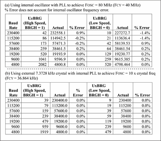
Figure 10.12(a) shows UxBRG values for FCY = 40 MHz assuming use of the internal oscillator and PLL for some standard baud rates. The % Error column shows the actual baud rate achieved without rounding of the UxBRG value, but does not include error due to inaccuracy of the internal oscillator frequency. In theory, either high-speed mode or low-speed mode should be adequate because of the small percent error values. This code uses the low-speed mode because in practice we have found this mode to be the most reliable when using the internal oscillator. Figure 10.12(b) shows the use of an external 7.3728 MHz crystal with the PLL to obtain an internal FCY = 36.864 MHz (five times the crystal frequency). This “strange” crystal frequency provides perfect matching to standard baud rates, and thus the % Error column values are zero. This is one reason why the base internal oscillator frequency is 7.37 kHz; an FOSC using this frequency or a division of this frequency provides better matching at higher baud rates.
Figure 10.12
UxBRG values for common baud rates
Using the PIC24 UART with C
Support functions for the UARTx subsystems are defined in the files libinclude pic24_uart.h and libsrcpic24_uart.c. Figure 10.13(a) shows the uint8_t inChar1() function, which waits for a byte to be available in UART1 and then returns it. The IS_CHAR_READY_UART1() macro simply returns the U1STAbits.URXDA status bit, which is 1 if data is available in the receive buffer. The checkRxErrorUART1() function in Figure 10.13(c) checks the PERR, FERR, and OERR error status bits, and calls the reportError() function with an appropriate error message (recall that reportError() saves the error message in a persistent variable and then executes a software reset—the resulting error message is printed by the printResetCause() function). The checkRxErrrorUART1() function must be called before data is read from the U1RXREG register because the error bits reflect the status of the currently available byte in the receive buffer. The outChar1(uint8_t u8_c) function in Figure 10.13(b) writes the byte in u8_c to the UART1 transmit buffer once space is available. The IS_TRANSMIT_BUFFER_FULL_UART1() macro is used to check for space availability in the transmit buffer by returning the U1STAbits.UTXBF status bit, which is 1 if there is at least one free spot in the transmit buffer. Similar functions for UARTs 2, 3, and 4 are defined, with conditional compilation used to include the functions only if the target device supports those UARTs.
Figure 10.13inChar1/outChar1 UART functions

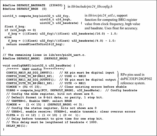
Figure 10.14 shows functions for UART configuration. The utility function compute_brg() computes a 16-bit value for the UxBRG register using Equation 10.3 based on function parameters that specify the clock rate (u32_fcy), speed mode choice (u16_brgh) and desired baud rate (u32_baudrate).
The configUART1(uint32_t u32_baudRate) function does UART1 register and pin configuration. The function configures the U1RX and U1TX pins to use RB10 and RB11 pins, respectively, on the reference dsPIC33EP128GP502 system of Chapter 8. The compute_brg() function is called to compute the value needed by the U1BRG register to achieve the desired baud rate. The U1MODE and U1STA registers are configured to enable UART1 receive and transmit using a data format of 1 stop bit, no parity, and 8 data bits with no hardware flow control (that is, it does not use pins UxCTS# or UxRTS#).
Figure 10.14
UART configuration
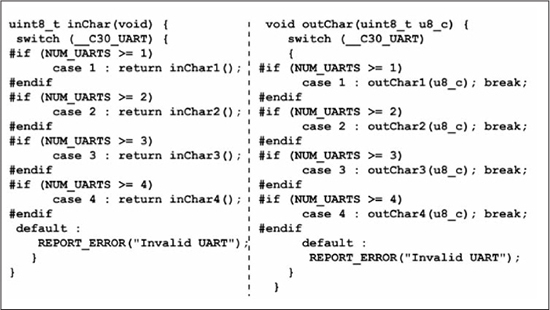
The various character I/O functions used thus far in these example programs such as outString(), outUint8(), inChar(), and so on, are contained in the file libsrcpic24_serial.c. Figure 10.15 shows the uint8_t inChar() and void outChar(uint8_t u8_c) functions used for single character input/output in pic24_serial.c. Observe that the global variable __C30_UART determines the UARTx destination by selecting between inChar1, inChar2, and so on for inChar() and selecting between outChar1, outChar2, and so on for outChar(). Thus, the character I/O functions contained in pic24_serial.c can be dynamically switched between the available UARTs on a PIC24 microcontroller.
Figure 10.15inChar()/outChar() serial I/O functions
<stdio.h> Library Functions
The C <stdio.h> library functions supported by the PIC24 compilersuch as printf, scanf, and so on can also be used either with the functions in pic24_serial.c or in lieu of these functions. By default, the <stdio.h> character I/O functions map to UART1 but there is a general mechanism in the PIC24 compiler for redirecting these functions to other peripherals—see the PIC24 16-bit Language Tools Libraries manual that comes with the compiler for more details. As stated previously, the examples here use a lightweight set of serial I/O functions because of the relatively large code footprint of the <stdio.h> library, but this point may be moot if you are using a PIC24 μC with a large program memory. The examples occasionally use the printf function when they need to take advantage of its advanced formatting capabilities.
Interrupt-Driven I/O with the PIC24 UART
As previously discussed, the receive and transmit components for the PIC24 UART can each buffer five bytes, four in the hardware FIFO and one in the shift register associated with the appropriate UxTX/UxRX pin. The receiver can experience buffer overrun if the UART receive buffer is not polled often enough by calling inChar(), while the outChar() function can waste clock cycles by waiting for a free location in the transmit buffer. Interrupts provide a more efficient method for performing UART I/O for both receive and transmit operations.
Interrupt-Driven UART Receive
Figure 10.16 shows an example application that reads a string from the UART using the inString() function, reverses the string using the reverseString() function, then sends the reversed string to the UART. In this application, a string arriving from the UART is considered terminated by either a new line or a carriage return (see the source files available from www.reesemicro.com for code details on inString() and reverseString()). The problem with this application is that while a string is being reversed and then printed, another string may be arriving. As long as strings are typed manually from the console, as seen in Figure 10.16(b), the while (1) loop can finish reversing and printing a previous string before arrival of a new string causes a UART overrun error. However, if multiple strings are pasted into the console application from the paste buffer, then strings arrive too fast and UART receiver overrun occurs—Figure 10.16(c)—causing a processor reset when the checkRxErrrorUART1() function of Figure 10.13 detects the overrun error.
Figure 10.16
String reverse application

Fast bursts of input data on a communication channel can cause overrun problems if polled I/O is used on the channel. One solution to this problem is to use interrupt processing on the channel for reading data as soon as it is available then storing it in a temporary buffer until it can be read by the application. Within the UART receiver, the UxRXIF interrupt flag in Figure 10.11 is set by various data available conditions, as determined by the URXISEL<1:0> bits (UxSTA<7:6>) of Figure 10.9. The _UxRXInterrupt ISR is associated with the UxRXIF interrupt flag and can be used to read the UARTx receiver when data is available, instead of relying on inChar() to poll for data availability. (Using the cell phone analogy from Chapter 9, the phone rings when a call is available instead of you having to continually check the phone to see if somebody is trying to talk to you.) However, where does the _UxRXInterrupt ISR place the data after reading the UxRXREG register? The answer is a software FIFO, which operates like the hardware FIFOs of Figures 10.10 and 10.11 except that data memory locations are used for storage.
Figure 10.17 shows the structure and operation of a software FIFO with eight locations. Two indexes, named head and tail, are used for accessing the buffer. The FIFO is empty when head is equal to tail. Data is written into the buffer by incrementing the head index then storing data at buffer[head]; see Figure 10.17(b). This means that data is available in the buffer whenever head is not equal to tail. Data is read from the buffer by incrementing tail then accessing data from buffer[tail]; see Figure 10.17(c). Observe that data comes out of the buffer in the same order in which it is placed into the buffer; hence the first-in, first-out (FIFO) designation. Figure 10.17(d) shows the buffer holding several characters. When the head index reaches the end of the buffer, the next write operation must wrap the head index to the beginning of the buffer; see Figure 10.17(e). For this reason, this data structure is also referred to as a circular buffer. In Figure 10.17(f), the write operation leaves the head index equal to the tail index, causing the buffer to appear empty even though it contains eight valid data items. This is buffer overrun, which means that under these rules for buffer insertion and extraction, an n-location buffer can hold a maximum of n – 1 data elements.
Figure 10.17
Software FIFO structure and operation

Figure 10.18 shows the implementation of the UART RX software FIFO in libsrcpic24_uart.c. If the UART1_RX_INTERRUPT macro is defined, then the interrupt version of inChar1() is compiled instead of the polled version shown in Figure 10.13(a). The most convenient place to define the UART1_RX_INTERRUPT macro—Figure 10.18(a)—is in the MPLAB® X project associated with the application’s source files. The UART1_RX_FIFO_SIZE and UART1_RX_INTERRUPT_PRIORITY macros—Figure 10.18(b)—set the FIFO buffer size and interrupt priority, respectively, and can be overridden by the user. The inChar1() function now waits for data to be available in the buffer, indicated by u16_rxFifo1Head being not equal to u16_rxFifo1Tail; see Figure 10.18(c). When data is available, the tail index is incremented and wrapped if necessary, and the new data is returned from au8_rxFifo1[u16_rxFifo1Tail]. The _U1RXInterrupt ISR is triggered when data is available in the receive buffer. The head index is incremented and wrapped if necessary, as shown in Figure 10.18(f), and if head is equal to tail then a buffer overrun error is reported which resets the processor; see Figure 10.18(g). If no overrun is present, the new data is placed into the buffer at au8_rxFifo1[u16_rxFifo1Head]. The configUART1() function of Figure 10.14 is also modified to enable the U1RXIF interrupt when the UART1_RX_INTERRUPT macro is defined.
Figure 10.18
Interrupt-driven UART RX implementation

With UART RX interrupt processing enabled, the overrun case of Figure 10.16(c) does not occur when a few strings are pasted into the console window. However, every software FIFO has a finite size, and pasting a large number of strings into the console window will trigger the FIFO overrun error checked for in the _U1RXInterrupt ISR. In this case, the RX FIFO overrun error occurs even if no incoming string is greater than the RX FIFO size because the RX data is arriving at a steady rate.
The TX channel data rate is the same as the RX channel and the time spent by main() to reverse the string is non-zero, so the time spent processing and then sending outgoing data is greater than the time spent on processing incoming data. The main() task steadily loses ground to the incoming data, processing data from the RX input FIFO at points deeper in the RX FIFO buffer for each string that arrives. This process is illustrated in Figure 10.19, which tests UART RX for polled versus interrupt-driven using the reverse string application by sending various numbers of strings, each containing 11 characters (the RX software FIFO size was set to 8 bytes in this test). In Figure 10.19(a), the polled UART RX case experienced hardware RX FIFO overrun when only two strings were sent. While the processor was busy transmitting the first reversed string, the arriving second string overflowed the RX HW buffer. Figure 10.19(b) shows the interrupt-driven UART RX case. The UART functions are modified to use two PIO signals for status information. Signal RAXF is asserted by _U1RXInterrupt() when the RX SW FIFO has only one free location left, and signal TXWAIT is asserted by outChar1() when waiting for a free spot in the TX hardware FIFO. In Figure 10.19(b-1), the first string is received, reversed, and then the first five characters are dumped to the TX hardware FIFO causing the TXWAIT line to be asserted while outChar1() is waiting for a free location in the TX buffer. The lag between the last character of an RX string (LF) and the first character of the resulting reversed string (9) is very short. However, this gap has increased to about 1.5 character transmission times after nine RX strings have been reversed—see Figure 10.19(b-4). Also, the software FIFO is now almost full (has one free location left) as evidenced by assertion of RAXF. In Figure 10.19(b-3), the TX wait in outChar1() ends because it has reached the last five characters of the reversed string that is being sent, so they all fit in the TX HW buffer. This means the inString() function starts emptying the RX software FIFO before the arrival of the next character (8) that would trigger overflow. However, the TX of reversed strings lags further as more strings are received, and after 14 strings, the RX software FIFO overflows, as shown in Figure 10.19(c).
An RX FIFO size is based on the maximum data burst size that is expected on that channel. If data is arriving at a continuous rate that is faster than what the CPU can process, then no amount of data buffering prevents overrun as eventually the software FIFO fills up. An example of a continuous data stream is an environmental sensor that outputs data at fixed intervals as long as the sensor is powered on. For a periodic input data stream, the time spent processing the output data must be less than that spent on the input data. You’ll revisit the problem of handling continuously arriving data later in this chapter.
Interrupt-Driven UART Transmit
Interrupt-driven UART transmit augments the size of the TX hardware FIFO by adding a software FIFO that data is written to first before it is transferred to the UART TX HW buffer. Within the UART transmitter, the UxTXIF interrupt flag in Figure 10.10 is set by various conditions as determined by the UTXISEL<1:0> bits (UxSTA<15,13>) of Figure 10.9. This example uses the default configuration of 00, which sets the UxTXIF interrupt flag when data is transferred from the TX buffer to the transmit shift register, guaranteeing a free location in the transmit buffer. In this approach, the outChar1() function places data into a software FIFO buffer, and the TX ISR transfers data out of the software FIFO buffer and into the UART transmit buffer as the TX ISR is triggered whenever a free location is available in the UART TX buffer. This is the reverse of the interrupt-driven RX UART code, in which the RX ISR placed data into the software FIFO and the inChar() function took data out of it.
Figure 10.19
UART RX: Polled versus interrupt-driven testing

Figure 10.20 shows the C code implementation for interrupt-driven UART transmission. The UART1_TX_INTERRUPT macro (a) selects the interrupt-driven outChar1() function, which increments and wraps (d) the head index using a temporary variable named u16_tmp in order to compare it against the tail index (e). As long as the tail index (u16_txFifo1Tail) is equal to the head index (u16_txFifo1Head) the software-transmit FIFO buffer is full and the function loops until the background TX ISR frees a location in the software FIFO buffer. The u8_c parameter passed to outChar1() is then placed in the buffer at location au8_txFifo1[u16_txFifo1Head] (f).
Figure 10.20
Interrupt-driven UART TX implementation
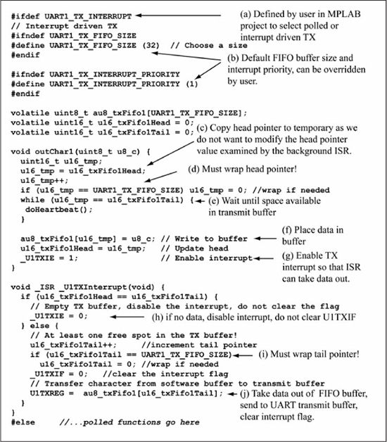
Next, the TX interrupt is enabled by setting _UTXIE (g). If an empty location exists in the UART TX transmit buffer as indicated by the U1TXIF flag being set, then an immediate jump is made to the TX ISR. Otherwise, the UART TX transmit buffer is full, so U1TXIF is cleared. In this case, the byte remains in the software TX FIFO until the current character in the TX shift register is finished transmitting and a byte is transferred from the UART TX transmit buffer to the TX shift register, freeing a location in the TX transmit buffer, setting the U1TXF flag, and causing a jump to the TX ISR.
The TX ISR (_U1TXInterrupt) first checks to see if data exists in the software FIFO by comparing the head index against the tail index. If the software FIFO is empty, the TX interrupt is disabled by clearing _UTXIE (h), but the U1TXIF flag is not cleared because it should remain set as long as an empty location exists in the TX transmit buffer. This is one of the few cases where an interrupt flag is not cleared before exit; instead, the interrupt is disabled so that the interrupt flag’s true condition does not immediately generate a jump back to the ISR after ISR exit. If data exists in the software FIFO then the tail index is incremented, wrapped if necessary (i), and the data from the software FIFO at au8_txFifo1[u16_txFifo1Head] is transferred to the UART TX buffer (j). In this condition, the U1TXIF flag is cleared before exit so that it can be set again once the currently transmitting character is finished.
Listing 10.1 shows the source code for the configUART1() function originally given in Figure 10.14 modified to include conditional compilation for interrupt-driven RX/TX. In the case of interrupt-driven RX, the _U1RXIF flag is cleared (_U1RXIF = 0) before the RX interrupt is enabled (_U1RXIE = 1). The _U1RXInterrupt ISR is triggered by arrival of RX data, and thus you need this interrupt enabled when the UART is configured. However, the code for interrupt driven TX only sets the interrupt priority, neither clearing the TX interrupt flag nor enabling the interrupt. This is because the TX interrupt flag is set when the UART is initialized and must remain set in order to trigger the _U1TXInterrupt ISR once a character is placed in the TX software FIFO by the outChar1() function, which enables the TX interrupt.
Listing 10.1: configUART1() Source Code
void configUART1(uint32_t u32_baudRate) {
  CONFIG_RP10_AS_DIG_PIN();             // RX RP pin must be digital
  CONFIG_U1RX_TO_RP(RB10_RP);           // U1RX <- RB10
  CONFIG_RP11_AS_DIG_PIN();             // TX RP pin must be digital
  CONFIG_U1TX_TO_RP(RB11_RP);           // U1TX -> RB11
  U1MODE = (0 << 15);                   // Clear existing errors before enable
  U1BRG = compute_brg(FCY, DEFAULT_BRGH1, u32_baudRate);  //config baudrate
  U1MODE = (1 << 15) | (DEFAULT_BRGH1 << 3);
  U1STA = (1 << 12) | (1 << 10) | (0 <<  1);
  DELAY_MS(1);                          // wait for 1 stop bit time
#ifdef UART1_RX_INTERRUPT
  _U1RXIF = 0;                          // Clear the flag

  _U1RXIP = UART1_RX_INTERRUPT_PRIORITY;       // Choose a priority
  _U1RXIE = 1;                                 // Enable the interrupt
#endif
#ifdef UART1_TX_INTERRUPT
  // Do not clear the U1TXIF flag!
  _U1RXIP = UART1_TX_INTERRUPT_PRIORITY;        // Choose a priority
  // Do not enable the interrupt until we try to write to the UART
#endif
}
Figure 10.21(a) summarizes reverse string application testing for different conditions, with the results for polled RX/TX and interrupt RX/polled TX previously given in Figure 10.19. Using both interrupt RX and interrupt TX helps in that it takes 34 strings to overflow the RX software FIFO instead of 14 for interrupt RX/polled TX. However, the eight buffer locations used by the interrupt TX software FIFO are better used if polled TX is done instead, with the interrupt RX software FIFO size increased from 8 to 16 as this requires 55 strings to overflow. Interrupt-driven TX costs more cycles per byte overhead in terms of processing time versus polled TX because bytes have to be first placed in the software TX buffer, then moved by the ISR to the hardware TX buffer. Thus, interrupt TX adds more processing overhead to the output stream, so these extra buffer slots are better used in the RX software FIFO. This illustrates that using an interrupt-driven approach for all I/O may not automatically be the best option; the trade-offs are application dependent. In a different application, interrupt TX might be attractive if output data occurred in bursts, the TX software FIFO was large enough to accommodate the largest burst, and the cycles spent waiting on a free spot in the TX HW buffer were needed for some other task. Figure 10.21(b) and Figure 10.21(c) summarize HW/SW FIFO usage for RX/TX serial data.
Figure 10.21
Reverse string testing, RX/TX FIFO usage summaries

The RS-232 Standard
The Electronic Industries Association standard EIA RS-232 defines signaling levels, external cabling, and handshaking protocols for asynchronous communication. RS-232 cabling uses either a 9-pin connector (DB9) or a 25-pin connector (DB25), with the DB9 typically used for personal computers. Figure 10.22 shows a minimal RS-232 PIC24 μC to PC asynchronous serial connection. The MAX 3232 RS-232 transceiver from Maxim [35] is only one of many different driver ICs that convert between RS-232 logic levels and CMOS logic levels. An RS-232 logic one has a range of –3 V to –25 V (–9 V typical) while an RS-232 logic zero has a range of +3 V to +25 V (+9 V typical).
Figure 10.22
Minimal RS-232 PIC24 μC to PC connection
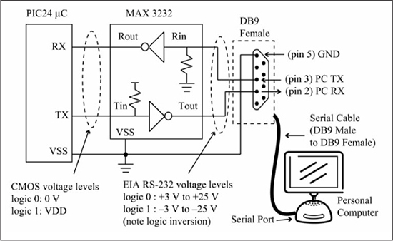
This is a minimal connection, for there are many other signals defined in the RS-232 standard that are used for external modem control and flow control. Because many PCs no longer contain a serial port, the usage of USB-to-serial converters has become popular. These adapter cables contain a microcontroller that communicates using the Universal Serial Bus (USB) with a host PC and converts USB packet data to asynchronous serial data. Some USB-to-serial converter cables use RS-232 levels, requiring the use of a level converter chip such as the MAX 3232. Other cables, such as the FTDI TTL-232R-3.3V cable used in the system startup schematic in Figure 8.3, conveniently output CMOS logic levels, allowing direct connection between the cable’s pins and the PIC24 μC. When using a USB-to-serial converter (or any RS-232 interface), you must know the signaling levels used by the cable’s pins, as RS-232 signaling levels will damage a PIC24 μC.
The minimal connection of Figure 10.22 has no method for either device to signal the other device about its ability to receive data; the sender assumes that the receiver is always able to accept new data. Two pins named CTS# (clear to send, pin 8 on the DB9) and RTS# (request to send, pin 7 on the DB9) can be used as handshaking lines to implement hardware flow control for serial data. The RTS# signal is a low-true output from the PC whose assertion indicates that the PC is ready to receive data. The CTS# signal is a low-true input to the PC, whose negation inhibits data transmission from the PC. These handshaking signals are included because the RS-232 standard was originally intended for communication between a terminal (data terminal equipment, or DTE) and a modem (data communication equipment, or DCE). In this historical model, the modem performed relatively low-speed communication over phone lines to a remote site. This means that the modem’s input buffer could become full, requiring it to tell the DTE (the PC) to stop sending data. On the PIC24 μC, the UxCTS# and UxRTS# pin functions shown in Figures 10.10 and 10.11 can be used to implement hardware flow control by connecting the PIC24 μC’s UxRTS# output to the PC’s CTS# input, and PC’s RTS# output to the PIC24 μC’s UxCTS# input. The PIC24 μC UxRTS# output is asserted when there is free space in the UART RX buffer, while negation of the UxCTS# input inhibits transmission from the UART. This provides flow control in both directions, from PIC24 μC to PC and vice versa. A full description of these pins and their usage is found in the PIC24 FRM [22]. For typical asynchronous communication speeds, hardware flow control is not required and thus this book does not use it. Sometimes a software flow control scheme using ASCII control codes XON (control-Q, 0x11) for “transmitter on” and XOFF (control-S, 0x13) for “transmitter off” is used when ASCII data is being exchanged. The advantage of software flow control is that no extra wires are needed; the disadvantage is that it cannot easily be used with arbitrary binary data since the codes 0x11 and 0x13 may be valid data bytes in the transmission. Some software flow schemes use a break character, which is defined on the PIC24 UART as a start bit + 12 zeros + stop bit, in conjunction with XON/XOFF codes for binary data software flow control. However, this depends on a UART’s capability for transmission and reception of break characters, and this may vary by UART implementation.
The Serial Peripheral Interface (SPI)
The Serial Peripheral Interface (SPI, pronounced as “spy”), originally developed by Motorola, is a three-wire synchronous serial link that has developed into a de facto standard due to its adoption by multiple semiconductor vendors. Figure 10.23 shows a SPI connection between a PIC24 μC and two peripheral devices. In this configuration, the PIC24 μC is termed the master as it starts every transmission by providing the clock (SCLK), with output data provided on the serial data out (SDO) pin and input data on the serial data in (SDI) pin. The two peripheral devices are termed slaves because they respond to SCLK pulses only if their low-true device select line (Device_Select#; the actual name used is device dependent) is asserted, which is handled using a PIO pin from the PIC24 μC. On each transfer, data is shifted out of the PIC24 μC via the SDO pin and shifted in from the selected slave device via the SDI pin. Thus, reading data from a slave device requires writing data, even if that data is simply dummy data. Similarly, data coming back from the slave during a write may only be dummy data, but it must be read and discarded to empty the SPI module input buffer.
Figure 10.23
PIC24 μC SPI connection to two slave devices
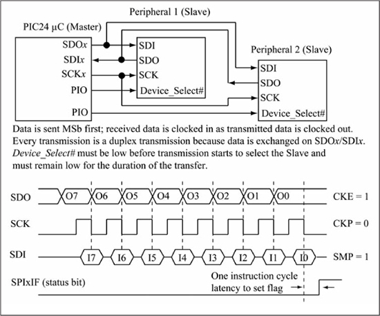
If the peripheral device is output only, then the SDI physical connection is not present, but garbage data is still clocked into the SPI input buffer on each transmission. Data is sent MSb first, and the clock polarity can be adjusted via a control bit named CKP, with value 0 if the idle state is low and 1 if the idle state is high. The edge that the output data is changed on is selected by the CKE control bit, with 0 used for an idle to active clock edge and 1 for an active to idle clock edge. There are four combinations possible using CKP/CKE; Figure 10.24 shows a waveform for CKE = 1, CKP = 0. The particular combination required is slave device dependent, but the CKE = 1, CKP = 0 choice is common. The SMP control bit determines if the input data is sampled in the middle of the output data (SMP = 0) or at the end of the output data (SMP = 1). Figure 10.23 shows the SMP = 1 case. An interrupt flag named SPIxIF is set whenever a transmission is completed. Transmissions from the PIC24 μC are selectable as either 8-bit or 16-bit. The 8-bit configuration is the most common option supported by SPI peripheral devices and is shown in Figure 10.23.
Figure 10.24 shows a block diagram of a SPIx module (as with the UARTx modules, there can be multiple SPI modules in a PIC24 μC, designated as SPI1, SPI2, and so on). In master mode, the PIC24 μC initiates the transmission, and if the PIC24 μC provides the SCKx it is generated from FCY with two cascaded prescalers, a secondary and a primary, as shown. The maximum allowable SCK frequency generated by a dsPIC33EP128GP502 is 10 MHz, so you must be careful to select prescaler values so that the generated SCK does not exceed this maximum. Each slave device also has its own maximum allowable SCK input frequency, which also must not be exceeded. The SSx# input is used when the SPI module in slave mode, that is, the PIC24 μC is acting as a SPI peripheral to another SPI master device. This operation mode is discussed later in this chapter. In master mode, a write to the SPIxBUF register is actually a write to the 8-entry transmit FIFO. Data in the transmit FIFO is immediately transferred to the SPIx shift register (SPIxSR) if it is idle. As data is shifted out of SPIxSR via the SDO pin, data is shifted into SPIxSR via the SDI pin. Once the transmission is complete, SPIxSR is transferred to the 8-entry receive FIFO. A read of the SPIxBUF register is actually a read of the receive FIFO. These transmit/receive FIFOs provide flexibility in transmitting and receiving values, as data can be dumped to the transmit FIFO and then the incoming data handled by an interrupt as it becomes available. The transmit/receive FIFOs are available when the SPI module is configured for enhanced buffer mode operation, which is only available on dsPIC33E/PIC24E devices. Legacy buffer mode is compatible with the older PIC24H/F families, and in this mode, the transmit/receive FIFOs are replaced by single registers named SPIxTXB (SPI transmit buffer) and SPIxRXB (SPI receive buffer). In legacy mode when SPIxRXB contains data, it is important to read SPIxBUF before another complete value is shifted into SPIxSR, or else a receive buffer overflow condition is generated, which halts operation of the SPIx module. In enhanced buffer mode, overflow occurs if a value in the SPIxSR register cannot be transferred to the receive FIFO because it is full. Enhanced buffer mode is selected by setting the LSb (named SPIBEN) of SPI Control Register 2 (SPIxCON2) to 1; the default value is 0 for legacy buffer mode.
Figure 10.24
SPIx module block diagram

Source: Figure redrawn by author from Figure 18.1 found in the dsPIC33E/PIC24E FRM SPI datasheet (DS7059C), Microchip Technology Inc.
Figure 10.25 shows the SPIxCON1 control register that contains the CKE, CKP, and SMP configuration bits as well as bits to select master/slave mode, 16-bit/8-bit mode, the secondary/primary prescaler values, and individual bits for disabling the SDOx, SCKx, and SSx pins if they are not used. There is a second control register named SPIxCON2 that supports a framed SPI protocol that this book does not discuss as most SPI peripherals do not use this protocol. As previously mentioned, the least significant bit of the SPIxCON2 register (named SPIBEN) is important as it selects either legacy buffer mode (SPIBEN = 0) or enhanced buffer mode (SPIBEN = 1) for the SPI transmit/receive buffers.
Figure 10.26 shows the SPIxSTAT status register and control register. The SPIEN bit enables the SPIx module when it is 1. The SPIROV status bit indicates if a receive buffer overflow condition has occurred; clearing this bit clears the overflow condition. The SPITBF and SPIRBF status bits, when set, indicate full conditions for the transmit buffer and receive buffer registers/FIFOs, respectively.
Figure 10.25
SPIxCON1: Control register 1

Source: Figure redrawn by author from Register 18.2 found in the dsPIC33E/PIC24E FRM SPI datasheet (DS70569C), Microchip Technology Inc.
These bits are automatically set and cleared in hardware by reading or writing the transmit and receive buffer registers/FIFOs.
Figure 10.26
SPIxSTAT: Status and control register

Source: Figure redrawn by author from Register 18.2 found in the dsPIC33E/PIC24E FRM SPI datasheet (DS70569C), Microchip Technology Inc.
Figure 10.27 shows waveforms for different combinations of CKE/CKP/SMP options. In the legacy buffer mode, the SPIx transmit buffer (SPIxTXB) in conjunction with the SPI shift register (SPIxSR) form a two-element FIFO. A new value can be written to an empty SPIxTXB while a transmission is in progress using SPIxSR. The SPIxIF interrupt flag is set whenever data is transferred from SPIxSR to SPIxRXB, indicating that a transmission has completed. Note that the SPITBF flag being 0 does not indicate a completed transmission; it only indicates an empty SPIxTXB register.
Figure 10.27
SPI master mode timing

Source: Figure redrawn by author from dsPIC33E/PIC24E FRM SPI datasheet (DS70569C), Figure 18-4, Microchip Technology Inc.
Listing 10.2 shows two C functions supporting SPI operation. The checkRxErrorSPI1() function checks for receive buffer overflow and calls reportError() with an appropriate message if an overflow is detected. The ioMasterSPI1(uint16_t u16_c) function first checks for receive buffer overflow using the checkRxErrorSPI1() function. A conditional compilation statement (line 11) checks for the existence of register bits _SRXMPT and _SPIBEN indicating a SPI module type with the enhanced buffer mode capability (lines 12-26) versus a SPI module type from an older CPU family (lines 28-33). Code lines 14-19 and 28-33 are the same and implement legacy buffer mode for both new and old SPI module types. The code for legacy buffer mode clears the SPI1IF flag, writes the u16_c parameter to the SPIx transmit buffer, and waits for the transmission to complete so that it can return the SPIx receive buffer contents. In enhanced buffer mode (lines 21-25), the SRXMPT flag from the SPI1STA register is used instead of the SPI1IF flag to check if the transmission has completed and received the datum available. The SRXMPT bit is a 1 if the Rx FIFO is empty. Either 8 or 16 bits are transmitted, depending on the configured mode of the SPI1 module. The remaining SPI examples in this chapter use legacy buffer mode as they do not require the extra flexibility offered by enhanced buffer mode.
Listing 10.2: ioMasterSPI1() C Function
1  void checkRxErrorSPI1(void) {
2   if (SPI1STATbits.SPIROV) {
3    // Clear the error
4    SPI1STATbits.SPIROV = 0;
5    reportError(“SPI1 Receive Overflow
”);
6   }
7  }
8
9  uint16_t ioMasterSPI1(uint16_t u16_c) {
10  checkRxErrorSPI1();
11 #if (defined(_SRXMPT) && defined(_SPIBEN))
12  // Enhanced SPI module, need to handle possibility of enhanced SPI mode
13  if (!SPI1CON2bits.SPIBEN) { // Check enhanced buffer mode bit
14   // Legacy mode
15   _SPI1IF = 0; //clear interrupt flag since we are about to write new value
16   SPI1BUF = u16_c;
17   while (!_SPI1IF) { //wait for operation to complete
18    doHeartbeat();
19   }
20  } else {
21   // Enhanced buffer mode
22   SPI1BUF = u16_c;
23   while (SPI1STATbits.SRXMPT) { // This flag is zero when RX buffer has data
24    doHeartbeat();

25   }
26  }
27 #else
28  // Legacy mode for older families (PIC24H/F, dsPIC33F)
29  _SPI1IF = 0; //clear interrupt flag since we are about to write new value
30  SPI1BUF = u16_c;
31  while (!_SPI1IF) { //wait for operation to complete
32   doHeartbeat();
33  }
34 #endif
35  return SPI1BUF;
36 }
37
SPI Example: The MCP41xxx Digital Potentiometer
Figure 10.28 shows an application of a Microchip MCP41xxx digital potentiometer [36] as a contrast control for the LCD module discussed in Chapter 8. A potentiometer is a device that provides a variable resistance. An analog potentiometer typically has three terminals; between two of the terminals the potentiometer’s full resistance is available (reference terminals PA0 and PB0 in Figure 10.28). The third terminal is called the wiper (terminal PW0 in Figure 10.28); this terminal provides a variable resistance when measured between the wiper and either one of the reference terminals. When the two reference terminals are connected to VDD and ground, changing the wiper setting varies the voltage on the wiper terminal between VDD and ground. An analog potentiometer’s wiper setting is changed via some mechanical interface such as turning a shaft. A digital potentiometer’s wiper setting is changed using a parallel or serial interface, with serial interfaces being the most common. In the dsPIC33E/PIC24E device family, the SPI1 interface pins are assigned fixed pin locations on a given target device for higher speed operation than the SPI2 interface pins, which can use remappable pins at the cost of a slightly lower maximum SPI clock speed. On the dsPIC33EP128GP502 reference system, the SPI interface pins SDO1 and SCK1 are fixed at the same physical pin locations as pins RB8 and RB7, respectively. Pin RB2 is used as the potentiometer chip select, which is an arbitrary selection since any PIO pin could be used for this function.
The MCP41xxx digital potentiometer comes in 10 kΩ (MCP41010), 50 kΩ (MCP41050), and 100 kΩ (MCP41100) configurations and uses a SPI port for setting the 8-bit wiper register for the potentiometer. The supported VDD range is 2.7 V to 5.5 V. In the configuration shown in Figure 10.28, a wiper value of 255 sets the PW0 output voltage to approximately 255/256 × VDD, while a value of 0 sets the PW0 output voltage to ground. The wiper register is set to 128 (midway) on power-up. Higher potentiometer values reduce the static current that is drawn by the potentiometer when it is active. For example, a 50 k potentiometer with VDD = 3.3 V draws 3.3 V/50 kΩ = 66.7 μA static current through the potentiometer resistance, while a 100 kΩ potentiometer reduces this current by 50% to 33.3 μA.
Figure 10.28
PIC24 μC to MCP41xxx digital potentiometer interface

Figure 10.29 shows the command protocol for the MCP41xxx. Each transaction consists of two bytes, a command byte and a data byte. The CS# (chip select) input must be brought low to enable the device before any data is sent and brought high after transmission is finished in order to execute the command. The wiper register is set by the command byte 0x11 followed by the wiper register value. The shutdown command opens (disconnects) the potentiometer by opening the PA0 terminal and shorting the PW0 and PB terminals. This reduces total static current draw of the MCP41xxx to less than 1 μA. The data byte for the shutdown command is ignored but it still must be sent for the command to be recognized. If MCP41xxx shutdown mode were to be used with the LCD application of Figure 10.29, then you would want to reverse the PA0 and PB0 connections so that VL of the LCD is shorted to VDD during shutdown, blanking the display. This would mean that a wiper code of 255 sets the PW0 voltage to near ground, while a code of 0 sets the PW0 voltage to VDD.
Figure 10.29
MCP41xxx command protocol
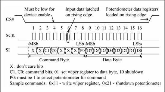
Figure 10.30 gives code for testing the PIC24 μC to MCP41xxx interface. The while (1) loop of main() prompts the user for an 8-bit value and sends this as the wiper register value to the MCP41xxx via the setPotWiper(uint8_t u8_i) function. The ioMasterSPI1() function of Listing 10.2 is used to send the 0x11 command byte, followed by the wiper register value. Observe the potentiometer chip select is asserted by the SLAVE_ENABLE() macro and negated by SLAVE_DISABLE(), and that the chip select is enabled for both byte transmissions. Within the while (1) loop of main(), the <stdio.h> library function sscanf is used to parse a decimal number from the input string, and the <stdio.h> library function printf is used for printing this value back out in decimal format. See a C standard library reference for more information on using these functions; these examples use these functions for convenience purposes when formatted character I/O is required. The configSP1() function configures the SPI1 module for CKP = 0, CKE = 1, 8-bit mode, master mode, and a clock prescaler value of 1:6. This means that the SPI clock frequency is then FCY/(1×6). Since the internal FCY is 60 MHz for the dsPIC33EP128GP502 reference system, this gives an SCK frequency of 60 MHz/6 = 10 MHz, which is the maximum allowed for the dsPIC33EP128GP502 SPI1 port for duplex operation. The 10 MHz SCK frequency also happens to be the maximum allowed for the MCP41xxx according to its datasheet. This maximum clock frequency is used for example purposes as SPI bus speed is typically not an important factor for a digital potentiometer; thus you may want to use an SCLK speed that is less than the maximum for timing margin purposes. The configSPI1() function also configures the PIO pin used for MCP41xxx chip select, negates the MCP41xxx chip select and enables the SPI1 module. The macros used for configuring the SPI1CON1 register are defined in libinclude pic24_spi.h. Bits that are not included in the SPI1CON1 configuration statement use the default values from Figure 10.25 after reset.
Figure 10.30
Test code for PIC24 μC to MCP41xxx interface

SPI Example: PIC24 μC Master to DS1722 Thermometer
Figure 10.31 shows a PIC24 μC connected to a Maxim DS1722 digital thermometer [37] using a SPI port. The DS1722 has a high-true chip enable (CE) and can be configured for either a SPI operation (SERMODE = high) or for a generic three-wire serial interface (SERMODE = low). The VDDD and VDDA pins are digital supply and analog supply, respectively, and are tied to 3.3 V in this application. The DS1722 senses ambient temperature, which can be read as a digital value via the SPI port.
Figure 10.31
PIC24 μC SPI master to DS1722 connection

Operational details for the DS1722 are given in Figure 10.32. The DS1722’s 8-bit configuration register determines the conversion mode and precision; see Figure 10.32(a). The two conversion modes are either continuous conversion (SD = 0) or one-shot mode (SD = 1). In one-shot mode, the DS1722 starts a conversion when a 1 is written to the 1SHOT bit. When the conversion is finished, the 1SHOT bit is cleared and a power-down state is entered. The temperature value converted to Celsius is available in two 8-bit registers that form an 8.4 two’s complement fixed point value (see Chapter 7), with the MSB containing the integer portion and the upper four bits of the LSB containing the fractional portion. Bits R2/R1/R0 of the configuration register control the conversion precision as shown, with longer conversion times required for higher precision. The resulting 16-bit temperature value can be converted to a floating-point Celsius value by dividing it by 256 because the 12-bit value is returned in the upper 12 bits of the 16-bit word. Internal registers on the DS1722 are accessed by first writing an address byte followed by reading or writing data bytes at that address.

The address byte written determines if the next byte is a read or write. For example, to write the configuration register, write two bytes with the first being 0x80 (the address byte) followed by a byte that sets the configuration register. To read the configuration register, again write two bytes with the first being 0x00 (the address byte) followed by a dummy byte (any value works). The byte returned by the DS1722 for the written dummy byte is the current configuration value. Figure 10.32(b) shows the SPI transfer required for writing to the configuration register. The two temperature registers can be read in one SPI operation by writing an address of 0x01 followed by a write of two dummy bytes; the data returned by the dummy byte writes are the LSB and MSB of the temperature, as shown in Figure 10.32(c). Reading the temperature registers does not disturb the current conversion. Note that the temperature registers are read-only.
Code for configuring the SPI port, writing a configuration byte, and reading the 16-bit temperature is shown in Figure 10.33. The DS1722 can use either clock polarity, but requires data changes on the inactive-to-active clock edge (CKE = 0). The writeConfigDS1722(uint8_t u8_i) function writes u8_i to the DS1722 configuration register. The readTempDS1722() function reads the two 8-bit temperature registers and returns them as a signed 16-bit value (int16_t).
Figure 10.33
C code for reading/writing DS1722 registers

The main() code for testing the DS1722 is shown in Figure 10.34(a). The writeConfigDS122(0xE8) function call configures the DS1722 for continuous conversion and 12-bit precision. The while (1) loop delays for 1.5 seconds then reads the 16-bit temperature and converts it to both Celsius (f_tempC) and Farenheit (f_tempF) floating-point values. The printf statement is used for formatted output of these values to the console. Figure 10.34(b) shows typical output during operation; the temperature values increased when a finger was placed on the DS1722, and then it decreased once it was removed.
Figure 10.34
C code for testing the DS1722

SPI Example: PIC24 μC Master to PIC24 μC Slave
A PIC24 μC can also act as SPI slave peripheral, which can be useful in a multi-CPU application or if a PIC24-based product requires an external SPI port. Figure 10.35(a) shows a PIC24 μC SPI master to PIC24 μC SPI slave connection that is used to illustrate this operation mode. The application is the string reversal application previously used to illustrate interrupt-driven UART TX/RX operation.
Figure 10.35(b) illustrates the master/slave I/O actions in this application. An input string arrives at the master via the UART, which is then sent to the slave via the SPI port. The slave reverses the string then notifies the master that data is ready by asserting an output ready signal, which is implemented using RB2 in Figure 10.35. This use of a PIO pin to coordinate data transfer between two devices is known as handshaking. The master then reads the reversed string from the slave using the SPI and the slave negates its output ready signal. The process repeats when another string arrives at the master. PIO RB3 is used on the master to assert the slave select (SS1#) input on the slave.
Figure 10.35
PIC24 μC SPI master to PIC24 μC SPI slave connection
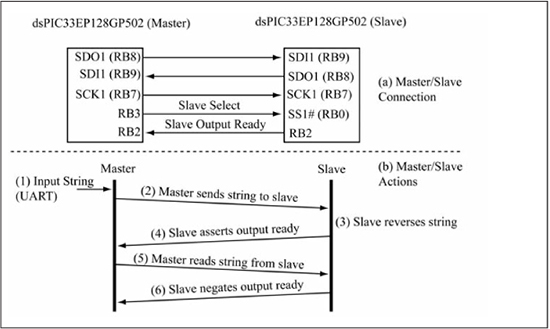
Figure 10.36 shows the SPI configuration code for both the master and slave applications. The master’s configSPI1() function is the same as used in Figure 10.30 with the addition of CONFIG_SLAVE_ORDY(), which configures RB2 as a digital input to handle the slave’s output ready handshaking signal. The slave’s configSPI1() function is quite different as the SPICON1 register is configured for slave mode with the SS# input enabled. Because the master supplies SCK1, there is no need for the slave to configure the SCK1 prescalers. Also, the slave application uses interrupt-driven I/O for SPI transfers, so the SPI1 interrupt is enabled. Both slave and master used CKE = 0 (SPI_CKE_OFF) and CKP = 0 (CLK_POL_ACTIVE_HIGH) which was arbitrarily chosen for this example. It is important that both master and slave use the same settings for data format consistency. The dsPIC33E/PIC24E Family Reference Manual for the SPI module notes that when CKE = 1, the SS1# pin must be enabled in slave mode to meet timing requirements. This example uses CKE = 0, so use of the SS1# pin is optional but was included in this code for demonstration purposes.
Figure 10.36
SPI master, slave configuration

Figure 10.37 shows the master code for the string reversal application. The main() function uses a two-state FSM. In state STATE_GET_IN_STRING, a string is read from the console, then sent to the slave using the sendStringSPI1() function. The ioMasterSPI() function discussed previously is used to send each byte to the slave. The STATE_GET_REV_STRING state waits for the slave to assert the output ready signal, then uses the getStringSPI1() to read the reversed string from the slave. Observe that the master must transmit a byte to the slave in order to get a byte back from the slave. When the master receives a null byte from the slave, then it knows that the end of the string has been reached.
Figure 10.38 shows the slave code for the string reversal application. All of the work is done within the _SPI1Interrupt ISR, which is triggered each time a byte arrives at the slave and uses a three-state FSM. The STATE_WAIT_FOR_STRING is used for receiving the string to be reversed from the master; the input string is written to the sz_1 buffer. When a complete string is received, the previously discussed reverseString() function does the string reversal. Then, the first character of the reversed string is placed into SPIBUF before asserting the output ready and transitioning to state STATE_SEND_REV_STRING. In slave mode, writing to the SPIBUF does not transmit the character; the data is held in the SPI shift register until the master provides the SPICLK pulses for the next transmission. The STATE_SEND_REV_STRING state writes a character of the reversed string to the SPIBUF so that it can be read by the master and transitions to the STATE_LAST_REVCHAR_STRING state when the null terminator is written. When STATE_LAST_REVCHAR_STRING is triggered, this means the master has read the null terminator of the reversed string, so output ready is negated and the slave transitions back to the STATE_WAIT_FOR_STRING to wait for the next input string.
Figure 10.37
Master C code for string reversal application

Figure 10.38
Slave C code for string reversal application

Figure 10.39 shows a logic analyzer screenshot of the SPI bus activity for the reverse string application using the two character string “MS”. The SDI1 and SDO1 labels are from the master’s perspective; Figure 10.39(a) shows the “MS” string being transmitted to the slave, while Figure 10.39(b) shows the master reading the reversed string from the slave.
Figure 10.39
Logic analyzer trace for string reversal application

The advantage of the SPI bus lies in its simplicity and its high data rate transfer. Many peripheral ICs that provide connectivity to block-oriented interfaces such as Ethernet, memory cards, and USB have a SPI port as their μC interface. However, the fact that SDI is linked to SDO with the master having to initiate all data exchanges limits flexibility. For CPU-to-CPU communication, an asynchronous serial interface is typically a better choice if high data rates are not required since the TX/RX channels are independent.
The I2C Bus
The Inter IC (I2C) bus [38] was introduced by Philips Semiconductor in the early 1980s and it has since become a de facto standard serial bus. The term bus in this context is a formal designation and is different from the previous casual usage of “bus” to describe groups of parallel wires. In this context, a bus is a communication channel in which there are one or more transmitters and multiple receivers. All receivers see data that is transmitted over the communication channel. Each receiver decodes transmitted messages and uses an address within the message to determine if it is the target of the message. The receiver that is the message target then replies back to the message transmitter over the same communication channel. Figure 10.40 gives two examples of bus communication channels. Figure 10.40(a) shows how normal conversation among a group of friends is essentially bus-based communication as the transmitter uses the name of the person as the address when sending a message across the communication channel, which is air. The person who is addressed by name then responds to the transmitter. Figure 10.40(b) illustrates how Internet addresses are used on an Ethernet network for computer communication. An Ethernet network is a bus, as all computers monitor traffic on the network and only respond to those data packets whose header addresses match their assigned Internet address (note: technically, MAC addresses are used by the hardware interface on the receiving computer for packet reception, but Internet addresses are shown in Figure 10.40 for simplicity since those are more familiar).
Figure 10.40
Two examples of bus communication

I2C Physical Signaling
Figure 10.41 shows an I2C bus, which consists of a data line (SCL) and a clock line (SDA) used to implement half-duplex communication. Observe that the devices connected to the I2C bus do not have chip select signals like SPI-based peripherals. Instead, each device has a 7-bit address whose upper 4 bits (n3n2n1n0) shown in Figure 10.41 are device specific and encoded within the device. The next 3 bits (A2, A1, and A0) of the 7-bit address are typically determined by external pins that are connected to either VDD or ground to provide logic 1 or logic 0, respectively. The address is always sent as the first byte of an I2C bus transaction that transfers a group of bytes, which is initiated by the bus master (details of transactions are given later in this section). Each I2C peripheral device decodes the address byte to determine if it is the target of the transmission, removing the need for individual chip select lines. Adding another I2C device to the bus does not require using an additional pin on the PIC24 μC, a distinct advantage over SPI-based peripherals. Like the SPI protocol, the PIC24 μC can act as either a slave or master on the I2C bus; the examples in this chapter always use the PIC24 μC as the sole I2C bus master (see Chapter 13 for an example of PIC24 I2C slave operation). The pull-up resistors on the SCL/SDA lines are needed because these drivers are open-drain in order to provide multi-master capability. In a multi-master bus, any device can act as a bus master. This requires an arbitration mechanism that decides which device controls the bus in the case of simultaneous attempts to access the bus (see Chapter 13 for a discussion of I2C bus arbitration). The most recent version of the I2C specification has support for a 10-bit address that is transmitted in the first two bytes of a transaction. The I2C peripherals used within this book’s examples use 7-bit addresses.

Figure 10.42 shows the details of one byte of an I2C bus transfer. The idle condition occurs when both the SDA and SCL lines are high prior to the beginning of a bus transfer.

The master always provides the SCL signal and initiates an I2C transaction. The start condition, a high-to-low transition on SDA while SCL is high, signals the beginning of an I2C data transfer. The first byte after a start condition is always the address byte used to select a particular I2C peripheral. Multiple bytes can then be sent within an I2C transaction with each byte sent MSb first. SDA data is stable while SCL is high and changes while SCL is low. Each byte transmission ends with a 9th bit time in which the transmitter stops driving the SDA line so that the receiver can acknowledge the byte transmission by pulling the SDA line low. If the receiver does not drive SDA low, the SDA pull-up resistor keeps SDA high and the transmitter reads a 1 for the acknowledgement bit instead of a 0. A 1 acknowledgment bit is called a not-acknowledge, or a NAK, while a 0 acknowledgment bit is called an ACK. Typically, the transmitter will interpret this as an error condition and abort the transfer. There are multiple reasons why a receiver may not acknowledge a byte transmission; if this is the address byte, a coding mistake could result in the wrong address being used, or perhaps the receiver cannot accept new data or has experienced an internal failure. In any case, the acknowledge bit provides feedback to the transmitter on whether a byte has been received. The acknowledgment bit is non-optional for normal transfers because each byte transmission includes the overhead of an acknowledgment bit. The master provides the acknowledgment bit when a slave sends a byte to the master during a read operation. After an acknowledgment bit, a slave can hold the SCL line low, which forces the master into a wait condition until the slave releases the SCL line.
In this way, the slave can provide flow control on a byte-by-byte basis; this is the only time that the slave may drive the SCL line. The stop condition, defined as a low-to-high SDA transition while SCL is high, ends an I2C transaction and frees the bus, allowing it to be driven by another bus master. After the stop condition, both SCL and SDA are undriven and thus pulled high by the pull-up resistors. A repeated start condition is when another start is sent within a transaction; this ends the current transaction and begins a new transaction, thus allowing the current bus master to start a new transaction without relinquishing control of the bus. For a single I2C bus master like most of the examples in this book, a repeated start can be replaced by a stop followed by a start if this is more convenient from a coding viewpoint. More details on special transactions such as CBUS transfers in which acknowledgment bits are not provided are found in the I2C specification [38].
I2C Transactions
As previously mentioned, bytes are transferred between the I2C master and slave in a transaction, which can either be a write transaction or a read transaction. Figure 10.43 shows the general form of write and read transactions. The first byte in either a read or write transaction is always sent by the master, with the upper 7 bits containing the 7-bit I2C address. The least significant bit of this byte indicates the direction of the transfer. A 0 signifies a write operation (transfer from master to slave), while a 1 specifies a read (transfer from slave to master). In a write transaction—Figure 10.43(a)—all of the bytes are sent by the master, with the slave providing all of the ACK bits. In a read transaction—Figure 10.43(b)—the master provides the first byte with the slave providing the ACK bit, and then the slave sends the remaining bytes with the master providing the ACK bits for these bytes. The last byte read by the master is acknowledged with a NAK bit (logic value = 1) to signal to the slave device that it should not send another byte. Figure 10.43(c) shows a write transaction followed by a read transaction, with a repeated start condition used between the two transactions. As previously mentioned, if it is known that there is only one device on the I2C bus that will function as a master, then the repeated start can be replaced by a stop condition followed by a start condition as there is no danger of another master grabbing the bus after the write transaction concludes.
Sample Question: An I2C transaction is the sequence of bytes: 0xA4, 0x30, 0xAD, 0x4C. Is this a read or write transaction? What is the 7-bit address of the slave device? How many data bytes are transferred in this transaction?
Answer: The LSb of the first byte (0xA4 = 0b10100100) determines the transaction type. It is a 0, so this is a write transaction. The upper 7 bits of the first byte specify the address of the slave device and these bits are 0b1010010, which is 0x52 in hex. The three remaining bytes (0x30, 0xAD, 0x4C) are data bytes transferred from the master to the slave.
Figure 10.43
I2C write and read transactions

Library Functions for I2C Transactions
Figure 10.44(a) summarizes the I2C library functions supplied with this book for supporting I2C basic operations such as module configuration, performing a start/rstart/stop operation, sending one byte, and receiving one byte. These basic functions are used by the functions listed in Figure 10.44(b) that accomplish complete I2C transactions that read or write one or more bytes to an I2C slave peripheral. The implementation of these functions is discussed in the next section. The 1 at the end of each function name indicates that these functions work with I2C module 1 on the target device; dsPIC33E/PIC24E devices can have more than one I2C module depending on the device.
Figure 10.44
I2C support function summary

Figure 10.45 shows a write transaction that writes the bytes 0x3C and 0xD8 to a slave device with a 7-bit address of 0x54. Figure 10.45(a) shows the transaction implemented using the operation functions from Figure 10.44(a). This code uses the putI2C1 function to write the bytes to the slave device. The putI2C1 function executes a software reset if a NAK bit is returned by the slave device since this typically indicates a non-responsive slave device. Alternatively, the putNoAckCheckI2C1 function could be used as it returns the received ACK bit instead of doing a software reset on NAK, which allows the user to determine the action to be taken on a NAK. Note that the first putI2C1 function uses an argument of 0x54<<1, which places the 7-bit address into the upper-most 7-bits of the argument and shifts a 0 into the lower bit to indicate a write transaction as per Figure 10.43(a).
This means that the actual byte written is 0xA8. Figure 10.45(b) implements the write transaction using the transaction functions of Figure 10.44(b), which means that the code of Figure 10.45(a) can be replaced by a single function call. The first argument to all of the transaction functions is the first byte written by the master, with the lower bit of this byte cleared or set within the function depending on if it is a write or read transaction. The remaining arguments for the transaction functions deal with the data to be transferred to or from the slave device. The write1I2C1/write2I2C1 transaction functions send a fixed number of data bytes (1 and 2, respectively), while the writeNI2C1 function sends a variable number of data bytes. The transaction functions are shortcuts for common groupings of the primitive I2C operations.
Figure 10.45
I2C write transaction code example

An I2C transaction that reads two bytes from a slave device with a 7-bit address of 0x54 is given in Figure 10.46. Code using I2C operation functions is shown in Figure 10.46(a). The first byte sent to the slave using the putI2C1 function is the same as in Figure 10.45(a), except that the lower bit is set to a 1 by a bitwise OR operation to indicate a read transaction. The actual byte sent is (0x54<<1) | 0x01 = 0xA9. The remaining function calls use the getI2C1 function to return the bytes from the slave device, with the argument to getI1C1 being the ACK bit value to return to the slave. The returned ACK bit values should be 0 (ACK) except for the last byte read that must return a 1 (NAK) as per Figure 10.43(b), so getI2C1(1) is used for the last byte instead of getI2C1(0). Figure 10.46(b) uses a single read2IC1 transaction function to implement the code of Figure 10.46(a); observe that the addresses of the variables used for storing the returned bytes are passed to the function. The read1I2C1/read2I2C1 transaction functions read a fixed number of data bytes (1 and 2, respectively), while the readNI2C1 function reads a variable number of data bytes.
Figure 10.46
I2C read transaction code example

Before using an I2C module on the PIC24, it must be initialized using the configI2C1 function from Figure 10.44(a). The parameter for this function specifies the desired I2C bus frequency in kHz, with standard frequencies of 100 kHz, 400 kHz and 1000 kHz supported by most devices and by the reference dsPIC33EP128GP502 system of Chapter 8. In practice, an I2C device will work with any bus frequency less than its device-specific maximum frequency.
I2C on the PIC24 μC
This section discusses the specific implementation of the functions of Figure 10.44 in the PIC24E family (there are no major differences between I2C implementations on the PIC24E/H/F and dsPIC33E/F families). The PIC24 I2C module registers and commonly used control and status bits are summarized in Figure 10.47 (complete information on the status and control register bits are found in the I2C section [24] of the dsPIC33E/dsPIC24E Family Reference Manual). There are two I2C modules available on the reference dsPIC33EP128GP502 system in Chapter 8. The SCLx/SDAx pins on a PIC24 μC are assigned to fixed pin locations and not to remappable pins like the SPI and UART pin functions because of the specialized signaling requirements of the I2C interface. Each PIC24 μC has an alternate set of I2C pins named ASCLx/ASDAx that can be selected via a configuration bit; the choice is invisible to user application code. On the reference dsPIC33EP128GP502 system in Chapter 8, only the alternate set of I2C pins are available on the 28-pin physical package, with ASCL1/ASDA1 mapped to physical pins 17/18 and ASCL2/ASDA2 to physical pins 15/16 (see the pinout diagram in Figure 8.2). The code examples in this chapter use module 1.
Figure 10.47
PIC24 I2C registers

The I2C clock speed (FSCL) is controlled by a 9-bit baud rate register (I2CxBRG) whose value is calculated by Equation 10.4, which is valid for the dsPIC33E/PIC24E family; the PIC24H/F family subtracts FCY/10,000,000 from this value:
The dsPIC33E/PIC24E Family Reference Manual defines an additional correction factor for Equation 10.4 called Pulse_Gobbler_Delay, which we ignore since it is small and device specific. The dsPIC33EP128GP502 datasheet provides timing specifications for the standard clock rates of 100 kHz, 400 kHz, and 1 MHz.
The C source code for the configI2C1(uint16_t u16_FkHZ) function in Figure 10.48 computes and initializes the I2C1BRG register value for operation at u16_FkHz kHz clock frequency and enables the module by setting the I2CEN bit (I2C1CON<15>). This enables the module for both master and slave operation, unlike the SPI module that must be explicitly configured for either master or slave operation. The I2C examples in this chapter use the PIC24 μC as a single bus master; see Chapter 13 for an example of I2C slave mode operation. The startI2C1() function (see Figure 10.48) initiates the start condition by setting the SEN bit; the ensuing while (I2C1CONbits.SEN) loop is exited when the hardware clears the SEN bit on completion of the start operation. The startI2C1() function uses the watchdog timer to escape the infinite wait loop in the unlikely event of hardware malfunction. The rstartI2C1() and stopI2C1() functions are similar, except they use the RSEN and PEN bits, respectively.
Figure 10.48
C source code for configI2C1() and startI2C1() functions
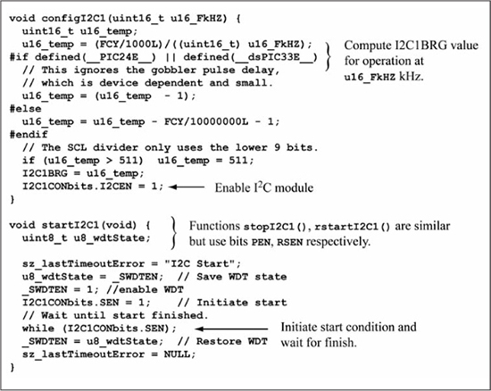
Transmitting a single byte on the I2C bus is accomplished by the putI2C1(uint8_t u8_val) function, whose source code is shown in Figure 10.49. The u8_val byte to be transmitted is written to the I2C transmit register (I2C1TRN). This sets the TRSTAT status bit, which is cleared by the hardware when the 8-bit value has been transmitted and an acknowledgement bit received from the slave. The acknowledgement bit value (0 for ACK, 1 for NAK) is available in the ACKSTAT bit, and the putI2C1() function calls reportError() with an appropriate error message if a NAK is returned.
The putNoAckCheckI2C1(uint8_t u8_val) function listed in Figure 10.44 also transmits a single byte, but it returns the value of the ACKSTAT bit instead of reporting an error on a NAK condition, because slave peripherals sometimes use the acknowledgement bit for returning status information. The getI2C1(uint8_t u8_ack2Send) function whose source code is given in Figure 10.49 reads a single byte from the I2C bus then writes an acknowledgement bit (u8_ack2Send). Receive is enabled by setting RCEN bit, which is cleared by the hardware on reception of the 8th bit into the I2C input shift register. The receive buffer full (RBF) status bit is set when the 8-bit value is transferred into the receive register (I2C1RCV) and is cleared when this register is read. After reading the I2C1RCV register, the acknowledgement bit is sent back by setting the ACKDT bit to the acknowledgement bit value to be transmitted (u8_ack2Send). The acknowledgement bit transmission is initiated by setting the ACKEN bit, which is cleared by the hardware when the acknowledgement operation is finished. The value read from the receive register is the return value of the getI2C1() function.
Figure 10.49
C source code for putI2C1() and getI2C1() functions

Figure 10.50 shows the C source code for the I2C read/write transaction functions of Figure 10.44(b). These functions are provided for convenience purposes and are used in the I2C interfacing examples that follow this section. The writeNI2C1() and readNI2C1() functions are useful for transferring a block of data to or from a slave peripheral. The I2C_RADDR(x) and I2C_WADDR(x) macros are used for clearing and setting the R/W# bit of the I2C address byte (u8_addr) parameter passed to the read/write transaction functions.
Figure 10.50
C source code for I2C read/write transaction functions
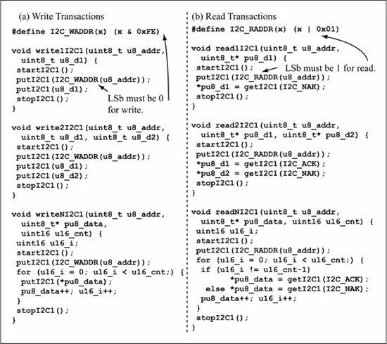
I2C Example: PIC24 μC Master to DS1631 Thermometer
The first I2C interfacing example is a PIC24 μC master to Maxim DS1631 Digital thermometer/thermostat [39] slave, as shown in Figure 10.51. The DS1631 is similar in many ways to the previously discussed DS1722 digital thermometer, but differs in that it supports 9- to 12-bit precision but not the 8-bit precision also supported by the DS1722. The DS1631 also has a thermostat function in which the TOUT pin goes high when the temperature exceeds a user-programmable high temperature trigger that is stored in a non-volatile 16-bit register named TH. The TOUT pin returns low once the temperature falls below a user-programmable low temperature trigger that is stored in a non-volatile 16-bit register named TL.
Figure 10.51
PIC24 μC I2C master to DS1631 digital thermometer connection

Figure 10.52 details the commands supported by the DS1631. The standalone command (a) is used to start and stop continuous conversions. The 8-bit write (b) and read (d) commands are used to access the 8-bit registers, such as the configuration register. The 16-bit write (c) and read (d) commands are used for the 16-bit registers, which are the temperature register (read-only) and the TH, TL registers. Observe that a read command consists of two separate I2C transactions; an I2C write transaction that sends the command byte to the DS1631 followed by an I2C read transaction that returns the data.
The DS1631 configuration register details are shown in Figure 10.53. The 1SHOT and continuous conversion modes work similarly to the DS1722, except that continuous conversion mode must be explicitly begun via the standalone command shown in Figure 10.52 (the DS1631A version begins conversions immediately on power-up). If the device is configured for one-shot mode, then the standalone command (0x51) initiates a conversion.
Figure 10.52
DS1631 I2C operation

Figure 10.53
DS1631 configuration register
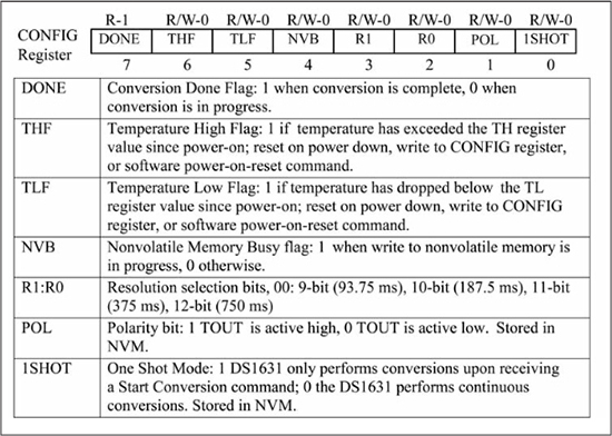
Code for testing the DS1631 interface is given in Figure 10.54. The I2C transaction functions previously discussed in Figure 10.44(b) are used to implement the DS1631 commands of Figure 10.54 in the functions writeConfigDS1631(), startConversionDS1631(), and readTempDS1631(). The slave address passed to the I2C transaction functions is 0x90, which corresponds to A2/A1/A0 pins of the DS1631 all tied low, as shown in Figure 10.53. The main() code configures the I2C module for 400 kHz operation, then configures the DS1631 for continuous conversion and starts the conversions. The while (1) loop code is essentially the same code as used for the DS1722 of Figure 10.34 in that the 16-bit temperature is read after a delay, then printed to the console in hex, degrees Celsius, and degrees Fahrenheit.
I2C bus activity captured during the readTempDS1631() function is shown in Figure 10.55. The write1I2C1() function call performs a one-byte write transaction that writes the READ_TEMP (0xAA) command to the DS1631. This is followed by the read2I2C1() function call that reads two bytes from the DS1631. Observe that the DS1631 address during the write transaction is 0x90, while during the read transaction it is 0x91, with the difference being the LSb value (0 for write, 1 for read). The 16-bit temperature read is 0x1D30, which is 0x1D30/256 = 7472/256 = 29.1875°C.
Figure 10.54
Code for testing the DS1631
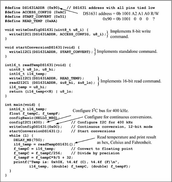
Figure 10.55
I2C bus activity during DS1631 operation

I2C Example: PIC24 μC Master to 24LC515 Serial EEPROM
The 24LC515 512K serial EEPROM [40] has an internal organization of 64 Ki x 8 and uses an I2C port for communication. Figure 10.56 shows a PIC24 μC master to 24LC515 connection. The write protect (WP) pin on the 24LC515 can be used to disable writes to the device; it can be left open or tied to VSS to enable writes. The A2 input is an unused input that must be tied high for the device to function correctly. The A1 and A0 inputs are used to personalize the device address by connecting them to either VDD or ground. This allows up to four 24LC515 devices to exist on the same I2C bus.
Figure 10.56
PIC24 μC master to 24LC515 serial EEPROM connection

Figure 10.57(a) shows the address byte format for the 24LC515. The upper 4 bits are fixed at 1010. The 64 Ki x 8 organization of the 24LC515 means that addresses are 16 bits with a range of 0x0000 to 0xFFFF. However, the internal organization of the 64 Ki x 8 memory is split into two 32 Ki memory blocks, each with its own internal 15-bit address counter. The B (block select) bit of the I2C address byte determines whether the current operation is to the low memory block (0x0000 through 0x7FFF) or high memory block (0x8000 through 0xFFFF). Thus, it is best to view the 24LC515 as two separate 32 Ki x 8 memories that are selected by the B bit in the I2C address byte. The least significant bit of the address byte is the R/W# bit as with all I2C address bytes. The write operation format for the 24LC515 is given in Figure 10.57(b). The I2C address byte is followed by the high and low address bytes of the starting location for the write. The most significant bit of the high address byte is a “don’t care” as the block select bit within the I2C address byte determines which memory block is being written; these 15 address bits are written to the internal address counter for the 32 Ki block selected by the block select bit of the address byte. The internal page size of the 24LC515 is 64 bytes, so up to 64 bytes can be written in one write operation. The incoming bytes are placed into an internal 64-byte buffer using the lower 6 bits of the address, while the remaining upper bits specify the page that is written. The starting address of a 64-byte page has its last six bits as all zeros.
If the write command address does not begin on a 64-byte boundary, bytes wrap to the beginning of the page once the internal address counter increments past the page boundary. Because of this, the best practice is to write a complete page at one time and force the starting address to begin on a page address. The actual write to EEPROM begins when a stop condition is received, with worst-case write completion time specified as 5 ms. However, the end-of-write condition can be polled by sending the write command and checking the ACK bit status, as shown in Figure 10.57(c). If the acknowledgement bit returns as 1 (a NAK), a write is still in progress. Once the acknowledgement bit returns as 0, the next operation can be started. It is more efficient to poll for end-of-write at the beginning of a write operation than to place a delay of 5 ms after each write operation. Experimental results showed that writes typically required about 3.1 ms, which is considerably shorter than the 5 ms worst-case specification.
Figure 10.57
LC515 I2C address format and write operation

Figure 10.58 shows read operation sequencing for the 24LC515. A sequential read—Figure 10.58(a)—returns the memory contents pointed to by the internal address counter of the 24LC515. Each data byte returned by the 24LC515 increments the internal address counter for the selected block. An acknowledgment bit of 0 returned by the PIC24 μC causes the 24LC515 to output another data byte. An acknowledgement bit of 1 returned by the PIC24 μC causes the 24LC515 to release the SDA line and to stop sending data. A sequential read can access the contents of one entire 32 KiB memory block, either high or low, as determined by the block select bit sent in the I2C address byte at the beginning of the read transaction. When the internal address counter reaches the end of a 32 Ki block, it wraps around to the beginning of the block. Figure 10.58(b) shows how to use the write command to set the internal address counter before beginning a sequential read. Sending a repeated start condition (or a stop followed by a start) after the EEPROM address bytes halts the write command. Only the internal address counter is affected by the write operation; an internal write to memory is not started.
Figure 10.58
24LC515 read operation

Utility functions for read/write to the 24LC515 EEPROM are given in Figure 10.59. The waitForWriteCompletion() function implements the end-of-write polling of Figure 10.57(c). Observe that the putNoAckCheckI2C1() function is used to write the I2C address byte instead of putI2C1() because you want the acknowledgement bit returned so that its value can be checked; the polling loop is exited when the acknowledgement bit returns as 0 (an ACK). The memWriteLC515() function implements the write operation of Figure 10.57(b) for a block size of 64. The u16_MemAddr parameter specifies the start address within the EEPROM for the write. The *pu8_buf parameter is a pointer to a 66-byte buffer, whose first two locations are reserved for the high and low bytes of the write address, with the remaining 64 locations containing the write data. The memWriteLC515() function first splits the u16_MemAddr address into its high and low byte components, which are placed into pu8_buf[0] and pu8_buf[1] locations as per the specified ordering of Figure 10.57(b). The u16_MemAddr parameter is then checked to see if it is in the upper or lower 32 Ki block; if it is in the upper 32 Ki the B bit of the 24LC515’s I2C address is set. The waitForWriteCompletion() function is called to ensure that the 24LC515 is ready to begin a new operation, then the writeNI2C1() function is used to write the pu_buf contents to the 24LC515.
Figure 10.59
Utility functions for read/write of the 24LC515 EEPROM

The memReadLC515() function of Figure 10.59 reads 64 bytes from the 24LC515 as per the random read operation of Figure 10.58(b). While this block size was chosen to match the write block size for convenience, any read block size could have been chosen. The B bit of the u16_MemAddr parameter is set to a 1 if the read is from the upper 32 Ki block, and the waitForWriteCompletion() function is used to ensure that the 24LC515 is ready for a new operation. The write2I2CI() function call sets the 24LC515’s internal address counter by writing the upper and lower bytes of the starting read address. The readNI2C1() function call then reads 64 bytes from the 24LC515 and stores them in pu8_buf.
Figure 10.60 shows the main() code that uses the functions of Figure 10.59 for testing writes and reads to the 24LC515. The user is first prompted to enter either read (r) or write mode (w). In write mode, the user enters 64 characters that are written to the EEPROM using memWriteLC515(). Each string is written twice in succession to test the end-of-write polling implemented by waitForWriteCompletion(). In read mode, each key press reads 64 bytes from the 24LC515 using memReadLC515() and the resulting characters read from the 24LC515 are written to the console.
Figure 10.60main() for testing 24LC515 read/writes
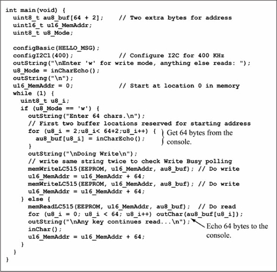
Figure 10.61 shows console output from a test of the Figure 10.60 code. Two 64-byte strings are entered, which means the first four pages of the 24LC515 are written as each string is written twice. The read test reads back the first four pages of the 24LC515. The console output shows the expected string values.
Figure 10.61
Testing 24LC515 read/writes

Ping-Pong Buffering for Interrupt-Driven Streaming Data
The previous examples that performed a write to an I2C serial EEPROM prompted the user to enter a string that was stored in a buffer, wrote that buffer to the serial EEPROM, then prompted the user for another string. However, how would data that is arriving in a continuous stream be handled? Figure 10.62 shows the problem with using only one buffer to handle streaming input data. Once the buffer is full, a page write must be done to EEPROM to save the buffer contents. But new data is continuously arriving and if the current buffer is used to save the incoming data, the old data is overwritten.
Figure 10.62
Using one buffer to capture streaming input data
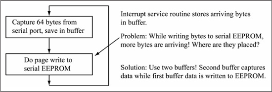
Figure 10.63 shows that the solution to this problem involves using two buffers, named au8_buffer0 and au8_buffer1. Once au8_buffer0 is filled with input data, it is swapped with au8_buffer1 and emptied by writing to it to the EEPROM, with au8_buffer1 used to store input data during the EEPROM write operation. After au8_buffer1 becomes full, it is swapped with the now empty au8_buffer0 and the process is repeated. An ISR captures incoming bytes from the serial port while the foreground code writes the full buffer to EEPROM. This works as long as the buffer used to capture incoming data does not fill before the EEPROM write is finished; recall that in a streaming data application the outgoing bandwidth must exceed the incoming bandwidth or no amount of buffering will prevent eventual data loss due to buffer overflow. The incoming data must arrive by a different communication channel than that used to save the data; in this example, data arrives via the asynchronous serial port and is written to the EEPROM using the I2C port. This buffering strategy is often referred to as ping-pong buffering, because the data bounces between the two buffers.
Figure 10.64 shows the ISR flowchart for capturing streaming data. Two buffers, au8_buffer0 and au8_buffer1, are used to store data, with the u8_activeBuffer flag determining the buffer currently used for input data. A character arrival at the asynchronous serial port triggers an interrupt, which causes the character to be stored in either au8_buffer0 or au8_buffer1, as determined by u8_activeBuffer. The u8_activeBuffer flag always indicates the buffer to which incoming data bytes are written. A buffer becomes full after 64 bytes because that is the page size of the I2C serial EEPROM. The u8_writeFlag semaphore is set once the buffer becomes full; this notifies main() (the foreground code) that the full buffer must be written to EEPROM. The ISR also toggles the u8_activeBuffer flag from 0 to 1 or 1 to 0 so that arriving data is written to the empty buffer while main() empties the full buffer. This is equivalent to swapping the full bucket with the empty bucket in Figure 10.63.
Figure 10.63
Ping-pong buffering to capture streaming data
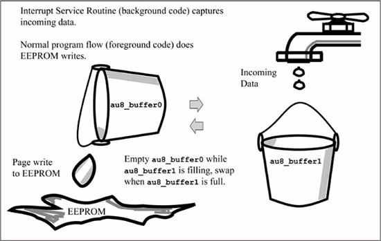
Figure 10.64
ISR flowchart for capturing streaming data

Figure 10.65 shows a flowchart for the streaming write loop in main() that writes the streaming input data to EEPROM. The loop waits until u8_writeFlag is set, indicating that a buffer is full. It then clears the u8_writeFlag, writes the full buffer to EEPROM, and increments the EEPROM address by 64. How do you know if the incoming data rate is not exceeding the outgoing data rate? If the u8_writeFlag is already set after writing the full buffer to EEPROM, buffer overflow has occurred. If overflow occurs, either the incoming data rate must be reduced or the outgoing data rate must be increased. Lowering the baud rate of the asynchronous serial port will reduce the incoming data rate. A new EEPROM with either a faster write time or larger internal page buffer will increase the outgoing data bandwidth. The C code implementation for Figures 10.64 and 10.65 is left as an exercise for the interested reader.
Figure 10.65main() flowchart for capturing streaming data
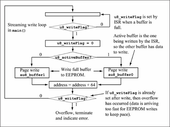
When does the overflow condition of Figure 10.65 occur? Assuming that data bytes are arriving in a continuous stream, overflow does not occur if the following is true:
For a rough estimate, you can ignore processing time and concentrate on transmission time, which gives the following (assuming a 400 kHz I2C bus speed and 1+8+1 serial data format):
The 67 bytes on the right side of Equation 10.6 is the total number of bytes transferred over the I2C bus for a write of 64 bytes as per the write transaction of Figure 10.65 (this ignores end-of-write polling and assumes a worst case write time of 5 ms). Solving for baud rate (BR) gives:
So, the baud rate must be less than approximately 98,000 baud, with 57,600 being the highest standard baud rate from Figure 10.12. In practice, this baud rate provides more than enough margin for this particular application.
Summary
The UARTx, SPIx, and I2Cx modules of the PIC24 μC all implement serial interfaces. The UARTx module uses duplex, asynchronous serial data transfer and is the best choice for PIC24 μC to PIC24 μC communication in terms of application flexibility. The SPIx module implements synchronous serial transfer and offers the highest speed transfer of the three interfaces with a maximum clock speed of 10 MHz. However, it requires a minimum of three wires for the interface, and each new SPI peripheral on the bus requires an additional PIO pin in order to select the peripheral. The I2C module also implements synchronous serial transfer and has the advantage of requiring only two wires for the interface regardless of the number of peripherals on the bus. However, its maximum clock speed is 1 MHz and it has more protocol overhead per byte transferred than SPI transfers. All three serial interfaces are commonly used in microcontroller and microprocessor systems.
Review Problems
Some of the following problems refer to device datasheets found at www.maximintegrated.com, www.microchip.com, www.nxp.com (formerly Philips semiconductor), www.intersil.com, and www.atmel.com. For the I2C questions, use the functions listed in Figure 10.44.
1. What is the bandwidth in MB/s of a parallel data link that consists of 32 wires for data transfer, a clock speed of 8 MHz, and data transfer every second rising clock edge?
2. Assume a PIC24 μC with an FCY of 40 MHz using PORTB<7:0> for data transfer. Suppose you want to transfer 256 bytes of data to an external device. How long does it take to transfer this data, using the code in this problem? Express this transfer rate in MB/s (Hint: you must compute the number of instruction cycles to transfer the data, then convert this to time).
    clr     W0
    mov     #u8_buf, W1       ; Get address of data to transfer
loop:
     mov.b  [W1++], PORTB     ; Write data to PORTB
     dec.b  W0                 ; Decrement counter
     bra    NZ, loop           ; Loop 256 times
   ;;rest of code
3. What is 1 bit time in microseconds for a baud rate of 19,200?
4. How long does it take to send 64 bytes of data at 57,600 baud using asynchronous serial transmission assuming 8 data bits and 1 stop bit if the transmitter pauses for 4 bit times between each character?
5. Give the maximum bandwidth of an asynchronous serial link operating at 115,200 baud in B/s assuming a format of 8 data bits and 1 stop bit with no delay between transmission of the last bit of a previous character .
6. Draw the waveform for an asynchronous transmission assuming 8 data bits and 1 stop bit for the data value 0xA0.
7. Draw the waveform for an asynchronous transmission assuming 8 data bits and 1 stop bit for the data value 0x38.
8. What is the parity bit for the 7-bit value 0x1E assuming odd parity?
9. What is the parity bit for the 7-bit value 0x38 assuming even parity?
10. For an asynchronous serial transfer, assume a 16x clock on the receive side and a data format of 16 data bits + 1 stop bit + 1 start bit. Using a conservative error tolerance of ±5 clocks about the midpoint of the bit time, what is the maximum percent tolerance in frequency mismatch between the sender and receiver?
11. Compute the maximum time before overrun given the UART receiver block diagram of Figure 10.10 and a baud rate of 38,400. Express this time in instruction cycles, assuming an FCY of 40 MHz.
12. For an FCY of 8 MHz and assuming low-speed mode, give the baud rates of Figure 10.12 that cannot be supported either because they exceed 3% error or do not fit in the 16-bit range of UxBRG (use a spreadsheet for these calculations).
13. Repeat problem 12 but assume high-speed mode.
14. Explain how a framing error can occur if the sender’s baud rate is higher than the receiver’s, and repeat for the opposite condition.
15. Look up the specifications for the EIA RS422 standard. What is the principal difference between this standard and the RS-232 standard? What are its advantages, if any?
Answer the following questions about the Maxim MAX5439, a digital potentiometer with a SPI port.
16. Determine the correct settings for the PIC24 μC CKE and CKP configuration bits for interfacing to this device.
17. How many wiper positions does this digital potentiometer support?
18. Is there a method for determining the current wiper register contents? If yes, how is this done?
Answer the following questions about the Maxim MAX5408, a digital potentiometer with a SPI port.
19. Determine the correct settings for the PIC24 μC CKE and CKP configuration bits for interfacing to this device.
20. How many wiper positions does this digital potentiometer support?
21. Is there a method for determining the current wiper register contents? If yes, how is this done?
22. This potentiometer has a zero-crossing detection feature. What does this mode do and why is it included?
23. What is the maximum clock frequency supported for the SPI port?
Answer the following questions about the Atmel AT25256A, a serial EEPROM with a SPI port.
24. What is the organization of this device and total bit capacity?
25. Determine the correct settings for the PIC24 μC CKE and CKP configuration bits for interfacing to this device.
26. What is the maximum clock frequency supported for the SPI port?
27. What is the page buffer size?
28. How is a write-in-progress determined?
Answer the following questions about the Maxim DS3902, a digital potentiometer with an I2C port. Assume that any configurable address selection pins are tied high.
29. How many wiper positions does this digital potentiometer support?
30. Write a sequence of I2C function calls from Figure 10.44(a) that will set the wiper for resistor 0 to a position specified by u8_potVal. Repeat using the transaction functions of Figure 10.44(b). Assume that the ADD_SEL pin of the device is low.
31. Write a sequence of I2C function calls from Figure 10.44(a) that will read the current wiper position for resistor 1 and return it in the variable u8_potVal. Repeat using the transaction functions of Figure 10.44(b). Assume that the ADD_SEL pin of the device is low.
32. What is the maximum clock frequency supported for the I2C port?
Answer the following questions about the Philips PCF8598C-2, a serial EEPROM with an I2C port (find this datasheet at www.nxp.com).
33. What is the organization of this device and total bit capacity?
33. What is the maximum clock frequency supported for the I2C port?
35. What is the page buffer size?
36. How is a write-in-progress determined?
37. How long does a typical page write take?
Answer the following questions.
38. Assuming FCY of 40 MHz, what I2CxBRG value is required for an I2C bus rate of 400 kHz?
39. Devise a scheme for measuring how long a typical self-timed write on the 24LC515 serial EEPROM actually takes. Determine if the typical write time is dependent upon the number of bytes that is actually written.
40. Write code that sets the DS1631 TH and TL registers to values of TH = 100°C and TL = 90°C. You must poll the NVB bit in the status register to ensure that the non-volatile memory is not busy before issuing a write to either of these two registers. Use the I2C functions of Figure 10.44.
41. Assume the DS1631 has been configured for one-shot mode. Write code that starts a conversion then polls the DONE flag until the conversion is finished. Use the I2C functions of Figure 10.44.