
TV SIGNAL PROCESSING
In TV receivers and monitors the final recipient of the video signal is the picture tube, be it a monochrome or colour type. The tube requires a modulating voltage between its grid and cathode; normally the grid is clamped at some fixed potential and the modulating signal applied to the cathode. In a monochrome system that signal will be the video waveform in inverted form – to produce white the cathode must be driven down towards grid potential. In a colour-tube the grid is common to all three beams (Chapter 5) and the cathodes are fed by RGB video signals, negative-going for white.
TUBE-DRIVE AMPLIFIERS
Large picture tubes require a peak to peak voltage drive approaching 100 V to produce a bright contrasted picture, small monochrome tubes 50–70 V. It is the job of the final video amplifier to provide this drive, and for full detail in the picture its frequency response should extend from d.c. to beyond 5 MHz. For data-monitors, and for sharp display of teletext and computer-generated characters and graphics, the video amplifier response must be better – to 10 MHz and more.
The stray capacitance of the video amplifier’s load, represented by the tube cathode, base connections, transistor heat sink and associated wiring can exceed 10 pF, whose reactance at 5.5 MHz is 3 kΩ, and at 12 MHz is less than 1.5 kΩ. To avoid curtailment of h.f. response, then, the final video amplifier must have a very low output impedance to ‘swamp’ the capacitance of the load. Class A amplifiers have relatively high output impedance with practical values of collector load resistance and operating current, though they are used in domestic monochrome TVs and basic colour sets, where h.f. response is enhanced by the use of peaking coils in the collector circuit; and/or frequency-selective negative feedback by virtue of a suitable bypass capacitor across the emitter resistor. For more exacting requirements class AB video amplifiers are usually specified.
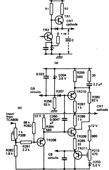
Fig. 7.1(a) shows the form of a commonly used variant with two npn transistors. TR2 functions as a class A amplifier with R1 as collector load. When the transistor is being driven on (i.e. picture brightening) its low impedance to ground rapidly discharges stray capacitance C. For a picture transition towards black, however, TR2 c-e impedance rises, and stray C can only slowly charge via load R1, resulting in a blurred trailing edge on the picture feature. TR1 remedies the situation by conducting at this time via low-value resistor R2 to provide a shunt across R1 and a quick charge path for C. Fig. 7.1(b) gives a full circuit of one of the three primary-colour output stages in a commercial colour TV. TR208 forms an emitter-follower driver stage whose output is developed across R284. TR209 is the basic video amplifier with collector load consisting of the parallel combination R280 and TR210. The current flowing through this circuit remains fairly constant. HF signals are applied to TR210 base via C260. D204 and R258 provide bias for pnp TR210, and D207 offers a degree of d.c. restoration. R289 and R285 equalise the current swings in the two transistors. R286 and R287 limit peak current, and hence power dissipation – and provide some protection in the event of short-circuits. The stage is stabilised by d.c. feedback via R283 to TR208 base, and the values of R281, 282 and 283 are chosen so that no current flows through P209 at black level.
The potentiometers P209 and 210 represent the difference between a video output stage in a good quality monochrome receiver or monitor, and one of the three matched RGB amplifiers driving the tube of a colour set. In the latter case it is necessary to equalise the light output of the three colour phosphors near black level by background controls – P210 and its equivalents in the other stages – which set the tube cathode voltages at black level; and also to provide separate contrast (drive) controls for each primary colour. These grey-scale tracking controls are adjusted for true white (illuminant D) from the colour-tube display at all levels of video drive. The background controls are trimmed for neutral colours in the lowlights and then the drive controls (P209 in Fig. 7.1 and its equivalents) for true white in the highlight picture areas. Only when the grey-scale is correct will true colour reproduction be achieved. In sets incorporating auto-grey-scale tracking (see later, this chapter) the need for the background controls is removed.
CLAMPING AND BLANKING
In a monochrome monitor or TV the route from video input socket or detector to picture-tube includes a low-level video amplifier as an interface between the source and the output stage. Here or at the output stage itself, two services are required. Because the response of the entire video path is unlikely to extend to d.c. and very low frequencies, the video signal must be clamped. At some known reference level in the waveform (i.e. back-porch or line sync pulse tip) the signal is returned to a fixed voltage by a diode or transistor switch. DC restorers operate on a passive basis; driven clamps have better performance, using an electronic switch driven by a suitably timed pulse from the line scan or sync separator stage of the set. Clamping ensures that picture black-level always coincides with the cut-off point of the picture-tube, and remains stable with respect to time, temperature and picture content.
Blanking takes place at line and field scanning rate, and cuts off the video amplifier except when picture information is actually present. Thus spurious images from the flyback action of the scanning spot (during which burst, teletext and other signals are present) are suppressed.
What has been described so far in this chapter, and in Chapter 3, completes the signal processing arrangements for monochrome TV sets and monitors.
COLOUR DECODING
Most of the post-detector signal processing stages of a colour TV or monitor are concerned with recovering RGB video signals from the encoded CVBS signal coming from the receiver section, videorecorder or camera. The description which follows is based on the PAL system.
The CVBS signal is resolved into U and V colour difference signals by the first part of the decoder, illustrated in the block diagram of Fig. 7.2. The processes carried out here may be briefly summarised as follows:

1. Chroma amplifier with bandpass filtering based on 4.43 MHz to separate the chroma signal from the composite waveform and to provide initial amplification.
2. The output from the chrominance amplifier is fed to a delay line and signal separating network which separates the U and V signals by a process of adding and subtracting the direct (real-time) signals to and from those which have passed through the delay line. Here also is carried out the hue-averaging process between successive lines of chroma information.
3. The R–Y and B–Y outputs from the signal separation circuit are applied to synchronous demodulators which sample each at regular and short intervals according to the timing of their drive (reference) signals, derived from the reference oscillator. As there is a 90° phase difference between transmitted U and V signals the reference feeds to the synchronous demodulators are likewise in quadrature. In this way the upper demodulator is made conductive only for U signals, and the lower only for V signals.
4. As the burst signal is required to synchronise the reference oscillator, a burst gate is needed to separate the colour burst from the rest of the chroma signal; this can be achieved by gating the stage with a pulse from the line timebase section so that it is switched on only during the back porch period when the burst signal is present.
5. As the subcarrier is suppressed at source it is necessary to provide a local oscillator as a source of reference carrier for the synchronous demodulators. This reference oscillator must operate at the same frequency and with the same phase relationship to the chroma signals as the subcarrier itself. For accuracy and stability a crystal oscillator is used; its phase – and its frequency within narrow limits – can be ‘steered’ by means of a phase detector and reactance control circuit.
6. The burst signal switches phase between ±45° on alternate lines, giving rise to a signal at 7.8 kHz (half line frequency) appearing as a ‘ripple’ at the output of the phase detector. This, the ident signal, is taken off by the 7.8 kHz acceptor filter and used to control the colour-killer and PAL switch phase-inverter circuits.
7. The colour killer circuit, controlled by the ident signal, operates to cut off the chroma signals during reception of monochrome pictures. This is necessary to prevent spurious signals (i.e. h.f. components of the luminance signal) and noise in the chroma circuits – whose gain in these circumstances will be at maximum under a.g.c. (a.c.c.) control – from generating cross-colour and confetti effects on the picture. When the ident signal disappears the colour killer shuts down the chroma amplifier.
8. Since the PAL system depends on phase reversal of the V chroma signal on alternate lines, it is necessary to incorporate a phase inverter (180° phase shift) controlled by a bistable switch which brings it into operation on alternate lines. The bistable switch is triggered by a pulse from the line oscillator, and is locked into the correct phase by the 7.8 kHz ident signal. The PAL switch may alternatively be incorporated in the V signal feed line, where it will have the same effect of restoring correct polarity to the V (hence R–Y, and finally R) chroma signal.
Many variations in decoder design are possible, as will be seen when IC decoders are investigated shortly.
Delay line and U/V separation
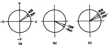
The line-by-line phase inversion of the V chroma signal in PAL-encoded transmissions was described in Chapter 6. The errors introduced by differential phase distortion in the signal path remain relatively constant so that they will have opposite effects according to which of the two V axes is in use for transmission. For instance if a blue area is being transmitted it may be shifted towards cyan during one line, but towards magenta on the succeeding line. If such a signal is displayed on a picture-tube the human eye will tend to integrate and average out the opposing hues and see the correct blue hue. Large phase errors would give rise to a noticeable venetian blind effect, sometimes referred to as Hanover bars. The equal-and-opposite errors can be effectively cancelled out electronically by means of a one-line signal delay and associated matrixing circuits. Consider Fig. 7.3. Fig. 7.3(a) has a phasor A (solid line) transmitted on line n at 30°; phase distortion in the signal path causes it to be received as dotted phasor B at 40°. The same hue transmitted on line n + 1, now A’ at −30° with respect to the U axis, appears in Fig. 7.3(b) along with the phase-distorted resultant as a dotted line phasor B’ at −20°. After reversing diagam b’s vector about its U axis, the two received signals B and B’ correspond to B and B” (Fig. 7.3(c)), which when averaged give the correct hue A at 30°.
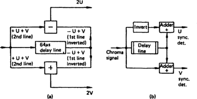
The essence of the decoder in a PAL receiver, then, is in the separation of the chroma signals modulated on the subcarrier, and in so processing them that the electrical average between each successive pair of lines is applied to the synchronous demodulators. It depends on the use of a delay line with which a one-line-old chroma signal can be made simultaneously available with a real-time signal. The delay line is made of glass; an input transducer converts the electrical subcarrier signal to an acoustic (mechanical) one, whence it is propagated relatively slowly through the body of the glass block in a zig-zag path, being reflected, snooker-ball style, whenever it encounters the glass wall. The path length is such that the transition time is exactly 63.943 µs ±3 ns. At path-end the mechanical wave is reconverted to an electric one by a piezo microphone. The 63.943 µs delay time corresponds to 283½ cycles of reference subcarrier: the odd half-cycle is very important, ensuring that the emerging signal is in opposite phase to that of the undelayed (real-time) subcarrier signal. Since the U signal is always transmitted in the same phase, addition of these direct and delayed signals (Fig. 7.4(a)) will cancel out U components altogether. V signals will be present, however, because the phase reversal introduced during encoding will effectively cancel out the phase reversal due to the half-cycle offset at the delay line’s output. The time-coincident V subcarrier cycles, then, will sit on each other’s shoulders in the adder to render a pure 2 V output. Now consider the subtractor in Fig. 7.4(a). It receives the same two signals as the adder, but here the subtraction of each V subcarrier cycle from its identical and time-coincident fellow will render zero V output. Antiphase U cycles, however, when subtracted will reinforce each other to render 2U as sole output. An earlier chapter revealed a subtractor to be a combination of inverter and adder, and they are thus drawn in Fig. 7.4(b), making clearer the separation of the U signal. Since the chroma signals of two consecutive lines contribute to all U and V outputs the required averaging outlined in Fig. 7.3 is achieved simultaneously with the separation process.
Synchronous demodulation
Every NTSC or PAL decoder contains synchronous demodulators which are basically on-off switches, closed briefly once per subcarrier cycle by the reference waveform. The timing of the ‘on’ period is governed by the phasing of the local reference feed, which is locked in the required phase by the burst signal via a phase-locked-loop (PLL). Because the U and V subcarrier signals are in quadrature the peak of one coincides in time with the passage of the other through the zero line. Referring to Fig. 7.5, it can be seen that closing the U switch at times t1 and t2 will sample the U signal without crosstalk from the V signal, and that closing the V switch at time t1 and t3 will likewise sample only V level. The U and V signals, of course, represent colour-difference signals which can have either positive or negative values – on a yellow subject, for instance, R–Y and G–Y will take the form of positive voltages to turn on the red and green guns of the picture-tube, while B–Y will take up a negative voltage to turn off the tube’s blue gun. Study of Fig. 7.5 shows that the synchronous demodulator is capable of producing positive and negative outputs, and in practice each demodulator’s output varies rapidly in terms of amplitude and polarity as the chroma subcarrier signal (there is only one in spite of the diagrams of Figs 7.4 and 7.5) changes its phase and amplitude to describe the hue and saturation of the picture elements in turn.
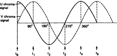
Fig. 7.5 Principle of synchronous demodulation of signals in quadrature. Each carrier is modulated separately, and two demodulators – one synchronised with each carrier – sample the waves only at the times when one is at maximum and the other at null, thus separately recovering the two information streams. The solid-line (U) signal is sampled at times t0, t2, t4, and the broken-line waveform (V) at times t1, t3, t5
Crystal oscillator
A resonant crystal consists basically of a tiny slice of quartz mounted between metallic plates, and enclosed in a sealed envelope. Like a tuning fork the quartz slice has a mechanical resonant frequency; unlike the fork, it is barely affected by temperature variations, and behaves like an extremely high-Q tuned electrical circuit. While its stability is very good, it cannot by itself provide a reference signal of correct frequency and phase. Fortunately the resonant frequency of a suitable crystal can be slightly ‘pulled’ by capacitive loading; the use of a varicap diode for this purpose permits voltage control of oscillator frequency. This combination forms a voltage-controlled crystal oscillator (VXO) and is used in combination with a phase detector to make a much-used building block in electronic circuits – the phase-locked-loop. Its principle was described in Chapter 3, and here the PLL is used to lock the local crystal to the mean phase of the transmitted burst signal. To prevent the local reference crystal trying to follow the swinging phase alternations of the PAL burst signal a suitably long time constant is present in the error voltage path.
G–Y and RGB matrixing
Before a G–Y signal can be made from the red and blue colour-difference signals the transmitted U and V chroma components must be de-weighted. It was explained in the last chapter that a reduction in amplitudes of R–Y and B–Y signals is made to prevent them from overdriving the transmission system. After passing through an amplifier with a gain of 1.14 the V signal is ‘normalised’ to R–Y Similarly, B–Y appears at the output of a ×2.03 amplifier fed from the U signal.
Recovery of the G-Y signal depends on the basic equation given earlier: Y = 0.59G + 0.3R + 0.11B. In fact, G–Y can be directly derived from R–Y and B–Y. Adding 0.508 of (–R–Y) to 0.186 of (–B–Y) renders G–Y. Correct proportions of inverted R–Y and B–Y signals meet in an adder and combine to render the G–Y signal. Finally, the three colour-difference waveforms are each added to the luminance signal to make the primary-colour signals R, G and B for application (in inverted form) to the picture-tube cathodes.
Because the bandwidth of the luminance channel is kept wide to ensure that a detailed black-and-white picture is displayed as a base on which the coarser colour information is superimposed, the transit time of the Y signal is much shorter than that of the chrominance signals, constrained in a channel about 500 kHz wide. When the Y and colour-difference signals come together in the RGB matrix this would result in them being out of step to cause misregistration on the screen. To prevent this a short delay line (t about 500 ns) is provided in the low-level luminance path. The glass delay line described previously is not suitable for a wideband signal; the type used here has series inductance and parallel capacitance distributed along it, and takes the form of a low-inductance coil wound over a grounded foil. Alternatively, a bucket-brigade device (of the type described in connection with CCD image sensors in the previous chapter) is used, with its advantages of small size and IC construction.
Subcarrier trap
On highly saturated colours a large amplitude subcarrier signal is present and appears on the screen as a fine dot-pattern. Although the pattern itself is barely distinguishable at normal viewing distances the non-linearity (gamma) of the tube will have the effect of partially ‘rectifying’ this subcarrier signal, artificially brightening up highly coloured parts of the picture. A notch filter, sharply tuned to 4.43 MHz, forms a trap in the luminance signal path; in some decoder designs provision is made to switch off this trap during reception of monochrome transmissions, thus realising the full definition capability of the shadowmask tube. The trap-switching is carried out by the colour-killer line.
BRIGHTNESS, CONTRAST AND COLOUR CONTROL
Provided that the black areas of the picture can be made to drive the picture-tube just to beam cut-off (and this can be achieved automatically, see later), and if viewing were always in low or zero ambient light, the only picture control necessary would be a contrast control, with a link to the colour (saturation) control line. Because viewing conditions vary greatly, as do viewers’ tastes, all three controls are generally provided, though often relegated to semi-accessible presets. For brightness control, the d.c. level on which the entire picture sits is raised and lowered, generally by altering the pedestal clamp reference voltage. For control of contrast the gain of the Y-signal amplifier must be varied while maintaining correct black-level; because any adjustment of contrast requires a proportional adjustment of colour level, the user contrast control will generally influence the chroma gain by means of an electrical ‘tracking link’ between the two. Colour level (user control) and colour/contrast tracking are carried out by varying the gain of the chrominance amplifier.
There are several internal influences on these analogue control lines. Excessive beam current in the picture-tube is detected by a sensing circuit which pulls down brightness, contrast or both to prevent excessive dissipation in the picture-tube’s shadowmask. Some sets have ambient light sensors to adjust contrast to suit the viewing conditions. As an internal loop in the decoder, an a.c.c. (automatic colour control) circuit monitors the amplitude of the burst signal and adjusts chroma gain accordingly; this maintains correct saturation level in the face of chroma signal amplitude variations due to propagation conditions, mistuning etc.
COLOUR DECODER
The low-level signal processing stages in a colour decoder are ideally suited to IC technology. An internal diagram of a typical chip is illustrated in Fig. 7.6.
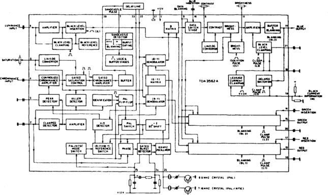
The luminance signal is applied at pin 8, having passed through the delay line and subcarrier trap. The input coupling capacitor also serves as reservoir for the black-level clamping carried out within the chip. Luminance black-level is referred to an internally generated voltage pulse. Thus conditioned, the Y signal passes on to the R, G and B primary-colour matrices.
The chroma-separating bandpass filter feeds 4.43 MHz chroma signal and burst to IC pin 4. The first function within the chip is a.c.c, whereby chroma signal amplitude is regulated according to received burst level as seen by the peak detector – the control potential reservoir is the capacitor at IC pin 3. Regulated chroma signal now enters a voltage-controlled attenuator to come under the influence of the d.c. voltage coming in to pin 5 from the user control – this may be cabinet-mounted or part of a cordless remote control. The effect of the saturation control is removed once per TV line – for the duration of the burst signal. Thus the amplitude of the burst is unaffected by the setting of the colour control, and it travels, along with whatever level of chroma signal has been set, through the chrominance amplifier and buffer stages and out of the chip on pin 28 for application to the external glass delay line and matrix circuit. Separated and averaged U and V signals re-enter the chip on pins 22 and 23 respectively, for passage to the de-weighting circuits and synchronous demodulators. Once demodulated, the B–Y and R–Y signals take two paths – to the G–Y matrix and to the primary-colour matrices, where each colour-difference signal is recombined with the luminance signal to make R, G and B signals for onward progress towards the picture-tube.
Because the burst signal has a ±90° phase shift, it does not get ‘averaged’ in the delay line matrix. It is input to the phase-locked-loop for subcarrier regeneration and services the entire ‘reference’ circuitry in the lower left-hand section of the chip diagram. It first encounters the burst gate where signal chroma is eliminated.
The subcarrier oscillator in this circuit runs at twice subcarrier frequency, 8.867238 MHz. Its frequency is divided by two and 90° phase shifted on its way to a phase detector wherein it is compared with incoming burst: the RC network between pins 24 and 25 form a low-pass filter whose long time-constant keeps the PLL steady at mean burst phase. Thus is the loop completed, with the advantage that the 2 × fsc locked oscillator can render, via ÷2 circuits, correctly phased quadrature reference feeds to the two demodulators. En route to the V (R–Y) demodulator the reference feed is inverted on a line-by-line basis by the PAL switch, driven in turn by a bistable flip-flop circuit.
The flip-flop acts as a ÷2 stage on line-rate trigger pulses, but must be steered by an ident detector to ensure that the PAL switch phase is correct. Ident monitoring is carried out in the H/2 detector, which compares V signal polarity with V demodulator drive phase. When the two disagree a reset pulse is passed to the ident stage, thence to the flip-flop. The latter misses one beat, thus ‘phasing up’ to the incoming PAL signal. Once PAL ident has been corrected, the colour-killer block opens the synchronous demodulators permitting colour to reach the screen.
A second function of the H/2 detector is that of a.c.c. control element. Its output is proportional to burst amplitude and is turned into a control voltage by a peak detector for application to the controlled chroma amplifier. This loop maintains constant burst amplitude, hence correct saturation level in the picture.
The crystals and transistors at the bottom of the diagram indicate the dual-standard capabilities of this IC. A switching voltage introduced at pin 25 will put the chip into NTSC mode, with PAL switch disabled, time-constant removed from the PLL error voltage line, and 3.58 MHz or 4.43 MHz reference selected by turning on the appropriate crystal-switching transistor. The necessary tint control is switched in across pins 24 and 25.
From the Y matrices the RGB signals (only B shown in full detail in Fig. 7.6) each enter a data switch. At a command from pin 9 this changes stage, passing to the output stages locally generated RGB signals applied to pins 12, 14 and 16; they may typically come from an inbuilt teletext decoder or from a personal computer via a rear-mounted multipin plug/socket. These signals come under the influence of the contrast and brightness control stages next downstream in each channel. According to the d.c. voltage presented on pins 6 and 11 of the chip, these adjust the gain and d.c. operating points of all three RGB channels in parallel. These stages are necessarily perfectly matched by virtue of their simultaneous fabrication on a single silicion substrate. The controlled signals now pass through a clamping amplifier, blanker and buffer stage before passing out of the chip on pins 13(R), 15(G) and 17(B) to the high-level tube drive amplifier stage described at the beginning of this chapter.
The penultimate clamping amplifier has the special function of automatically setting up the black-levels for each colour according to the gun cut-off characteristic of the picture tube in use. During the field blanking interval each gun of the tube in turn is driven just to cut-off point by a specially shaped and timed pulse from the IC. The measured cathode current is fed back into the IC on its pin 18 (black current information input); three pulses are received in quick succession, one for each gun, and are directed to the appropriate clamps in the IC. The measured currents are in each case converted to a clamp reference voltage, stored for R, G and B on the capacitors at pins 10, 20 and 19 respectively. By this means the three colours on the screen are made to cut off at exactly the same point on the reproduced grey-scale, regardless of ageing or manufacturing tolerances in the tube, and with no need for manual adjustment. The less commonly required (and less noticeable on viewing) need for drive adjustment to neutralise highlight tinting must still be provided – and made when gun emission or phosphor efficiency drops.
All control pulses for blanking, keying, clamping and gating enter the IC on pin 7. The waveform here is a ‘sandcastle’ shape, whose lower level contains line and field-rate blanking pulses, and whose upper level contains a short line-rate pulse coinciding with the period of the colour burst. It is sorted out by level detectors within the IC, and generated by the horizontal sync processing chip in the set’s time-base section.
MULTIFUNCTION PROCESSING CHIPS
As receiver technology has advanced the decoder IC arrangement illustrated in Fig. 7.6 (itself developed from 4-, 3- and 2-chip systems of earlier years) has been superseded by more highly integrated chips which incorporate the entire colour decoder, along with all the other low-power analogue processing sections of the receiver – Fig. 7.7 gives an example, where it can be seen that the i.f. output from the tuner and SAW filter enters at the left and RGB video waveforms emerge at the right. Along the way are carried out sync separation and time-base generation, f.m. sound demodulation and processing, and multi-standard chroma decoding.
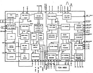
Fig. 7.7 Signal-processing IC incorporating all the low-level vision stages and the timebase generators
The section which interests us here is in the bottom right-hand side of the diagram, where lies the dual-standard PAL/NTSC decoder with auto-recognition of the system in use; the 4.4 MHz crystal at pin 35 is for use with PAL, and the 3.6 MHz one at pin 34 for NTSC. The LC components connected to pin 36 form the loop filter for the burst phase detector, and correspond to the network at pins 24/25 of the IC in Fig. 7.6. All the user control functions (i.e. saturation) enter this IC via the I2C port at chip pins 7 and 8 in the form of serial data from the microcontroller IC – more details in Chapter 22.
The TDA4665 device connected between pins 29/30 and 31/32 in Fig. 7.7 is a 64 us delay line using a ‘bucket-brigade’ (CCD) technique. Inside it are two sets of 192 capacitors in a progressive ladder arrangement, each capacitive rung connected to the next by an electronic switch. The switches are closed in sequence over a 64 µs period by an in-built clock oscillator at 3 MHz rate, line-locked by a sandcastle pulse. B–Y and R–Y signals are fed onto the ladder and ‘chopped’ into samples by the action of the first switch, then stepped sequentially along their own capacitor-ladders, re-entering the main IC after a one-line delay. Thus the function of the glass delay line described earlier is achieved by cheap electronics rather than costly mechanical/acoustic means. Wideband ‘short’ delays for luminance signals can also be realised using this technique and incorporated in multifunction processing ICs if required.
After the primary-colour matrix the RGB signals in the main chip pass to switches, controlled by the I2C bus, to permit the injection of RGB signals from (e.g.) a text decoder or a digital TV receiver box. Thereafter the RGB feeds, whatever their source, are controlled for brightness and contrast by the user (via the control bus) and the beam-limiter circuit; and individually for black-level point by a chip-internal process similar to that already described for automatic grey-scale tracking in the chip shown in Fig. 7.6.
SECAM COLOUR SYSTEM
An alternative method of colour encoding, used in France, USSR and elsewhere, involves a similar subcarrier system to NTSC and PAL, but here the colour-difference signals frequency-modulate the subcarrier whose centre frequency is 4.437 MHz. The R–Y and B–Y signals are sent sequentially, i.e. R–Y on line n and B–Y on line n + 1 etc. To identify which chroma line is which, special ident signals are transmitted during the field blanking period (original system: France, USSR, Luxembourg) or the line blanking period (Albania and the Middle East).
To decode SECAM signals the chrominance subcarrier is filtered out in a tuned trap centred on 4.437 MHz, then applied to a re-shaping (‘bell’) filter (see Fig. 7.8) to compensate for the characteristic of an opposite-law filter introduced at the transmitter – their object is to improve chrominance S/N ratio. A pre-emphasis system is also used to the same end. The SECAM chroma signal now takes two paths – one direct and one via a one-line (64 μs) delay system. For any given TV line, then, both R–Y and B–Y signals will be available: one at the delay line output and one via the direct path. The double-pole, double-throw switch S1 is toggled at half-line rate (7.8 kHz) and steered by the SECAM-ident signal.
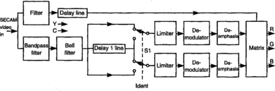
Fig. 7.8 Principle of SECAM decoder – the ident signal is derived from the broadcast signal once per field (SECAM V) or once per line (SECAM H)
The now continuous R–Y and B–Y f.m. signals next pass through separate limiters on their way to f.m. demodulators, whose baseband output signals are then de-emphasised in the final noise reduction process. As with NTSC and PAL colour-difference signals, they are now de-weighted and matrixed with the (delayed) Y signal to make up R, G and B signals for driving the display tube.
The advent of multistandard TV sets and videorecorders for direct reception of terrestrial SECAM transmitters, and particularly for use with satellite broadcasts, brought with it the need for SECAM signal handling even in countries whose own broadcast system is otherwise. Although videorecorders do not decode the chroma signal, their colour-under circuits vary with the encoding system in use, and in the particular case of Video 8 format machines, SECAM signals have to be transcoded to PAL before commitment to the tape, and recoded to SECAM during playback.
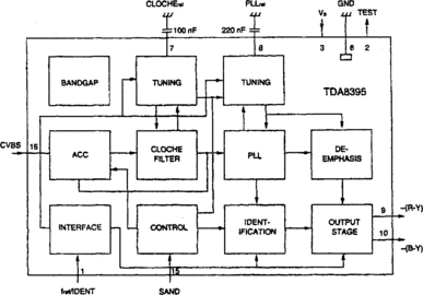
Where multistandard colour decoding is required there are several possible solutions. Fig. 7.9 shows one, designed for use with an IC like that shown in Fig. 7.7, This TDA8395 is a ‘supplementary’ chip, providing SECAM decoding with a minimum of extra components: it uses the existing electronic delay line and reference oscillator, also the sandcastle gating pulse. Composite video enters at its pin 16, together with a stable reference frequency to its pin 1. Negative colour-difference signals emerge from its pins 9 and 10 to pass through the delay line (TDA 4665 in Fig. 7.7) for matrixing and control in the main IC.
SANDCASTLE PULSE
The decoder ICs shown in Figs 7.7 and 7.9 both use a sandcastle pulse for timing and gating purposes. It is generated in the line output stage or the line oscillator section, and takes the form shown in Fig. 7.10. The lower section of the pulse, used mainly for picture blanking during line flyback, is 12 μs wide and embraces the entire line blanking period. The narrow superimposed pulse on its top is used for gating during the period of the colour burst, and is about 3 μs wide; these line-rate pulses are separated by slicers within the chip. In some TV designs the sandcastle pulse has a component at field rate too, used for picture blanking and for extinguishing the scanning beams in the event of a loss of vertical deflection: it prevents burning of the screen phosphors.
