
TIMEBASE CIRCUITS
Every picture-tube must have a means of deflecting its scanning spot to all parts of the screen or target. Except in oscilloscope displays the electron beam is deflected by magnetic fields in the neck of the tube. These are generated by deflection coils wound on a ferrite former and securely fitted to the tube neck. One pair of coils is used for vertical spot deflection, and between them make horizontal lines of magnetic flux in the tube neck: these deflect the beam vertically, in a direction determined by the polarity of the flux lines, and to a degree proportional to the intensity (or number of lines) of flux. For horizontal deflection of the electron beam a second pair of coils is used, this time generating vertical lines of force through the tube neck. Again beam deflection is proportional to strength and direction of the magnetic field. The complete assembly of coils and moulded ferrite former is called a scan yoke. Each yoke is manufactured specifically to match, physically and magnetically, the tube type with which it is intended to be used; this is particularly true of colour tubes, as was made clear in Chapter 5.
The intensity of magnetic field developed by an electromagnet is proportional to the current flowing in it. Since beam deflection is exactly proportional to field strength, the basic requirement for linear image scan is a sawtooth current waveform in each pair of deflection coils. Unless the coils behave as a pure resistor, the voltage appearing across them will not be in sawtooth form – in fact, to create a sawtooth (linearly rising) current in a pure inductor, a constant d.c. voltage must be applied to it.
At very small deflection angles such as those used in camcorder viewfinder tubes a linear deflecting current for line and field scans will result in the required constant velocity of the scanning spot over the target. In large flat-faced display tubes, especially 110° deflection types, a linear deflection characteristic will not impart constant scanning speed over the screen, however: the differing beam path lengths between screen centre and screen edges tends to speed up the ‘linear’ progress of the beam towards picture extremities, and correction must be made for this in the shape of the scanning current waveform passed through the deflection coils.
At field frequency (50 Hz) the scanning coils behave almost as a resistance during the forward stroke, so the required voltage drive approximates to a sawtooth, with compensatory shaping to correct for scan coil inductance and where applicable the ‘fiat-face’ effect. Here the scan output stage acts in similar fashion to a conventional amplifier, e.g. an audio output stage. On the other hand, the line scan-coil pair represent almost pure inductance at the much higher (15625 Hz) horizontal scanning rate; to correctly drive these, then, a constant voltage in one direction must be applied for the 52 μs of the active picture period, then a higher constant voltage in the opposite direction for 12 μs to achieve a complete reversal of magnetic field and a complete traverse of the screen by the scanning spot on its flyback stroke.
Timebases, then, consist of three basic sections: a timing source (in practice some form of oscillator, locked to incoming sync pulses); a shaping stage, consisting of ramp generator for field applications or a pulse generator for line timebases; and a power output stage as a means of driving rapidly changing currents through the scan coils.
RAMP GENERATORS
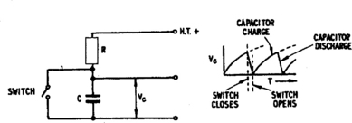
The sawtooth drive waveform required by a field timebase is called a ramp, and of several possible methods of generating it, the simplest is to use a series RG charging circuit. Fig. 10.1 shows the principle, in which capacitor C is allowed to charge towards HT potential via series resistor R. Each time the switch across the capacitor is closed the capacitor rapidly discharges to form the flyback stroke of the scanning spot. As the waveform in Fig. 10.1 shows, however, the sawtooth’s forward stroke is not linear. As the capacitor charges the voltage across the resistor diminishes, with a corresponding reduction of current. In this series circuit the reducing resistor current flows also into the capacitor, and this diminution of charging current with time is responsible for the curvature in the waveform. It can be overcome by charging the capacitor from a constant-current source. In its simplest form this may consist of a very high HT potential and very large resistor R; provided the charging process has not advanced far towards VHT before the flyback switch closes the charging current is substantially constant, and the resulting ramp substantially linear. This configuration is inconvenient for modern IC circuit design, where a constant-current generator is easily arranged in the emitter circuit of an internal transistor.
FIELD OSCILLATOR
Since the ramp-generator function is performed by a capacitor-charging circuit, the only requirements of the field oscillator are that (a) it closes an electronic switch once per 20 ms to discharge the ramp capacitor; and (b) that its free-running frequency be just below 50 Hz to enable it to be synchronised, or triggered, by incoming sync pulses. Many oscillator configurations are possible, though the oscillator must run free in the absence of sync pulses to prevent damage to the picture-tube’s screen when tuning, or during breaks in transmission. All receivers use IC-based field oscillators, in which a form of multivibrator (astable) oscillator is most commonly used. Where a field hold control is provided this adjusts the time-constant of the RC timing network.
An alternative technology is to count line synchronising pulses, triggering the field flyback after 312½ of them. A representative system will be described later in this chapter.
FIELD OUTPUT STAGE
Even though it is most often incorporated inside an IC, the most common configuration for a field output stage in current practice is the class B type, in which a pair of transistors are connected in series across the d.c. supply line with the scan-coil load connected (via a d.c. blocking capacitor) to their mid-point. The circuit design is similar to that of an audio output amplifier, with both transistor bases being driven together by the sawtooth; each output transistor conducts for half the scanning stroke, the crossover point taking place at screen centre. A typical circuit (simplified) is shown in Fig. 10.2, where the incoming sawtooth waveform comes to TR1 base via C1 and R1. TR1 collector load consists of split resistor R4/R5, across which appears an amplified sawtooth for application to the commoned bases of complementary-symmetrical output pair TR2/TR3. At the commencement of scan TR1 collector voltage is high, and TR2 fully conductive as a result. As forward scan progresses TR2 turns gradually off, reducing current in the scan coil via R7, C4 and low-value resistor R11. At the mid-point of scan TR2 is almost off, and TR3 beginning to be driven into conduction – a smooth changeover is ensured by the base-voltage offset introduced by preset R2 and temperature-compensating thermistor R3. For the second half of field scan TR3 is driven progressively harder into conduction by the falling ramp at TR1 collector, to the point where the former is almost saturated at scan-end.
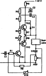
Fig. 10.2 One form of field output amplifier. Here a complementary-symmetrical pair of transistors is used in class B configuration
Flyback is initiated by a sharp drop in drive voltage at TR1 base, rapidly turning it and TR3 off. The upper plate of scan-coil coupler C4 is at almost ground potential, and this large capacitor cannot quickly charge. TR2 saturates and D1 conducts, clamping the top end of the scan coils to HT potential at decoupler C2. The full supply voltage is now present across the scan coils, whose magnetic field rapidly reverses (t flyback = 1 ms) as a result. The bootstrap capacitor C3 ensures that TR2 remains on and TR3 off during flyback; the same capacitor applies positive feedback to the tap on TR1 collector load during forward scan, increasing the circuit efficiency.
The low-value sampling resistor R11 develops a sawtooth voltage proportional to yoke current, passed via R9 as a.c. negative feedback to TR1 base to improve the scanning linearity. A second feedback path, this time with d.c. continuity, comes from the lower end of the scan coils to TR1 base via preset R10. Its purpose is to stabilise the mid-point voltage of the output stage, permitting the output voltage swing to be symmetrical between supply rail and ground. Any rise in mid-point voltage increases conduction in TR1, which pulls down the base voltage of the output pair (and hence their emitters’ voltage) to compensate. Balance is set by adjustment of R10. The second preset R2 sets a small standing (quiescent) current in the output pair to avoid crossover distortion at the point where TR2 hands over to TR3.
The circuit described above is but one variant of many which have been used as field output stages. In most cases the class B output stage is incorporated in an IC which directly drives the yoke via a coupling capacitor; some large-screen receivers and monitors use a class B ‘power booster’ downstream of the IC’s output stage. For camera viewfinder applications a small IC is adequate for the low energy requirement.
IC FIELD TIMEBASE
The field timebase, with its maximum internal power dissipation (in the case of a large-screen colour TV) of about 5 W, is amenable to encapsulation within a single heat-sinked IC like that illustrated in Fig. 10.3. The oscillator is triggered by field sync pulses coming into pin 8 via C321, and runs at a frequency determined by the RC time-constant of R349, field hold control VR350 and C331. The ‘switching’ output from pin 12 is a negative pulse of 100 μs duration; it rapidly discharges the ramp-forming capacitor C337/338, which subsequently charges towards supply rail potential via R357 and height control VR356. The sawtooth wave thus formed is buffered within the chip to emerge at pin 1, where it is applied via R361 and linearity adjustment pot VR362 to the tap on the ramp-charging capacitor as a source of linearising feedback.
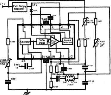
Pin 1 output passes through R368 to re-enter the IC on pin 10 as an input signal to the internal class B power amplifier. Its output, in the form of a ramp-down, appears at pin 4 and is applied directly to the field scan coils whose bottom end is grounded (a.c.-wise) by a large capacitor C341. R367 (1 Ω) samples coil current to produce a sawtooth voltage for reapplication to IC pin 10 as negative feedback. The gain of the output stage is determined by the ratio of input resistor R368 to feedback resistor R364.
The frequency response of this type of IC can extend well into the r.f. range, and to prevent instability and parasitic oscillation the RC combination R354/C336 is included as a frequency-selective negative-feedback path to curtail h.f. response.
Flyback booster
During field flyback a high supply voltage is required for direct application to the scan coils in order to effect a complete reversal of current during the 1 ms flyback time available. A typical pair of field scan coils may have an L/R time-constant around 2 ms, calling for a supply voltage during flyback of roughly double that required for scan-period drive. To avoid the excessive dissipation in the upper half of the power output stage which would result from the provision of a ‘double voltage’ d.c. supply line, the flyback generator technique is used. During the forward scan pin 3 of the chip is at low potential, permitting C334 to charge to supply rail potential (about +20 V) via D305, which also supplies the output stage via pin 5. At the commencement of flyback a switch within the IC links pins 2 and 3, applying +20 V to the negative plate of C334. Since the capacitor cannot instantaneously alter its charge its upper plate now rises to 2 × 20 V = 40 V, reverse-biasing D305 and doubling the available supply voltage at pin 5. When flyback is complete the switch reverts, enabling C334 to replenish its lost charge.
IC field deflector chip
The provision of the vertical oscillator within the field output chip facilitates a simple design for basic and portable TV sets. In other types the oscillator and sync sections are incorporated within a ‘jungle’ chip like that of Fig. 7.7, leaving to the deflection IC only the functions of power drive to the yoke, and flyback generation. An IC of this type is shown in Fig. 10.4; it works to the same principles as the previous example, though the yoke-coupling capacitor is eliminated here because IC pin 5 is at zero volts in the middle of scan. It’s arranged by running the IC from ± 10 V lines derived from a special winding 6/7/8 on the line output transformer and rectifier/smoothing sets D93/C134 (+10 V) and D100/C131 (−10 V). The flyback generator works in conjunction with booster C132/D109 to generate a pulse at IC pin 6 and rapidly pull the scanning beams back to screen top. The pulse is also passed, via C130 and R147, to the teletext and blanking sections of the receiver. R146 and C136 perform the same functions as R354 and C336 in Fig. 10.3.
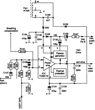
The deflection yoke current passes through R142 to ground, developing a sawtooth voltage at R143 for application to the inverting input of the IC at pin 1 as negative feedback: it stabilises picture height and confers good scanning linearity. Also applied to chip pin 1 is the sawtooth vertical drive waveform coming from the jungle chip via R140/R141/C137. The chip’s non-inverting input pin no. 7 takes an ‘anti-breathing’ voltage via R144 to compensate for the tendency of the picture to shrink at high tube beam currents.
CLASS D FIELD TIMEBASE
Although the class B output stage is efficient, especially when fitted with a flyback booster circuit, some energy is dissipated as heat in the two transistors of the output stage. An alternative and more efficient method of building up an analogue voltage or current waveform is to switch a d.c. supply into an integrator by means of a fast-acting chopper-switch working at high (compared to the alternations of the basic analogue waveform) frequency. The ratio of on-time to off-time in the switch determines how much energy is built up by the integrator. A class D field timebase IC was developed along these lines. The TDA2600 contains a 150 kHz oscillator as chop-timer and an r.f. switch whose duty-cycle is varied according to a 20 ms ramp generated within the chip by conventional means.
A later approach to switch-mode field scan technology is illustrated in basic form in Fig. 10.5, where the vertical deflection coils (yoke) have one end (A) permanently connected to a source of +21 V d.c. By varying the charge on capacitor C1, current can be made to flow through the yoke in either direction. As an example, variation of C1 charge between +30 V and +10 V in linear fashion over a 20 ms period would build up a sawtooth scanning current, symmetrical about Izero, in the coil.
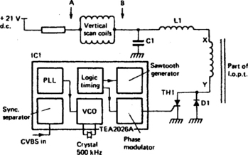
The charge on C1 comes from winding X–Y on the line output transformer, which is so phased that during each line flyback period pin X goes 190 V positive of pin Y. If thyristor TH1 remains permanently off, diode D1 will act as rectifier and C1 will become charged to +190 V via L1. If, however, TH1 stays permanently on, LOPT pin Y is fully grounded: the pulse voltage at pin X positions itself symmetrically about ground potential (d.c. zero line) and the charge on C1 falls to zero. By varying the conduction period of TH1 the charge on C1 can be varied throughout the 20 ms field period. Since TH1 is always turned off at the beginning of line flyback by the negative pulse from LOPT pin Y, its conduction period depends on the timing (phasing) of its positive gate turn-on pulse.
In this circuit, at the start of each field scan the TH1 trigger pulse comes late in each line, so a high voltage develops across C1; current flows from B to A (conventional current flow) through the scan yoke. As field scan continues, TH1 trigger pulse timing (during each line period) is progressively advanced to linearly reduce C1 charge. Halfway through field scan (t = 10 ms) C1 charge equals +21 V and no current flows in the yoke; continuing advancement of TH1 gate pulse phase reduces C1 charge below +21 V, and an increasing current flows through the yoke from A to B. This reaches its maximum at the end of field scan (screen bottom) when TH1 gate pulses are cut off, C1 charge rapidly reverts to +190 V and a large current passes through the yoke in direction BA to give rapid flyback.
As Fig. 10.5 shows, the pulse generation and timing are carried out in IC1, type TEA2026A. The basic field scan timing is governed by a quartz crystal oscillator and phased to incoming field sync. To control the timing of the line-rate thyristor drive pulses a field-rate ramp is generated within the IC; its level is sampled at line rate in the field logic timing section. The sample level is processed in the field phase-modulator to form thyristor triggering pulses. This same IC is also responsible for sync separation; line flywheel synchronisation; line pulse generation; and control of the switch-mode power supply circuit.
LINE TIMEBASE
As for the field section, the function of the line timebase is to deflect the scanning spot of the picture-tube, and it has the same three basic building blocks of synchronised oscillator as timing source, shaping/driver stage and power output amplifier. Line timebase circuit designs are quite different to field ones, however, due to the much higher frequencies involved.
All line timebases which rely on CVBS-borne syncs incorporate flywheel synchronisation. Instead of using individual sync pulses to trigger each line scan, the frequency and phase of the locally generated line drive pulses are compared with those of the incoming sync pulses in a phase detector. Its error signal acts on the local oscillator to pull the two streams of pulses into phase-coincidence. This is another example of a phase-locked-loop, and here the time constant is chosen to be long compared with the period of one line; by this means the effect of interference or noise on incoming sync is minimised, since the triggering of any one scanning line is determined by the mean timing of many preceding line sync pulses.
The arrangement of a representative IC containing sync separator, flywheel sync, line oscillator and noise suppression gate is shown in Fig. 10.6. The sync separator section contains a ‘slicing’ stage to strip away the video signal component of the CVBS waveform applied to pin 8. Pure sync signals emerge on pin 7, whence the field components (long-duration pulses) are separated out by an integrator for application to the field oscillator. The short-duration line sync pulses alone are picked out by a differentiator feeding IC pin 6, where begins the business of line synchronisation. The IC has three control loops, each containing a phase comparator; the first is part of a PLL providing flywheel sync by comparing timings of line oscillator pulses and incoming sync pulses from pin 6. The error-output voltage from this first comparator (pin 12) passes through an external low-pass (flywheel) RC filter to re-enter the chip on pin 15 where it finely controls the oscillator frequency. Free-running oscillator frequency is governed by a close-tolerance capacitor at pin 14 and a potentiometer network (line hold control) at pin 15.
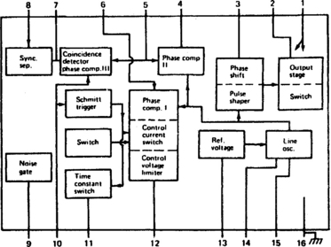
The second comparator examines the timing difference between flyback pulses from the line output transformer (applied at pin 5) and oscillator pulses. Its error output represents unwanted phase shift in the driver and output stage, which may vary with picture brightness etc., and is externally low-pass filtered between IC pins 4 and 3. At IC pin 3 this second control voltage operates on a phase shift/pulse shaper section which corrects the phase of the oscillator output pulses. Phase-locked drive pulses emanate from pin 2 for onward passage to the line driver stage, to be examined shortly. At this point the waveform is square, switching cleanly between two voltage levels and completing one cycle every 64 μs. Sawtooth waveshaping for the line scan coils is carried out further downstream – the function of this waveform is purely a switching one.
Mention must be made of the third comparator within the IC. This simply changes the characteristic time constant of the flywheel loop duration – which gives best noise-immunity in situations of high interference or weak received signal strength – to short duration, to facilitate rapid lock-in from the unsynchronised condition, as when changing r.f. channel. Provision is made for connection of an ‘AV’ switch to pin 10 to hold on the short time-constant mode for use with local signal sources whose CVBS signals contain timing jitter. This arises mainly in mechanically driven replay systems like videocassette machines and disc players; a short time-constant in the line PLL enables the line oscillator to follow instantaneous variations in signal timing, and maintains correct positioning of the simultaneously jittering picture elements along each scanning line. The AV switch is electrically linked to an ‘AV-dedicated’ channel selector for automatic switchover. Many sets have a ‘standard’ flywheel time-constant short enough to permit good tape/disc reproduction without the necessity for switching.
Multifunction IC
The functions of timebase generation, as well as many of the other sections examined in this and previous chapters, are embodied in the diagram of Fig. 7.7, reproduced here as Fig. 10.7 for convenience. The baseband video signal entering the chip on pin 13 or 17 is selected under I2C control by the switch near bottom centre of the diagram and passed up to the sync separator and first PLL, whose flywheel characteristic is given by the RC network at IC pin 43. It governs the frequency of the VCO in conjunction with a REF input; the oscillator output passes next through a second phase-control loop which advances or retards pulse timing (relative to sync) to compensate for picture-dependent delays in the line driver and output stages, working on a feedback pulse entering the chip on dual-purpose pin 41 – it also passes a sandcastle pulse out of the chip. The capacitor at pin 42 sets the time-constant for this second phase-lock-loop. The ‘hor-out’ stage consists of a buffer to provide a low-impedance squarewave feed for the line driver transistor to which its output is routed, while the input at pin 50, coming from the ‘bottom-end’ of the EHT generator, has two functions: to provide breathing compensation for both line and field scans; and to shut down the line scan stage in the event of excessive e.h.t. voltage, sometimes known as X-ray protection. It is invoked when pin 50 rises above 3.9 V.

While in this chip it is instructive to look at the field scan sync and driver arrangements. The H/V divider near top right of the diagram counts line pulses to produce the vertical flyback trigger – one of the latter every 612.5 of the former, checked, timing-wise, by pulses coming from the vertical sync separator. Its output is processed in the vertical geometry correction block, where picture-height and linearity control, also S-correction, are applied according to I2C data entering the IC on pins 7 and 8. These values are preset and held in EEPROM memory: more details in Chapter 22. Pin 51 of the chip couples the sawtooth-charging capacitor whose value is typically 100 nF. Emerging on pins 46 and 47 are positive and negative sawtooth field drive waveforms for passage to a yoke-drive IC like that illustrated in Fig. 10.4.
LINE DRIVER
Interposed between the (in-chip) line oscillator and the output section is a matching circuit. Where the output device consists of an ordinary npn transistor (as opposed to a Darlington type) this driver section takes the form of a transistor pulse amplifier with a step-down transformer as collector load. The functions of the line driver are twofold: it isolates the line generator stage from the switching impedance of the output transistor; and provides power amplification to drive the required considerable base current into the output transistor. Fig. 10.8 shows at left a typical line driver and output stage for a colour TV set or monitor. The line driver squarewave is applied to the base of Q402, which it switches fully on and off. The network C404 and R401 damps the primary winding of transformer T401; its secondary winding drives current in and out of the base of Q401, the line output transistor, here directly but in some designs via a network (which may involve R, C, L and D elements) to shape, damp and control current in the b–e junction of the output device.

LINE OUTPUT STAGE
The line output transistor acts purely as a fast switch, clamping an inductor across a d.c. power source for approximately one-half of the line scan period. Consider Fig. 10.9(a), in which a line output stage is reduced to its most basic form. Initially the transistor switch is off, and no current flows in L. Passage of a tum-on current through the transistor base links point A directly to ground, placing the entire supply voltage across inductor L. As a result, a linearly rising sawtooth current (t1 to t2 in Fig. 10.9(b)) flows in the coil. Some 26 μs later at t2 the line drive ceases and the transistor switches off. The collapsing magnetic field about L causes an immediate reverse in the direction of magnetic flux and coil-current flow, which now reverses to charge capacitor C; this charging current flows via large capacitor Cres, which effectively links point B to ground for a.c. purposes. At a time t3 determined by the LC time-constant, one half-cycle of oscillation has taken place, and the energy in the capacitor is ready to feed rapidly back into L. Since point B in the circuit is effectively grounded by Cres, this would involve point A going below ground potential: it is prevented from doing so by the action of clamp diode D. The result is that the charge on capacitor C effectively becomes a d.c. voltage source, whose energy is linearly discharged to zero between times t3 and t4. At t4 the circuit is at rest, with no energy left in L or C. This corresponds to the situation at t1, and the transistor is at this point switched on once more to repeat the sequence – at 64 intervals. In this way a sawtooth current is built up in L, which represents the line scanning coils themselves. In practice L is a multi-winding transformer (line output transformer, 1.o.p.t.) to which the scan coils are coupled.
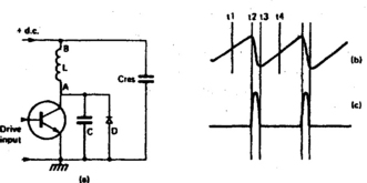
Fig. 10.9 (a) Essentials of a line-scanning output stage; (b) current and (c) voltage waveforms; t1 to t4 represents one 64 µs period
The voltage across an inductor is proportional to the rate of change of current in it. Since this rate of change is constant during the forward scanning stroke, but fast and varying during the retrace (flyback period), the voltage waveform across the l.o.p.t. and scan coils is a series of pulses about 12 μs wide recurring at 64 μs intervals – see Fig. 10.9(c). Plainly the flyback period is determined purely by the LC time-constant rather than any characteristic of the line drive waveform.
Translating line output theory into practical terms, the transistor switch in Fig. 10.8 is Q401, L is formed between pins 2 and 1 of l.o.p.t. T402, D corresponds to D403, and C to C402/404 which together amount to 1.19 nF for tuning. The bottom ends of the latter three may be regarded as grounded – D404 and C405 will be discussed shortly. The line scan coils themselves are in effect connected across the l.o.p.t. primary winding, with their return connector (top RHS of diagram) going via a relatively low impedance path to ground. The components which provide this path will be examined next.
Line scan correction
The circuit of Fig. 10.8 is somewhat complicated by the need to introduce various shaping influences on the line scanning waveform; they will now be explained in turn. L401 is the line linearity corrector, acting as a saturable reactance. Its magnetic field embraces a small permanent magnet which at some point in the sawtooth cycle causes the ferrite core to saturate, whereupon the coil’s characteristic changes from an inductive to a resistive one, with marked effect on the scanning current. In some designs the onset of magnetic saturation is adjusted by rotation of the permanent magnet which thus controls horizontal picture linearity.
The flat face of the picture-tube would show a picture somewhat cramped in the centre and stretched at the sides if a truly linear scanning current were used. To compensate, the rate of change of the line (and field, incidentally) scan current is slowed down at the beginning and end of each sweep, giving a characteristic S-shape to the current waveform. For line scan it is easily achieved by a careful choice of yoke-coupling capacitor – in Fig. 10.8 the 0.27 μF capacitor C408.
Some picture-tubes use deflection yokes which cannot themselves compensate for the geometrical distortion of the image which arises from scanning a virtually flat tube face, especially in wide angle types. To correct the resulting cushion-shaped picture, a diode-modulator is used as a controller of picture width. When fed with a field-rate parabolic waveform it provides dynamic correction of cushion distortion: adjustment of the d.c. working point of this E–W (EastWest) control system sets up the picture width. In Fig. 10.8 the action is based on the elements L402 and C302 in the scan coils’ ground return path.
During the flyback time the magnetic field around the line scanning coils collapses and energy is transferred to C408, the S-correction capacitor. C408 acquires a charge from this energy, and it is this charge, held across the scan coils via D403, which contributes towards the first half of the scanning stroke. Any variation in the charge modifies the current in the scan coils, and hence picture width. During line flyback the energy lost in the scanning circuit is replenished from that stored in the l.o.p.t. This replacement energy is divided between yoke-series capacitors C408 and C302 during flyback. If C302 were shorted to ground the charge across it would be zero and that across C408 at a maximum: the result is maximum picture width. With the short removed from C302 minimum picture width would result. By varying the impedance of a circuit connected across C302 picture width can be varied without altering the tuning or flyback time of the stage, thus keeping e.h.t. voltage (see later) constant. The ‘variable-impedance circuit’ in Fig. 10.8 is in fact the transistor Q403. Its base is fed – via amplifier Q404 – by (a) a field-rate parabolic waveform obtained from the field timebase; (b) a standing d.c. current to set picture width; (c) a small correction current derived from a beam current sensor – it compensates for picture ‘breathing’ effects due to imperfect e.h.t. regulation, and is applied to the height control circuit for the same reason; and (d) in some sets, a sawtooth waveform at field rate, with which any keystone distortion of the picture can be corrected.
In simple designs and older models these horizontal corrections are trimmed by preset potentiometers. More common now, however, is I2C bus control of these parameters, carried out in the ‘jungle’ chip or in a dedicated bus-decoder IC.
Widescreen displays
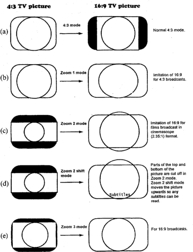
In widescreen (16:9 aspect ratio) display tubes the working principles are the same as described above, though the horizontal scanning current is greater and the amount of correction necessary for S- and pincushion distortion greater. Fig. 10.10 shows the various ways in which older broadcast picture formats can be zoomed under I2C bus control to fill a widescreen display. All of them except Fig. 10.10(e) involve distortion of the picture or loss of part of it. Zoom 1 mode involves changing the linearity of the line scan progressively from the picture centre to its edges, but the displayed image necessarily has geometric distortion. Such are the problems of displaying an image of one shape on a screen of another!
EHT and auxiliary voltage supplies
The l.o.p.t. is a useful source of the many auxiliary voltages and power supplies required elsewhere in the receiver, monitor or viewfinder. Fig. 10.8 shows a secondary winding between l.o.p.t. pins 7 and 9 which provides pulses at 6.3 V r.m.s. to energise the picture-tube heaters. During flyback a pulse voltage (Fig. 10.9c) appears across the l.o.p.t. windings and this can be caught and held by a diode and reservoir capacitor (e.g. D405/C415 in Fig. 10.8) to provide auxiliary supplies. A 205 V supply is thus provided on C415 to operate the RGB amplifiers.
The flyback-rectification system of D405 does not give good regulation of the secondary supply it provides because the flyback pulse is present for less than 20% of the time. For low-current requirements like RGB amplifier feeds and accelerating anodes in tubes this presents no problem because the reservoir capacitor (here C415) can be made large enough to sustain the supply between recharging pulses. For supplies to more energy-hungry circuits like field timebases and audio power-output amplifiers, better regulation is secured by scan-rectification in which the l.o.p.t.-fed rectifier is so polarised as to block the flyback pulse and charge a reservoir capacitor from the much lower (but longer-sustained) voltage present during the scan period. Fig. 10.8 shows two such scan-rectified supplies: D407 and C403 fed from l.o.p.t, pin 4 to provide a 16.5 V supply for the field drive stage; and D408/C413 from l.o.p.t. pin 6 to provide a 46 V line for the field output stage and the line driver section. The phasing of the windings on the l.o.p.t. is indicated by the dots drawn on it in the diagram. In this particular design the audio amplifiers and general processing circuits are powered by secondary windings on the chopper transformer in the main PSU section, to be dealt with in the next chapter.
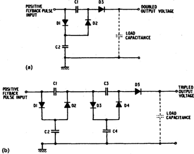
E.h.t. voltages, too, can be obtained by rectifying l.o.p.t. pulses. Flyback pulses are invariably used to obtain the very high final anode voltages needed for modern tubes – ranging from 10 kV for a small monochrome type to 30 kV for the largest colour tubes. Some sets, particularly small portables, have a large secondary winding with many turns (overwind) producing full-e.h.t. voltage pulses for application to a single well-insulated diode, often encapsulated within the sealed l.o.p.t. moulding. A more common technique was the use of a separate diode/capacitor voltage multiplier assembly in the form of an insulated moulded block, use of which requires a smaller (lower-voltage) overwind on the l.o.p.t. Fig. 10.11(a) shows a typical doubler circuit. The load, or smoothing, capacitance is normally provided by the conductive inner and outer coatings on the picture-tube bowl. Its mode of operation is similar to the more common tripler arrangement in Fig. 10.11(b). On the positive flyback input pulse from the transformer overwind, D1 conducts to charge C2 to the peak value of the pulse. During the subsequent scan period the input voltage falls almost to ground potential and the high voltage present on C2 turns on D2 to charge C1 to the peak value of the original pulse. At the next line flyback another pulse appears at the input, ‘jacking up’ the left plate of charged C1: its right plate is thus pushed to twice the peak voltage of the input pulse. D3 charges both C4 and (via D4 and D5) the load capacitance to this voltage. A third flyback input pulse pushes the right plate of C3 up to three times the pulse input voltage for passage via D5 to the load. Thus the ladder-network of diodes and capacitors has tripled the input voltage – typically producing 25 kV from an input pulse train of 8.5 kV peak. In practical tripler circuits, C4 can be returned to D1 cathode instead of ground to reduce the voltage stress upon it.
A second source of e.h.t. is required as a focusing voltage in bi-potential tube types, and in some cases around 8 kV must be made available to give an adequate range of adjustment. It can be derived by a tap from the first diode multiplier stage in the tripler, or by a potential divider chain from the full e.h.t. voltage supply.
Diode-split e.h.t. system
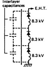
E.h.t. triplers are not very reliable, and most failures in them can be attributed to breakdown of the internal high-voltage capacitors. An alternative and more reliable way of assembling an e.h.t. voltage generator is to build rectifiers into a sectionalised overwind assembly as shown in Fig. 10.12. Here three separate ‘cells’ are present, each consisting of an 8.3 kV secondary winding, an encapsulated rectifier and a capacitor, the latter formed by the windings themselves with insulating layers acting as dielectric. Each cell has only a d.c. potential with respect to its neighbours, and they are connected in series to render the required e.h.t. voltage. The l.o.p.t. in Fig. 10.8 is of the diode-split type, even though the diagram shows a simple ‘shorthand’ version of it. Both focus and screen grid/A1 voltages are derived from built-in adjustable potentiometers, while the ‘bottom end’ of the e.h.t. generator section is hooked to a beam-current monitoring circuit which pulls back contrast and/or brightness to prevent excessive loading on the tube’s cathodes and shadowmask. In a large picture tube the combined beams’ currents may be around 1.5 mA.
An alternative, and now lesser-used, method of deriving tube operating voltages is to rectify pulses at the secondary winding of a chopper transformer, which forms the heart of all modern power converters. They will be examined in detail in the next chapter. In such subminiature circuits as are used in camcorder viewfinders, the auxiliary high-voltage supplies for the display tube are drawn from very tiny multipliers or rectifier/capacitor sets associated with the miniature l.o.p.t.s used; the techniques of line and field timebase and l.o.p.t. secondary functions are the same as described in this chapter, though the very small energy demands of such equipment scales down the currents and voltages involved.
PULSE FEEDS
Many sections of the receiver or monitor require pulse feeds at line rate for gating, clamping and keying. In the luminance stage the signal must be black-level clamped; the line flywheel sync circuit needs a timing reference pulse; the decoder requires gating pulses for extraction of the colour burst and for triggering the PAL switch; some i.f. a.g.c. systems are keyed by line-rate pulses; the scanning spot must be extinguished during flyback; some switch-mode power supply units work synchronously with the line timebase and must be triggered; and so on. Most of these pulses are derived from the line oscillator chip in late designs, but the l.o.p.t. itself may be a source of reference and timing pulses.
In Fig. 10.8 the junction of C416 and C417 provides feedback to the second phase-locked-loop in the line generator section of the jungle IC.
SUPPLY VOLTAGE STABILISATION
The amplitude of the line and field scanning waveform is directly related to the supply voltage to the timebase. While a degree of internal stabilisation is possible within the negative feedback loop of a field timebase, and via the E-W correction circuit of a line time-base, close stabilisation of supply voltage is necessary. This is the function of the power supply circuit, which can be integrated into the line output stage. More commonly, a quite separate PSU (power supply unit) is provided to cope with the greatly varying load presented by a line timebase, whose energy demand depends largely on tube beam current, which in turn depends from moment to moment on picture content. It may vary in a large-screen colour set from 40 W at zero beam current to 65 W when a very bright contrasty picture is being displayed. Where the operating voltage for the field timebase is obtained from the l.o.p.t. it will be indirectly stabilised by the action of the main PSU.
TIMEBASE SERVICING
In field timebases where the fault is complete lack of output (single horizontal line across the screen) the first essential is to reduce screen brightness to prevent damage to the phosphor layer. Once it is established that the operating voltages for all sections of the time-base are present, the next step is to ascertain which section – oscillator, driver or output stage – has failed, for which the oscilloscope is the best tool. Where the entire timebase or amplifier is embodied in a single IC which is proved faulty, check for destructive conditions before fitting and powering a new one. Typical of these are a shorted flyback diode (D305 in Fig. 10.3, D109 in Fig. 10.4), excessive supply voltage, shorted capacitors or heavy output loading due to a leakage or short-path to ground.
More often, field faults will take the form of various kinds of raster-shape distortion. Low supply voltage, faulty electrolytic capacitors or incorrect feedback conditions are the most common causes of these. A top foldover effect with teletext line superimposed is due to slow flyback. A cramping at picture bottom is generally due to an inability of the supply line or the output stage to furnish sufficient current to drive the scan coils fully; this may well be due to a dried-up or ageing electrolytic decoupling capacitor on the supply line to the field output stage.
Where the line oscillator, driver and output stages are not involved in the generation and control of power supplies (see Chapter 11) the diagnosis of a ‘no-go’ fault follows the same pattern of signal (here, pulse) tracing from oscillator via driver to output stage. Line oscillators and drivers are much more reliable than the output stage, which works with relatively heavy currents and high pulse voltages. A quiescent line output section is easy to troubleshoot with test-meter and oscilloscope – such things as dry joints, faulty base drive resistor or open base junction in the output transistor are usually responsible.
More often line output stage faults are manifest as excessive loading, leading to a high current drain on the power supply, which will usually invoke the latter’s overcurrent protection system; the end result, then, will often be a ‘pumping’ symptom, as will be described in the next chapter. First the e.h.t. rectifier or multiplier (if external to the l.o.p.t.) should be disconnected from the overwind. If the set now bursts into life replace the e.h.t. rectifier. Should the stage still not function, the output transistor and efficiency (where relevant, E–W modulator) diodes should now be checked for leakage. The l.o.p.t. can also be loaded by leakage in any other rectifier diodes it may feed, or by heavy loading of their outputs, e.g. a leaky or shorted A1 reservoir capacitor. If after exhaustive testing, and unloading of suspect components, the stage remains heavily loaded, the l.o.p.t. itself is suspect for short-circuit turns or (in diode-split types) faulty internal multiplier components. Shorting turns in the line scanning coils can give rise to similar symptoms, but this is rare; it can be checked by disconnecting the yoke.
During fault-finding it is often prudent to work with reduced voltages and currents in the line output stage to prevent damage, and this can be arranged by fitting a suitably heavy wire-wound resistor in the h.t. feed line to the stage, or by feeding the set from a variac – details in the next chapter.