An FPGA Primer
2.1 Introduction
This section is an introduction to the Field Programmable Gate Array (FPGA) platform for those unfamiliar with the technology. It is useful when designing hardware to understand that the context that the hardware description language models (VHDL or Verilog) is important and relevant to the ultimate design.
2.2 FPGA Evolution
Since the inception of digital logic hardware in the 1970s, there has been a plethora of individual semiconductor digital devices leading to the ubiquitous TTL logic series still in use today (74/54 series logic), now extended to CMOS technology (HC, AC, FC, FCT, HCT, and so on). While these have been used extensively in printed circuit board (PCB) design and still are today, there has been a consistent effort over the last 20 years to introduce greater programmability into basic digital devices.
One of the reasons for this need is the dichotomy resulting from the two differing design approaches used for many digital systems. On the hardware side, the drive is usually toward ultimate performance, that is, faster, smaller, lower power, and cheaper. This often leads to custom integrated circuit design (Application Specific Integrated Circuits or ASICs) where each chip (ASIC) has to be designed, laid out, fabricated, and packaged individually. For large production runs this is very cost effective, but obviously this approach is hugely expensive (masks alone for a current silicon process may cost over $500,000) and time consuming (can take up to a year or even more for large and complex designs).
From a software perspective, however, a more standard approach is to use a standard processor architecture such as Intel Pentium, PowerPC or ARM, and develop software applications that can be downloaded onto such a platform using standard software development tools and cross compilers. This type of approach is obviously quicker to implement an initial working platform; however, usually there is a significant overhead due to the need for operating systems, compiler inefficiency and also a performance reduction due to the indirect relationship between the hardware and the software on the processor. The other issue from a hardware perspective is often the compromise necessary when using a standard platform, for example will it be fast enough? Another key issue when designing hardware is having access to that hardware. In many processor platforms, the detailed hardware is often difficult to access directly or efficiently enough to meet the performance needs of the system, and with the rigid architecture in terms of data bus and address bus widths on standard processors, very often there is no scope for general purpose IO (Inputs and Outputs) which are useful for digital designers.
As a result, programmable devices have been developed as a form of intermediate approach: hardware design on a high-performance platform, optimal resources with no operating system required and reconfigurable as the devices can be reprogrammed.
2.3 Programmable Logic Devices
The first type of device to be programmable was the Programmable Array Logic (PAL) with a typical layout as shown in Figure 2.1. This consists of an array of logic gates that could be connected using an array of connections. These devices could support a small number of flip-flops (usually <10) and were able to implement small state machines. These devices still have a use for specific functions on a small scale, but clearly will be limited for more complex applications. They are, however, still useful for low-cost and compact solutions to a specific digital design requirement.

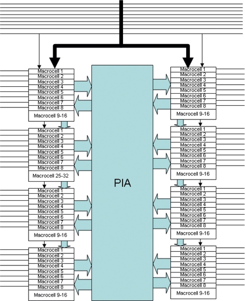
Complex Programmable Logic Devices (CPLD) such as shown in Figure 2.2 were developed to address the limitations of simple PAL devices. These devices used the same basic principle as PALs, but had a series of macro blocks (each roughly equivalent to a PAL) that were connected using routing blocks. With, in some cases, many thousands of logical elements, the CPLD can be extremely useful for implementing a programmable device with custom logic functions and state machines. In some ways, the latest CPLD and early FPGA devices are almost indistinguishable, with one crucial difference. The CPLD is a fixed array of logic, but the FPGA uses complex logic blocks (discussed in the next section of this chapter). However, CPLDs are still of a relatively small scale, and the modern reconfigurable device of choice for high performance is the FPGA.
2.4 Field Programmable Gate Arrays
Field Programmable Gate Arrays (FPGAs) were the next step from CPLDs. Instead of a fixed array of gates, the FPGA uses the concept of a Complex Logic Block (CLB). This is configurable and allows not only routing on the device, but also each logic block can be configured optimally. A typical CLB is shown in Figure 2.3. This extreme flexibility is very efficient as the device does not rely on the fixed logical resources (as in the case of a CPLD), but rather is able to define whichever logical functions are required as part of the logic block reconfiguration.
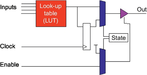
The CLB has a look-up table (LUT) that can be configured to give a specific type of logic function when programmed. There is also a clocked d-type flip flop that allows the CLB to be combinatorial (non-clocked) or synchronous (clocked), and there is also an enable signal. A typical commercial CLB (in this case from Xilinx®) is shown in Figure 2.4 and this shows clearly the two 4 input LUTs and various multiplexers and flip flops in a real device.

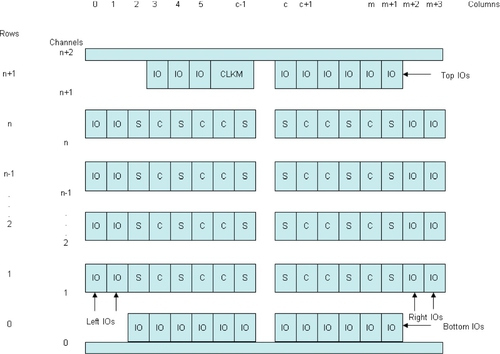
A typical FPGA will have hundreds or thousands of CLBs, of different types, on a single device allowing very complex devices to be implemented on a single chip and configured easily. Modern FPGAs have enough capacity to hold a number of complex processors on a single device. The layout of a typical FPGA (in CLB terms) is shown in Figure 2.5. As can be surmised from this schematic, the FPGA has a level of complexity possible that is orders of magnitude more than typical CPLD devices. With the advent of modern digital CMOS processes down to 45 nm or even 28 nm and beyond, the integration of millions of logical elements is now possible and to a speed unimaginable a decade previously—making extremely high-performance devices now possible (even into the realm of Gb/s data rates).
2.5 FPGA Design Techniques
When we design using a hardware description language (HDL), these logical expressions and functions need to be mapped onto the low level logic blocks on an FPGA. In order to do this, we need to carry out three specific functions:
1. Mapping: Logic functions mapped onto CLBs.
2. Placement: CLBs placed on FPGA.
3. Routing: Routed connections between CLBs.
It is clearly becoming impossible to design “by hand” using today’s complex designs; we therefore rely on synthesis software to turn our HDL design description into the logic functions that can be mapped onto the FPGA CLBs. This design flow is an iterative process including optimization and implies a complete design flow. This will be discussed later in this book in much more detail. One of the obvious aspects of FPGA design that must be considered, however, is that of the available resources.
2.6 Design Constraints using FPGAs
It can be very easy to produce unrealistic designs using an HDL if the target FPGA platform is not considered carefully. FPGAs obviously have a limited number of logic blocks and routing resources, and the designer has to consider this. The style of HDL code used by the designer should make the best use of resources, and this book will give examples of how that can be achieved. HDL code may be transferable between technologies, but may need rewriting for best results due to these constraints. For example, assumptions about the availability of resources may lead to a completely different style of design. An example would be a complex function that needed to be carried out numerous times. If the constraint was the raw performance, and the device was large enough, then simply duplicating that function in the hardware would enable maximum data rates to be achieved. On the other hand, if the device is very small and can only support a smaller number of functions, then it would be up to the designer to consider pipelining or resource sharing to enable the device to be programmed, but obviously this would be at the cost of raw performance. The constraints placed on the designer by the FPGA platform itself can therefore be a significant issue in the choice of device or development platform.
2.7 Development Kits and Boards
There are now a wide array of development kits to suit all levels of budget and performance requirements from the manufacturers themselves, or from third-party companies specializing in development kits and board design. With the FPGA manufacturers being proactive in providing design software on the web (often for free for noncommercial purposes), it has become much less of a hurdle for engineers to obtain access to both the design tools and the hardware to test out their concepts.
One of the major advantages with the modern development boards is that they tend to have an FPGA device that can generally handle almost all the major building blocks (processors, display drivers, network stacks) even on a relatively low-end device. The beauty of the boards too is that with the development of multiple layer PCB designs, most of the common interface elements can also be integrated on a very small board. With both Xilinx and Altera supporting credit card sized boards, these are well within the reach of students and engineers on a very small budget. Mid-Range boards are also available for more lab based usage, such as the DE series of boards from Terasic, based around the Altera FPGA devices, starting with the credit card sized DE0-Nano, DE0 and continuing up in power and complexity. An excellent starter board, for example, is the DE0 board, which is slightly larger than its DE0 successor, but perhaps a little easier to use in terms of access to switches and plugs. This board has two 40-way GPIO (General Purpose Input Output) connectors for general interfacing, a VGA output, PS/2 input, Ethernet, USB, SD Card socket and a selection of LEDs, switches, and buttons. This board is shown in Figure 2.6. There is a series of boards available for the Xilinx FPGAs, with similar ranges of options with an example being the Nexsys 3TM board from Digilent® which has a similar range of IO capability to the Altera based boards. The Nexsys 3TM board is shown in Figure 2.7.


With such an extensive range of options and prices, it is now a matter of choice in many cases which platform to use. Each one will have its strengths and weaknesses, and the designer is able to select the device and board to develop their own design, taking into account their own requirements and constraints.
2.8 Summary
This chapter introduces the basic technology behind FPGAs and their development. The key design issues are highlighted and some of the important design techniques introduced. Later chapters in this book will develop these in more detail either from a detailed design perspective or from a methodology point of view.