Latches, Flip-Flops, and Registers
Abstract
There are different types of storage elements that will occur from different HDL code, and it is important to understand each of them, so that the correct one results when a design is synthesized. Often bugs in hardware happen due to misunderstanding about what effect a particular HDL construct (in VHDL or Verilog) will have on the resulting synthesized hardware. In this chapter we will introduce the three main types of storage elements that can be synthesized from VHDL or Verilog to an FPGA platform; which are latches, flip-flops and registers.
20.1 Introduction
There are different types of storage elements that will occur from different HDL code, and it is important to understand each of them, so that the correct one results when a design is synthesized. Often bugs in hardware happen due to misunderstandings about what effect a particular HDL construct (in VHDL or Verilog) will have on the resulting synthesized hardware. In this chapter, we will introduce the three main types of storage elements that can be synthesized from VHDL or Verilog to an FPGA platform: which are latches, flip-flops, and registers.
20.2 Latches
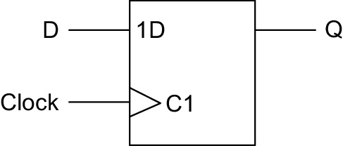
A latch can be simply defined as a level-sensitive memory device. In other words, the output depends purely on the value of the inputs. There are several different types of latch, the most common being the D latch and the SR latch. First consider a simple D latch as shown in Figure 20.1. In this type of latch, the output (Q) follows the input (D), but only when the Enable (En) is high. The full definition is in fact a level-sensitive D latch, and the assumption made in this book is that whenever we refer to a latch, it is always level sensitive. It is worth noting that latches are not particularly useful in FPGA design as they are obviously asynchronous and therefore can cause timing issues. In practice it is much better to use synchronous D-types, as will be introduced later in this chapter; however, it is worth looking at basic latches to see the differences.

The notation on the Enable signal (C1) and the Data input (1D) denotes that they are linked together. Also notice that the output Q is purely dependent on the level of D and the Enable. In other words, when the Enable is high, then Q = D. So, as previously stated, this is a level-sensitive latch.
The VHDL that represents this kind of level-sensitive D latch is shown here:
We can implement a very similar model using Verilog with the code given following this paragraph. In this case the Verilog uses the always statement to check for any changes on the enable or the d inputs and if enable (en) is high, then the output will also change.
This is an example of an incomplete if statement, where the condition if(en = 1) is given, but the else condition is not defined. Both d and en are in the sensitivity list and so this could be combinatorial, but due to the incomplete definition of en, then an implied latch occurs, that is, storage. This aspect of storage is important when we are developing models, particularly behavioral as in this case (i.e., the structure is not explicitly defined), as we may end up with latches in our design even though we think that we have created a model for a purely combinatorial circuit.
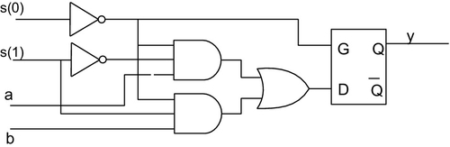
Other instances when this may occur are the incomplete definition of case statements. For example, consider this simple VHDL example:
In this statement, it is incomplete and so instead of a simple combinatorial circuit, a latch is therefore implied. The resulting synthesized circuit is shown in Figure 20.2.
Similar outcomes would happen if a Verilog case statement was incomplete:
In both cases it is important to ensure that all the states are defined to avoid this happening, and in Verilog this is done by using the default option in the case statement. Therefore, in our simple example, to ensure that all the possible values of s are covered, the default line will specify an output in those cases as shown here:
20.3 Flip-Flops
In contrast to the level-triggered latch, the flip-flop changes state when an edge occurs on an enable or a clock signal. This is the cornerstone of synchronous design, with an important building block being the D-type flip-flop, as shown in Figure 20.3. The output (Q) will take on the value of the input (D) on the rising edge of the clock signal. The triangle on the symbol denotes a clock signal and, in the absence of a circle (notation for active low), the definition is for a rising edge to activate the flip-flop.
The equivalent VHDL code is of the form shown as follows:
Notice that, in this case, d does not appear in the sensitivity list, as it is not required. The flip-flop will only do something when a rising edge occurs on the clock signal (clk). There are a number of different methods of describing this functionality, all of them equivalent. In this case, we have explicitly defined the clk signal in the sensitivity list.
An alternative method in VHDL would be to have no sensitivity list, but to add a wait on statement inside the process. The equivalent architecture would be as follows:
This could also be defined using a slightly different implementation of the wait statement, to wait for an event on clk and then check if it was high:
We have also perhaps used a more complex definition of the rising_edge function than is required (or may be available in all simulators or synthesis tools). The alternative simple method is to use the clock in the sensitivity list and then check that the value of clock is 1 for rising edge or 0 for falling edge. The equivalent VHDL for a rising edge D-type flip-flop is given. Notice that we have used the implicit sensitivity list (using a wait on clk statement) as opposed to the explicit sensitivity list, although we could use either interchangeably.
We can also implement this type of flip-flop using Verilog as shown here:
We can extend this basic model for a D-type to include an asynchronous set and reset function. If they are asynchronous, this means that they could happen whether there is a clock edge or not; therefore they need to be added to the sensitivity list of the model. The symbol for such a flip-flop, assuming active low set and reset, would be as shown in Figure 20.4.

The VHDL is extended from the simple dff model previously given to include the asynchronous set and reset as shown in the following:
As for the basic D type flip-flops, we could use a variation of the check for the clock edge, although due to the fact that we have three possible input state control variables (set, reset, and clk), it is not enough now to check whether the clock is high (for a rising edge flip-flop). It is necessary to check that the clock is high and that an event has occurred.
Notice that this model may cause interesting behavior when synthesized, as the reset will always be checked before the set and so there is a specific functionality that allows the concurrent setting of the set and reset variables, but the reset will take precedence.
We can also implement this behavior in a very similar fashion in Verilog as shown in the following listing:
Finally, when considering the use of transitions between 0 and 1, there are issues with synthesis and simulation when using the different approaches. For example, with the standard logic package (std_logic variables), the transitions are strictly defined and so we may have the case of high impedance or “don’t care” states occurring during a transition. This is where the rising_edge function and its opposite, the falling_edge function, are useful as they simplify all these options into a single function that handles all the possible transition states cleanly.
It is generally best, therefore, to use the rising_edge or falling_edge functions in VHDL (and posed and negedge in Verilog) wherever possible to ensure consistent and interoperable functionality of models.
It is also worth considering a synchronous set or reset function, so that the clock will be the only edge that is considered. The only caveat with this type of approach is that the set and reset signals should be checked immediately following the clock edge to make sure that concurrent edges on the set or reset signals have not occurred.
20.4 Registers
Registers use a bank of flip-flops to load and store data in a bus. The difference between a basic flip-flop and a register is that, while there is a data input, clock and usually a reset (or clear), there is also a load signal that defines whether the data on the input is to be loaded onto the register or not. The VHDL code for an example 8-bit register would be as follows:
This can also use a more indented form of if-then-else structure to separate the check on the clk and the load values as shown here:
Notice that although there are four inputs (clk, nrst, load, and d), only clk and nrst are included in the process sensitivity list. If load and d change, then the process will ignore these changes until the clk rising edge or nrst goes low. If the load is not used, then the register will load the data on every clock rising edge unless the reset is low. This can be useful in applications such as pipelining, where efficiency is paramount. The VHDL for this slightly simpler register is given here:
In a similar manner we can write a register model with an input d, load, and nrst control signals, with a clock input and the output q. In this case we use the posedge (positive edge) of the clock and the nest variable as the sensitivity list to the always block.
20.5 Summary
In this chapter, the basic type of latch and register have been introduced and examples given. This is a fundamental building block of synchronous digital systems and is the basis of RTL (Register Transfer Logic) design with VHDL or Verilog.