Synthesis
Abstract
This chapter introduces the key concept for modern FPGA design of synthesis. This process is the translation of a behavioral hardware description language representation into the low level bits that are programmed onto the hardware device. This chapter will review some of the design trade-offs commonly made between power, speed and area to ensure the design is functionally correct, and also optimized in the manner the designer requires.
6.1 Introduction
The original intention of hardware description languages was to have a design specification language for digital circuits. The main goal of the work was to have a design representation that could be simulated to test whether the specification was fit for purpose. When VHDL was standardized as IEEE Standard 1076, the broader application of VHDL for not just simulation but as an integral part of the hardware design flow became possible.
The original method of designing digital circuits was primarily through the development of schematic based designs, using gate libraries to effectively generate RTL netlists directly from the schematics. This is clearly a reasonable technique when the designs are relatively small, but it quickly becomes apparent that for designs of any size this approach is simply not realistic for modern FPGAs that require millions of gates.
EDA companies realized fairly early on in the HDL development process that if there was a standard language that could represent a data flow and a control flow, then the potential existed for automatically generating the gate level HDL from a higher level description, and RTL was the obvious place to start. RTL (Register Transfer Logic) has the advantage of representing the data flow and control flow directly, and can be mapped easily onto standard gate level logic. The resulting synthesis software (such as the Design Compiler from Synopsys) quickly established an important role in the digital design flow for both ASIC and FPGA designs and has in fact proved to be the driving force in the explosion of productivity of digital designers. The modern high density designs would not be possible without RTL synthesis.
For these reasons, modern day designers often simplify RTL synthesis to just “synthesis.” However, this is not the whole story. As designs have continued to become more complex, there has been an ever-increasing push to behavioral synthesis; however, there is not the same support from the EDA industry for behavioral synthesis software.
6.1.1 HDL Supported in RTL Synthesis
While VHDL is standardized, synthesis is not, so the VHDL that can be synthesized is a subset of the complete VHDL language. Another common problem for designers is the fact that different synthesis software packages will give different output results for the same input VHDL, even to the extent that some will synthesize and some will not under certain conditions. This also applies in equal measure to Verilog models, where various constructs will be not be able to be synthesized. Some of these are now discussed in the remainder of this chapter.
There are two types of unsupported elements in VHDL:
• those that will cause a synthesis failure;
• those that are just ignored.
The failure elements are in many respects easier to manage as the synthesis software will provide an error message. It is the ignored elements that can be more insidious as they can obviously leave errors in the synthesized design that may not be picked up until the hardware is tested.
Initial conditions
VHDL supports the initial condition being set for signals and variables; however, this is not physically realized. In practice the initial conditions in the synthesized design are random and so in a practical design a reset condition should always be defined using an external reset pin. This is because, during synthesis, the initial conditions are ignored.
Concurrent edges
It is common to use a clock edge as a trigger for a model, so a simple VHDL model may have a process to wait for the rising edge of a clock.
Or in a similar way:
What is NOT valid is to have more than one rising edge as the trigger condition, as this would fail the synthesis.
6.2 Numeric Types
Synthesis is only supported for numbers that have a finite range. For example, an integer type with an undefined range (infinite) is not supported by synthesis software. In general terms it is often required that designers specify the range of integers and other integer based numbers prior to synthesis (such as signed or unsigned). This can be a subtle restriction as vectors that have a number as the index must have this number defined in advance, so busses cannot be of a variable size. Floating point (real) numbers are generally not supported by synthesis software tools, as they do not have floating point libraries defined.
6.3 Wait Statements
Wait statements are only supported if the wait is of the form of an implied sensitivity list and a specific value. So, if the statement is something like:
then this is supported for synthesis. If the wait statement is dependent on a specific time delay then this is NOT supported for synthesis. For example, a statement in VHDL such as this is not supported:
6.4 Assertions
Assertions in any form are ignored by the synthesis software.
6.5 Loops
The FOR loop is a special case of the general loop mechanism in VHDL and synthesis requires that the range of the loop must be defined as a static value, globally. This means that you cannot use variables to define the range of the FOR loop on the fly for synthesis. If a while loop is implemented, then there has to be a wait statement in the loop somewhere; otherwise, it becomes a potentially infinite loop.
6.6 Some Interesting Cases Where Synthesis May Fail
Unfortunately, there are differences between synthesis software packages and so care must be taken to ensure interoperability between packages, particularly in multiteam designs or when using third-party VHDL cores. The cores may have been synthesized using software different from the one you are using in your design flow, so the advertised synthesizable core may not always be synthesizable for you, in your design flow.
Because of this, it is usually a good idea to keep the VHDL as generic as possible and avoid using tricks of a particular package if you plan to deliver IP cores or use different tools. This may lead to slightly less compact VHDL, but the reliability of the VHDL will be greater, and potential problems (which could cause significant delays later in the design process, particularly in an integration phase) can be avoided.
One case is the use of different trigger variables in a process. For example, if there is a clock and a reset signal, or a clock and an enable signal, it is tempting to combine the logic into one expression such as:
However, in some synthesis software this would cause an error. It is always preferable to separate these variables into nested if statements for three reasons:
1. The code will be more readable.
2. The chance of undefined logic states is reduced.
3. The synthesis software will not have a problem with your VHDL!
6.7 What Is Being Synthesized?
6.7.1 Overall Design Structure
The basic approach for synthesizing digital circuits is to consider every design block as a combination of a controller and a data path. The controller is generally a finite state machine (FSM), clocked, and the data path is usually combinatorial logic, but there may also be storage in there and so a clock may also be required. The basic outline is shown in Figure 6.1.
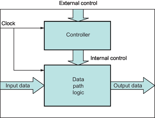
6.7.2 Controller
The controller is producing the control signals for the data path logic and may also have external control signals, so there are both internal and external control signals in the general case. As this is a FSM, the design is synchronous and therefore is clocked and will generally have a reset condition.
The controller can be represented using a state diagram or bubble diagram. This shows each individual state and all the transitions between the states. The controller can be of two basic types: Moore (where the output of the state machine is purely dependent on the state variables) and Mealy (where the output can depend on the current state variable values AND the input values). The behavior of the state machine is represented by the state diagram (also sometimes called a state chart) as shown in Figure 6.2.
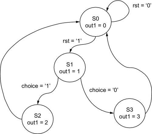
The technique for modeling finite state machines will be covered later in this book, but the key elements to remember are that, as this is a finite state machine, there are a finite number of states, and hence the number of storage elements (D types) is implicit in this definition. Also, the VHDL allows the definition of the state names as an enumerated type, which makes the VHDL readable, easy to understand and also easily synthesizable.
For example, take a simple example of a 2-state machine, where the states are called ON and OFF. If the onoff signal is low then the machine will be OFF and if the onoff switch is high, then the state machine will go into the ON state.
To implement this simple state machine in VHDL, we can use a new type to represent the states:
Notice that in the FSM VHDL we have defined both the current and the next state. The main part of the FSM can be easily implemented using a case statement in VHDL within a process that waits for changes in both the current_state signal and any external variables or control signals.
Elsewhere in the architecture, the current_state needs to be assigned to the next state as follows:
If we were to do something similar using Verilog, then the first step of defining a new type would be to specify the state names as defined below:
This is obviously a very simple example with only two states, requiring just one bit (4 states would require 2 bits, 8 states 3 and so on).
Using this definition, the state variables can then be defined using a simple register, and again only one bit is required for that:
So, the current state and the next state variables have been defined, and the next step is to define the state machine itself. We have several methods to implement this; however, if we stick to the use of a case statement, then the following code would demonstrate the correct behavior:
As with the VHDL example, the transition to the next state needs to be handled in a synchronous manner, and in Verilog this could be using the rising edge of the clock once again:
6.7.3 Data Path
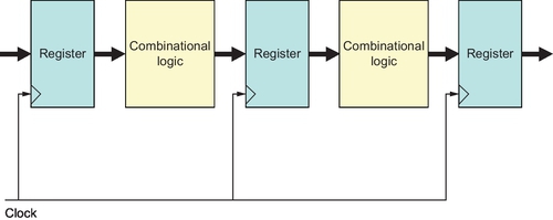
The data path logic is the logic (as the name suggests) to process the input data and generate the correct output data. The functionality of the data path logic will usually be divided into blocks and this offers the possibility of optimization for speed or area. For example, if area is not an issue, but speed is the primary concern, then a large design could be constructed to generate the output in potentially a single clock cycle. If the area is not an issue, but throughput is required, then pipelining could be used to maximize the overall data rates, although the individual latency may be high. Finally, if area is the critical factor, then single functional blocks can be used and registers used to store intermediate values and the same function applied repeatedly. Clearly this will be a lot slower, but potentially take a lot less space.
In the basic data path model there are blocks of combinational logic separated by registers. Clearly there are options for optimizing the data flow by considering how best to move the data between the registers for speed or area optimization.
It is important to ensure that some simple rules are followed to ensure robust synthesis. The first is to make sure that each signal in the combinational block is defined for every cycle; in other words it is important not to leave undefined branches in case or if statements. If this occurs, then a memory latch is inferred and therefore a latch will be synthesized and as this is not linked to the global clock, unpredictable behavior can result.
6.8 Summary
This chapter has introduced the concept of synthesis, both from a designer’s point of view and also the implications of using certain types of VHDL with the intention of synthesizing it. The assumptions and limitations of the various approaches have been described and some sensible practical approaches to obtaining more robust designs defined.