ALU Functions
Abstract
A central part of microprocessors is the ALU (Arithmetic Logic Unit). This block in a processor takes a number of inputs from registers and, as its name suggests, carries out either logic functions (such as NOT, AND, OR, and XOR) on the inputs, or arithmetic functions (addition or subtraction as a minimum), although it must be noted that these will be integer (or fixed point potentially) only and not floating point. This chapter of the book will describe how these types of low level logic and arithmetic functions can be implemented in VHDL and Verilog.
21.1 Introduction
A central part of microprocessors is the ALU (Arithmetic Logic Unit). This block in a processor takes a number of inputs from registers and as its name suggests carries out either logic functions (such as NOT, AND, OR, and XOR) on the inputs, or arithmetic functions (addition or subtraction at a minimum), although it must be noted that these will be integer (or fixed point, potentially) and not floating point. This chapter of the book will describe how these types of low-level logic and arithmetic functions can be implemented in VHDL and Verilog. In this chapter, in some cases we have used bit and in other std_logic, both of which are valid. In practice, most designers will use the more complete definition in std_logic (and the vector extension std_logic_vector); however, both may be used. In the case of std_logic, the IEEE library must be included.
21.2 Logic Functions in VHDL
If we consider a simple inverter in VHDL, we can develop a single inverter which takes a single input bit, inverts it and applies this to the output bit. This simple VHDL is shown as follows:
Clearly the inputs and output are defined as single std_logic pins, with direction in and out, respectively. The logic equation is also intuitive and straightforward to implement. We can extend this to be applicable to n bit logic busses by changing the entity (the architecture remains the same) and simply assigning the input and outputs the type std_logic_vector instead of std_logic, as follows:
As can be seen from the VHDL, we have defined a specific 16-bit bus in this example, and while this is generally fine for processor design with a fixed architecture, sometimes it is useful to have a more general case, with a configurable bus width. In this case we can modify the entity again to make the bus width a parameter of the model, which highlights the power of using generic parameters in VHDL.
We can of course create separate models of this form to implement multiple logic functions, but we can also create a compact multiple function logic block by using a set of configuration pins to define which function is required. If we define a general logic block that has 2 n-bit inputs (A and B), a control bus (S) and an n-bit output (Q), then by setting the 2-bit control word (S) we can select an appropriate logic function according to the following table:
Clearly we could define more functions, and this would require more bits for the select function (S) which could also be defined using a generic, but this limited set of functions demonstrates the principle involved. We can define a modified entity as shown:
Now, depending on the value of the input word (S), the appropriate logic function can be selected. We can use the case statement introduced in Chapter 3, A VHDL Primer to define each state of S and which function will be carried out in a very compact form of VHDL:
Clearly this is an efficient and compact method of defining the combinatorial logic for each state of the control word (S), but great care must be taken to assign values for every combination to avoid inadvertent latches being introduced into the logic when synthesized. To avoid this, a synchronous equivalent could also be implemented that only applied the logic function on the clock edge specified.
In this example, all of the possible combinations are specified; however, in order to avoid possible inadvertent latches being introduced, it would be good practice to use a “when others” statement to cover all the unused cases.
21.2.1 1-bit Adder
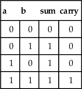
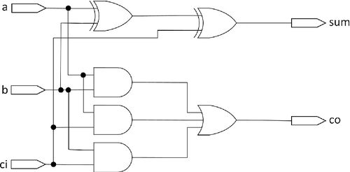
The arithmetic heart of an ALU is the addition function (Adder). This starts from a simple 1-bit adder and is then extended to multiple bits, to whatever size addition function is required in the ALU. The basic design of a 1-bit adder is to take two logic inputs (a and b) and produce a sum and carry output according to the following truth table:
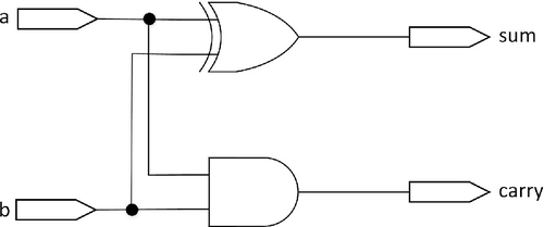
This can be implemented using simple logic with a 2 input AND gate for the carry, and a 2 input XOR gate for the sum function, as shown in Figure 21.1.
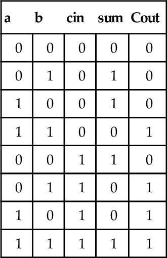
This function has a carry out (carry), but no carry in, so to extend this to multiple bit addition, we need to implement a carry in function (cin) and a carry out (cout) as follows:
With an equivalent logic function as shown in Figure 21.2:
This can be implemented using standard VHDL logic functions with bit inputs and outputs as follows. First, define the entity with the input and output ports defined using bit types:
Then the architecture can use the standard built-in logic functions in a dataflow type of model, where logic equations are used to define the behavior, without any delays implemented in the model.
This model is now a simple building block that we can use to create multiple bit adders structurally by linking a number of these models together.
21.3 Structural n-Bit Addition
Using the simple 1-bit full adder defined previously, it is a simple matter to create a multiple bit full adder using this model as a building block. As an example, to create a 4-bit adder, with a single bit carry in and single bit carry out, we can define a VHDL model as shown here:
This can obviously be extended to multiple bits by repeating the component use in the architecture for as many bits as are required.
21.4 Logic Functions in Verilog
If we consider a simple inverter in Verilog, this takes a single input bit, inverts it and applies this to the output bit. This simple Verilog code is shown here:
Clearly the inputs and output are defined as single std_logic pins, with direction in and out respectively. The logic equation is also intuitive and straightforward to implement. We can extend this to be applicable to n bit logic busses by changing the inputs and outputs (the architecture remains the same) into bus types as follows:
As can be seen from the Verilog, we have defined a specific 16-bit bus in this example, and while this is generally fine for processor design with a fixed architecture, sometimes it is useful to have a more general case, with a configurable bus width. In this case we can modify the Verilog again to make the bus width a parameter of the model:
We can of course create separate models of this form to implement multiple logic functions, but we can also create a compact multiple function logic block by using a set of configuration pins to define which function is required, as we did in the case for the VHDL. Clearly we could define more functions, and this would require more bits for the select function (S), but this limited set of functions demonstrates the principle involved.
Now, depending on the value of the input word (S), the appropriate logic function can be selected. We can use the case statement introduced in Chapter 3 of this book to define each state of S and which function will be carried out in a very compact form. As in the VHDL case, this is an efficient and compact method of defining the combinatorial logic for each state of the control word (S), but great care must be taken to assign values for every combination to avoid inadvertent latches being introduced into the logic when synthesized.
21.5 Configurable n-Bit Addition
While the structural approach is useful, it is clearly cumbersome and difficult to configure easily. A more sensible approach is to add a generic (parameter) to the model to enable the number of bits to be customized. For example, if we define an entity to add two logic vectors (as opposed to bit vectors used previously), the entity will look something like this:
As can be seen from this entity, we have a new parameter, top, which defines the size of the input vectors (a and b) and the output sum (cout). We can then use the same original logic equations that we defined for the initial 1-bit adder and use more behavioral VHDL to create a much more readable model:
This architecture shows how a single process (with sensitivity list a,b,cin) is used to encapsulate the addition. The process is activated when a,b or cin changes. A for loop is used to calculate a temporary sum (tempsum) that increments each time around the loop if required and the final value is assigned to the output sum. Also, a stage by stage carry is calculated and used each time around the loop. After the final loop, the value of carry is used to become the final carry out.
21.6 Two’s Complement
An integral part of subtraction in logic systems is the use of two’s complement. This enables us to execute a subtraction function using only an adder rather than requiring a separate subtraction function. Two’s complement is an extension to the basic ones’ complement (or basic inversion of bits) previously considered.
If we consider an unsigned number system based on 4 bits, then the range of the numbers is 0 to 15 (0000 to 1111). If we consider a signed system, however, the most significant bit (MSB) is considered to be the sign (+ or −) of the number system and therefore the range of numbers with 4 bits will instead be from −8 to +7. The method of conversion from positive to negative number in binary logic is a simple two-stage process of first inverting all the bits and then adding 1 to the result.
Consider an example. Take a number 00112. In signed number form, the MSB is 0, so the number is positive and the lower three bits 011 can be directly translated into decimal 3. To get the two’s complement (−3), we first invert all the bits to get 1100, and then add a single bit to get the final two’s complement value 1101. To check that this is indeed the inverse in binary, simple add the number 0011 to its two’s complement 1101 and the result should be 0000.
In a signed system the range of numbers is − (2N − 1) to + (2N − 1 − 1) whereas in the unsigned system the range is defined by 0 to + (2N − 1). The signed system allows both positive and negative numbers; however, the maximum magnitude is effectively half the magnitude of the unsigned system.
This function can be implemented simply in VHDL using the following model:
As can be seen from the VHDL, we operate using logic functions first (NOT) and then convert to unsigned to utilize the addition function (inv + 1), and finally convert the result back into a std_logic_vector type. Also notice that the generic n allows this model to be configured for any data size. In this example, the test bench is used to check that the function is operating correctly by using two test circuits back to back, inverting and re-inverting the input word and checking that the function returns the same value. While this does not guarantee correct operation (the same bug could be present in both transforms!), it is a simple quick check that is very useful and makes generation of test data and checks very easy, as the input and final output signal check can be XORed to check for differences.
21.7 Summary
This chapter has introduced the key elements required in an Arithmetic and Logic Unit of a processor. Whether the designer needs to implement a complete ALU from scratch, or just to understand the behavior of an existing architecture, these functions are very useful in analyzing the behavior of ALUs and processors.