
Digital Filters
Abstract
An important part of digital or computing systems that interface to the “real /world” of sensors and analog interfaces is the ability to process sampled data in the digital domain. This is often called Sampled Data Systems (SDS) or defined as operating in the Z-domain. Most engineers are familiar with the operation of filters in the Laplace or S-domain where a continuous function defines the characteristics of the filter and this is the digital domain equivalent to that.
9.1 Introduction
An important part of digital or computing systems that interface to the “real/world” of sensors and analog interfaces is the ability to process sampled data in the digital domain. This is often called Sampled Data Systems (SDS) or defined as operating in the Z-domain. Most engineers are familiar with the operation of filters in the Laplace or S-domain where a continuous function defines the characteristics of the filter and this is the digital domain equivalent to that.
For example, consider a simple RC circuit in the analog domain, which is designed to be a low pass filter, as shown in Figure 9.1.
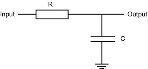
This has a low pass filter behavior and can be represented mathematically using the continuous Laplace (or S-domain) notation:
This function is a low pass filter because the Laplace operator s is equivalent to jω, where ω = 2πf (with f being the frequency). If f is zero (the d.c. condition), then the gain will be 1, but if the value of sRC is equal to 1, then the gain will be 0.5. This in dB is −3 dB and is the classical low pass filter cut-off frequency.
In the digital domain, the s operation is replaced by Z. Z−1 is equivalent in a practical sense to a delay operator, and similar functions to the Laplace filter equations can be constructed for the digital, or Z domain, equivalent.
There are a number of design techniques, many beyond the scope of this book (if the reader requires a more detailed introduction to the realm of digital filters, Cunningham’s Digital Filtering: An Introduction is a useful starting point); however, it is useful to introduce some of the basic techniques used in practice and illustrate them with examples.
The remainder of this chapter will cover the introduction to the basic techniques and then demonstrate how these can be implemented using VHDL and Verilog on FPGAs.
9.2 Converting S Domain to Z Domain
The method of converting an S domain equation for a filter to its equivalent Z domain expression uses the bilinear transform. This is a standard method for expressing the S-domain equation in the Z-domain. The basic approach is to replace each instance of s with its equivalent Z domain notation and then rearrange into the most convenient form. The transform is called bilinear as both the numerator and denominator of the expression are linear in terms of z.
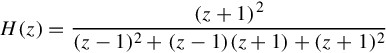
If we take a simple example of a basic second order filter we can show how this is translated into the equivalent Z domain form:
In order to get the function H(s) in its Z-domain equivalent, replace each occurrence of s with the expression for s in terms of z shown in Equation (9.2), giving:


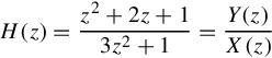
Now, the term H(z) is really the output Y (z) over the input X(z) and we can use this to express the Z domain equation in terms of the input and output:
This can then be turned into a sequence expression using delays (z is one delay, z2 is two delays and so on) with the following result:
This is useful because we are now expressing the Z domain equation in terms of delay terms, and the final step is to express the value of y(n) (the current output) in terms of past elements by reducing the delays accordingly (by 2 in this case):
The final design note at this point is to make sure that the design frequency is correct, for example the low pass cut-off frequency. The frequencies are different between the S and Z domain models, even after the bilinear transformation, and in fact the desired digital domain frequency must be translated into the equivalent s domain frequency using a technique called prewarping. This simple step translates the frequency from one domain to the other using the following expression:
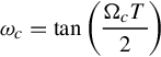
where Ωc is the digital domain frequency, T is the sampling period of the Z domain system and ωc is the resulting frequency for the analog domain calculations.
Once we have obtained our Z domain expressions, how do we turn this into practical designs? The next section will explain how this can be achieved in VHDL.
9.3 Implementing Z Domain Functions in VHDL
9.3.1 Introduction
Z domain functions are essentially digital in the time domain as they are discrete and sampled. The functions are also discrete in the amplitude axis, as the variables or signals are defined using a fixed number of bits in a real hardware system; whether this is integer, signed, fixed point, or floating point, there is always a finite resolution to the signals. For the remainder of this chapter, signed arithmetic is assumed for simplicity and ease of understanding. This also essentially defines the number of bits to be used in the system. If we have 8 bits, the resolution is 1 bit and the range is −128 to +127.
9.3.2 Gain Block
The first main Z domain block is a simple gain block. This requires a single signed input, a single signed output and a parameter for the gain. This could be an integer or also a signed value. The VHDL model for a simple Z domain gain block is given as:
We can test this with a simple testbench that ramps up the input and we can observe the output being changed in turn:
Clearly, this model has no error checking or range checking and the obvious problem with this type of approach is that of overflow. For example, if we multiply the input (64) by a gain of 2, we will get 128, but that is the sign bit, and so the result will show −128! This is an obvious problem with this simplistic model and care must be taken to ensure that adequate checking takes place in the model.
9.3.3 Sum and Difference
Using this same basic approach, we can create sum and difference models which are also essential building blocks for a Z domain system. The sum model VHDL is shown here:
Despite the potential for problems with overflow, both of the models shown have the internal variable that is twice the number of bits required, and so this can take care of any possible overflow internal to the model, and in fact checking could take place prior to the final assignment of the output to ensure the data is correct. The difference model is almost identical to the sum model except that the difference of zin1 and zin2 is computed.
9.3.4 Division Model
A useful model for scaling numbers simply in the Z domain is the division by 2 model. This model simply shifts the current value in the input to the right by one bit, hence giving a division by 2. The model could easily be extended to shift right by any number of bits, but this simple version is very useful by itself. The VHDL for the model relies on the logical shift right operator (SRL) which not only shifts the bits right (losing the least significant bit) but adds a zero at the most significant bit. The resulting VHDL is shown for this specific function:
The unit shift can be replaced by any integer number to give a shift of a specific number of bits. For example, to shift right by 3 bits (effectively a divide by 8) would have the following VHDL:
The complete division by 2 model is given here:
In order to test the model a simple test circuit that ramps up the input is used and this is given as follows:
The behavior of the model is useful to review. If the input is X03 (Decimal 3), binary 00000011 and the number is right shifted by one, then the resulting binary number will be 00000001 (X01 or decimal 1); in other words this operation always rounds down. This has obvious implications for potential loss of accuracy and the operation is skewed downward, which has, again, implications for how numbers will be treated using this operator in a more complex circuit.
9.3.5 Unit Delay Model
The final basic model is the unit delay model (zdelay). This has a clock input (clk) using a std_logic signal to make it simple to interface to standard digital controls. The output is simply a one clock cycle delayed version of the input.
Notice that the output zout is initialized to all zeros for the initial state; otherwise don’t care conditions can result that propagate across the complete model.
9.4 Basic Low Pass Filter Model
We can put these elements together in simple models that implement basic filter blocks in any configuration we require, as always taking care to ensure that overflow errors are checked for in practice.
To demonstrate this, we can implement a simple low pass filter using the basic block diagram shown in Figure 9.2.
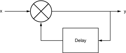
We can create a simple test circuit that uses the individual models we have already shown for the sum and delay blocks and apply a step change and observe the response of the filter to this stimulus. Clearly, in this case, with unity gain the filter exhibits positive feedback and so to ensure the correct behavior we use the divide by 2 model zdiv2 in both the inputs to the sum block to ensure gain of 0.5 on both. These are not shown in the figure. The resulting VHDL model is shown in the following code (note the use of the zdiv2 model):
The test circuit applies a step change of X00 to X0F after 10 μs, and this results in the filter response. We can show this graphically in Figure 9.3 with the output in both hexadecimal and analog form for illustration.
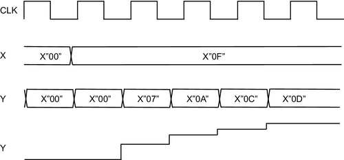
It is interesting to note the effect of using the zdiv2 function on the results. With the input of 0F (binary 00001111) we lose the LSB when we divide by 2, giving the resulting input to the sum block of 00000111 (7) which added together with the division of the output gives a total of 14 as the maximum possible output from the filter. In fact, the filter gives an output of X0D or binary 00001101, which is two down from the theoretical maximum of X0F and this highlights the practical difficulties when using a coarse approximation technique for numerical work rather than a fixed or floating point method. On the other hand, it is clearly a simple and effective method of implementing a basic filter in VHDL.
Later in this book, the use of fixed and floating point numbers are discussed, as is the use of multiplication for more exact calculations and for practical filter design; where higher accuracy is required, then it is likely that both these methods would be used. There may be situations, however, where it is simply not possible to use these advanced techniques, particularly a problem when space is at a premium on the FPGA and, in these cases, the simple approach described in this chapter will be required.
There are numerous texts on more advanced topics in digital filter design, and these are beyond the scope of this book, but it is useful to introduce some key concepts at this stage of the two main types of digital filter in common usage today. These are the recursive (or Infinite Impulse Response, IIR) filters and nonrecursive (or Finite Impulse Response, FIR) filters.
9.5 Implementing Z Domain Functions in Verilog
9.5.1 Gain Block
The first main Z domain block is a simple gain block. This requires a single signed input, a single signed output and a parameter for the gain. This could be an integer or also a signed value. The Verilog model for a simple Z domain gain block is given as follows:
Clearly, as with the VHDL model, this model has no error checking or range checking and the obvious problem with this type of approach is that of overflow. For example, in an 8-bit model, if we multiply the input (64) by a gain of 2, we will get 128, but that is the sign bit, and so the result will show −127! This is an obvious problem with this simplistic model and care must be taken to ensure that adequate checking takes place in the model.
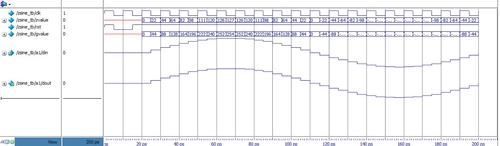
We can test the model by using a simple test bench that has a lookup table to generate a sine wave which will go from −127 to +127, and the gain can be varied using the parameter of the gain block. The number of bits in the gain block defaults to the parameter n value (default is 8) and the output is 2 * n. This makes the assumption that the gain will be no larger than the input value maximum, and this should obviously be checked thoroughly in a practical model to avoid the possibility of overflow errors occurring. The test bench Verilog is shown here:
When the model was simulated with a gain of 2, n = 8, the output values can be seen in Figure 9.4 to exactly double the input values, and as the gain block sensitivity is on the input, the change is immediate (unlike a synchronous model which would only change on the clock edge). The waveforms are shown in Figure 9.4.
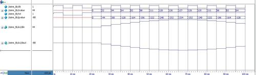
When the gain is reversed to − 2, the output has the same amplitude as before, but now the output is inverted, and this can easily be seen to be correct in the waveform diagram in Figure 9.5.
9.5.2 Sum and Difference
Using this same basic approach, we can create sum and difference models which are also essential building blocks for a Z domain system. The sum model Verilog is shown here:
Despite the potential for problems with overflow, both of the models shown have the internal variable that is twice the number of bits required, and so this can take care of any possible overflow internal to the model, and in fact checking could take place prior to the final assignment of the output to ensure the data is correct. The difference model is almost identical to the sum model except that the difference of din1 and din2 is computed.
9.5.3 Unit Delay Model
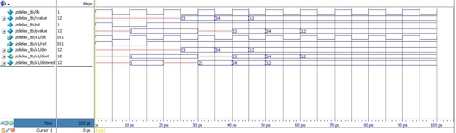
The final basic model is the unit delay model (zdelay). This has a clock input (clk) and a reset (rst) signal to make it simple to interface to standard digital controls. The output is simply a one clock cycle delayed version of the input.
Notice that the output dout is initialized to all zeros for the initial state, otherwise don’t care conditions can result that propagate across the complete model.
The model was tested using a basic test bench as shown below to illustrate how the simple delay operates:
The resulting behavior can clearly be seen in Figure 9.6.
Later in this book, the use of fixed and floating point numbers are discussed, as is the use of multiplication for more exact calculations and for practical filter design, where higher accuracy is required, it is likely that both these methods would be used. There may be situations, however, where it is simply not possible to use these advanced techniques, particularly a problem when space is at a premium on the FPGA; in these cases, the simple approach described in this chapter will be required.
There are numerous texts on more advanced topics in digital filter design, and these are beyond the scope of this book, but it is useful to introduce some key concepts at this stage of the two main types of digital filter in common usage today. These are the recursive (or Infinite Impulse Response, IIR) filters and nonrecursive (or Finite Impulse Response, FIR) filters.
9.6 Finite Impulse Response Filters
Finite impulse response (FIR) filters are characterized by the fact that they use only delayed versions of the input signal to filter the input to the output. For example, if we take the expression for a general FIR filter below, we can see that the output is a function of a series of delayed, scaled versions of the input:
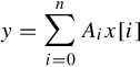
where Ai is the scale factor for the ith delayed version of the input. We can represent this graphically in the diagram shown in Figure 9.7. We can implement this model using the basic building blocks described in this chapter of gain, division, sums and delays to develop block based models for such filters. As noted in the previous section, it is important to ensure that for higher accuracy filters, fixed or floating point arithmetic is required and also the use of multipliers for added accuracy is preferable in most cases to that of simple gain and division blocks as described previously in this chapter.

9.7 Infinite Impulse Response Filters
Infinite impulse response (IIR) filters are characterized by the fact that they use delayed versions of the input signal and fed-back and delayed versions of the output signal to filter the input to the output. For example, if we take the expression for a general IIR filter below, we can see that the output is a function of a series of delayed, scaled versions of the input and output.
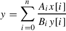
where Ai is the scale factor for the ith delayed version of the input and Bi is the scale factor for the ith delayed version of the output. This is obviously very similar to the FIR example previously given and can be built up using the same basic elements. If we consider the simple example earlier in this chapter, it can be seen that this is in fact a simple first order (single delay) IIR filter, with no delayed versions of the input and a single delayed version of the output.
9.8 Summary
This chapter has introduced the concepts of implementing basic digital filters and Z-domain functions in VHDL and Verilog and has given examples of both the building blocks and constructed filters for implementation on an FPGA platform. The general concepts of FIR and IIR filters have been introduced so that the reader can implement the topology and type of filter appropriate for their own application. A detailed treatise on filters is beyond the scope of this book and the reader is referred to one of the many digital filter design texts available for a more in-depth analysis of the topic.