High Speed Video Application
Abstract
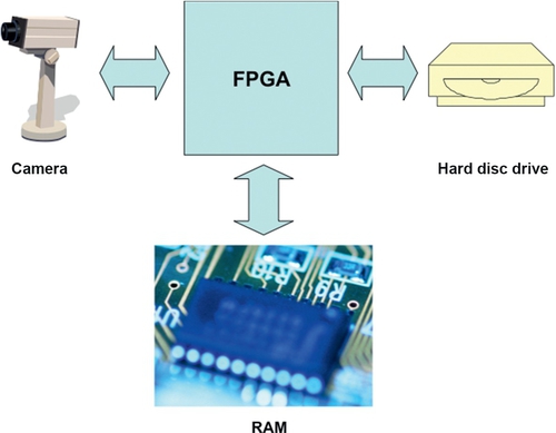
This application is designed to show how several high data rate applications can be handled using VHDL on FPGAs. The system consists of a high speed camera, processor core, disk drive interface, RAM interface and serial link to an external PC. The overall system has been chosen to illustrate how to move large amounts of data around quickly and efficiently. The outline of such a test application is shown in the figure below. As can be seen, there are several key aspects involved, but mainly it is about moving large amounts of data around a system quickly, efficiently, and reliably.
7.1 Introduction
This application is designed to show how several high data rate applications can be handled using VHDL on FPGAs. The system consists of a high-speed camera, processor core, disk drive interface, RAM interface, and serial link to an external PC. The overall system has been chosen to illustrate how to move large amounts of data around quickly and efficiently. The outline of such a test application is shown in the following figure. As can be seen, there are several key aspects involved, but mainly it is about moving large amounts of data around a system quickly, efficiently, and reliably.
The basic system is shown in outline form in Figure 7.1:
The key performance aspect of this system is in the three interfaces:
• FPGA to PC/Hard Disc Drive (HDD)
• FPGA to RAM
If we consider the basic camera performance criteria, we have four issues to consider:
• Frame rate
• Color specification
• Clip size
In this example, the resolution is defined as being 640 × 480 pixels, the color mode is 24-bit color (3 × 8 bit planes), the maximum frame rate is 100 per second and finally the basic clip size is anything up to 10 s.
What is not shown in the overview figure is the requirement for some basic control options (such as play, record, store) to allow the stored clips to be replayed using a standard VGA output (available on most FPGA development kits) or stored for long-term storage on a hard disc drive (or similar high capacity storage device). This could be handled separately using a PC interface, but that detail is beyond the scope of this basic system description.
7.2 The Camera Link Interface
7.2.1 Hardware Interface
There are a number of approaches for linking cameras for the high-speed transfer of data, with the two most common being USB (to PCs) and a standard Camera Link using LVDS serial data transmission. The LVDS (Low Voltage Differential Swing) system is a differential serial link that uses voltages of about 350 mV to transmit high-speed data with low noise and low power. Many FPGA development kits have a standard LVDS bus available and this means that the signals can be connected directly between the camera and the FPGA board to transfer data from the camera to the FPGA and hence to the storage (either RAM or HDD).
7.2.2 Data Rates
The actual data rate required is theoretically the resolution multiplied by the frame rate multiplied by the number of bits required for each pixel, which in this example would mean the following calculation:
which for the specification would mean a total data rate of:
This equates to a data rate of over 90 MB/s (megabytes per second) and as such is extremely fast for a practical application. Even if the FPGA could run at 100 MHz, the margin on such a system is pretty small.
7.2.3 The Bayer Pattern
Luckily, in practice, most camera systems do not use 24 bits in this raw fashion. Kodak has developed the Bayer pattern which is a technique whereby instead of requiring each pixel to have its own individual three color planes (requiring 24 bits in total), an array of color filters is placed over the camera sensor and this limits the requirement for data bits per pixel to a single 8-bit byte (with a known color filter in place). The Bayer pattern is repeated over the image in a fixed configuration to standardize this process. The Bayer pattern is shown in Figure 7.2.
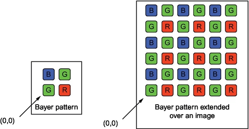
Clearly, using this approach, the required data rate can be divided by three and reduces to a more manageable 30 MB/s. Clearly, the disadvantage of this approach is that the resolution is reduced; however, most images can be reconstructed fairly readily using a method of interpolation which checks firstly which color the current pixel is (red, green, or blue, denoted by R, G or B respectively) and then takes an average of the neighboring pixels of the missing colors. For example, if the current pixel color is green, then the blue and red color of the current pixel is obtained by averaging the neighboring blue (2) and red (2) pixels, respectively.
7.2.4 Memory Requirements
Taking the use of Bayer patterns to reduce the sheer amount of data required into account, this means that the RAM requirements are still high; in this case for a 640 × 480 image size, this will require a memory size of:
Clearly, a large memory is going to be required for any significant memory storage and it is unlikely to be possible to store this on the FPGA itself. A more practical solution will be to use some RAM connected to the FPGA (or perhaps available on the development board itself). Options for the memory could include SDRAM or Flash memory. Both of these options will be discussed in detail later in the book; however, it is useful to consider the advantages and disadvantages of each approach in general. If we consider SDRAM (Synchronous Dynamic Random Access Memory), the key aspects of this type of memory to consider are:
• This type of DRAM (Dynamic RAM) relies on transistor capacitance on gates to store data.
• DRAM is much more compact than SRAM (Static RAM).
• DRAM cannot be synthesized; you need a separate DRAM chip.
• SDRAM requires a synchronization clock that is consistent with the rest of the hardware system (it is designed to operate with microprocessors).
• DRAM data must be refreshed as it is stored charge and decays after a certain time.
• DRAM is slower than SRAM.
Static RAM (SRAM) can be considered in a similar way to a ROM chip and it also has (differing) key aspects of behavior to consider:
• Memory cells are based on standard latches.
• SRAM is fast.
• SRAM is less compact than DRAM (or SDRAM).
• SRAM can be synthesized on an FPGA so is ideal for small, fast registers, or memory blocks.
Static RAM is essentially asynchronous, but can be modified to behave synchronously (as SDRAM is the synchronous equivalent of DRAM), and this is often called Synchronous RAM. Flash memory is useful to consider at this point, even though its operation is fundamentally different from the memory types considered thus far, simply because it is easy to use and is commonly available on many FPGA development boards. Flash memory is essentially a form of EEPROM (electrically programmable ROM) that can be used as a form of persistent RAM. Why persistent? In Flash memory, the device memory is retained even when the power is removed, so it is often used as a form of ROM, which makes it an interesting memory to use on FPGA systems as it could be used to store the FPGA program, but also used as a RAM storage (dynamically) for current data.
7.3 Getting Started
Now that the basic context of the design has been described and the basic specification firmed up, the first stage of the actual design can start. In practice, many of the individual blocks may exist in some form, but may need to be modified to fit the specific application requirements. However, generally speaking it is sensible to start with a top-down design methodology. What that means is that, based on the specification, a top level block can be designed that has the correct pin interface (although this may change as the design is refined) and an outline block structure that contains the functional blocks in the design. If we consider the design example in this part of the book a typical starting point will be a top level diagram showing the basic building blocks of the design and the overall interfaces. Some of the details will not be complete at this stage, but we can start to construct a top level design and we can fill in the details later as we go on with the details of each design block.
Figure 7.3 shows the outline top level design of the application.

The essential features of the design are captured in this sketch: the main functional blocks, the key interfaces and also notice that we have identified a system clock and reset that will propagate to all the individual functional blocks. Notice also that in the original design we did not specify the user input mechanism: that is, how does the user control the camera interface or store data? We have made a design decision at this point, which is to use a simple mouse and keyboard interface to provide the user control to the FPGA system. This allows a flexible approach, so in the first instance, we could use mouse keys or specific keys on the keyboard to initiate a record sequence, or playback, or store, but ultimately, depending on how complex we wish to make the design, it would be possible to design a simple user interface with buttons or similar user interface features, actually on the display to allow controls to drive the system.
7.4 Specifying the Interfaces
From the sketch shown in Figure 7.1 we can begin to identify the interface requirements for the top level design. First, we clearly need a clock and reset (active low), so keeping things simple (always a good strategy) we can define the clock pin as clk and the reset pin as nrst. These are standard logic connections, and so we will use the basic standard logic type defined in the IEEE std_logic library. This does not define any details about the actual implementation of the pins (5V or 3.3V or even 1V), but simply the number of logic levels in the model. The actual implementation is defined by the FPGA being used.
7.5 Defining the Top Level Design
For this design we must define a top level entity name, and also individual block names. It is always a good idea to use meaningful names (unless they become unmanageable, in which case acronyms can be helpful), and hierarchy can also help in keeping duplicate name problems to a minimum. For example, in this case, the design is for an image handler and storage interface, which is clearly a mouthful, so in this example, we will shorten it to IHSI (remember that VHDL is case insensitive). Each main block below this top level will then have the prefix ihsi_ to identify the block in the design. This also has the effect of keeping all the blocks grouped together in the same place alphabetically in the compiled library, which makes things easier to find. We can therefore produce the first initial top level entity for the complete application:
In Verilog this will become:
We can then identify each major block that requires an external interface and add the requisite connection points to the top level entity. It is worth remembering that at each stage of the design, we do not need to have every block defined completely to test other parts of the design. We can use behavioral models or even empty models to simply ensure that the interfaces are in place and then replace each empty block with a fully functional one. We can also start with behavioral models, replace with RTL models and finally even replace these with synthesized ones. Thus, a complete system can be tested piece by piece until all the blocks are in place.
7.6 System Block Definitions and Interfaces
7.6.1 Overall System Decomposition
In this specific application we have several important blocks with external interfaces including:
• Keyboard Controller (PS/2)
• Flash Memory
• VGA Output
• Camera Link
• PC Interface
We can take each of these interfaces in turn and specify the requisite interface connections required for the design.
7.6.2 Mouse and Keyboard Interfaces
The mouse and keyboard PS/2 interfaces are relatively easy. Each of these has a clock and a data connection and so for each we can define two pins as follows:
Keyboard: key_clk, key_data
In the general case, the PS/2 interface (to be covered in more detail in Part 3 of this book) allows both directions to be used (i.e., device to controller and vice versa), so these connections must be defined as INOUT std_logic connections in our top level entity.
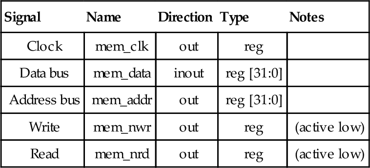
7.6.3 Memory Interface
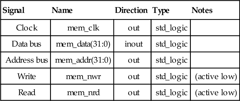
For the memory interface, we have two options. The first option is to define precisely the type of memory we are going to use in this application (RAM, Flash, EEROM, DRAM, SRAM) and produce a specific interface that will work for only that type of memory. Another approach is to consider that we will treat whatever type of memory we have as generic RAM internally, and to design a memory block that will interface to the actual memory—we will treat the memory interface as essentially a virtual RAM block. For the initial design, therefore, we can treat the memory as a simple synchronous RAM block that has a clock, data bus, address bus, and write and read signals. For this initial interface, therefore, we will require the following signals only in VHDL:
| Signal | Name | Direction | Type | Notes |
| Clock | mem_clk | out | std_logic | |
| Data bus | mem_data(31:0) | inout | std_logic | |
| Address bus | mem_addr(31:0) | out | std_logic | |
| Write | mem_nwr | out | std_logic | (active low) |
| Read | mem_nrd | out | std_logic | (active low) |
In Verilog, this will be almost identical, with the definition as follows:
More details on modeling the memory interface and dedicated memory itself is given in Chapter 11.
7.6.4 The Display Interface: VGA
For the VGA output (to be described later in this book in more detail) we require a specific definition of pins for the connection to the VGA connector on a development board or system. The first set of pins required in any VGA system is the clock and sync pins. The global VGA clock needs to be set to a specific frequency (depending on the monitor), such as 25 MHz, and this must be derived from the system clock on the FPGA board (say 100 MHz). The VGA clock pin is called the pixel clock and we can use the naming convention of vga_ as a prefix, followed by the functional name. So, for the pixel clock, the pin is named vga_out_pixel_clock. In addition to the clock, there are three synchronization signals required, the horizontal sync (vga_hsync), the vertical sync (vga_vsync), and the composite sync (vga_comp_sync). Finally, there is a blank pulse (vga_out_blank_z). The set of pins defined next are the three color data sets. VGA has three color planes (red, green, and blue), each with a definition of 8 bits, giving 24 bits in total. As has been described previously, these can be processed using a Bayer pattern, but when the final output pixel data is put together, all three planes require some output values to be set (even if they are all zero). We can define these pins as 8 bit vectors as follows:
or in Verilog:
This provides a complete definition of the VGA interface to the monitor from the system as a whole. More details of the VGA interface mechanism is given in Chapter 14.
7.7 The Camera Link Interface
The Camera Link standard has been devised to provide a generic 26-pin interface to a wide range of digital cameras and as such we can specify a standard interface at the top level of our design. Although the interface requires 26 pins, they are configured differentially, and so we can specify the basic interface functionally using only 11 pins. There is a clock pin, which we can define as camera_clk, and then four camera control lines defined as cc1 to cc4, respectively. Using the camera_ prefix, we can therefore name these as camera_cc1, camera_cc2, camera_cc3, and camera_cc4. There are two serial communication lines, serTFG (comms to frame grabber) and serTC (comms to camera), which we can name as camera_sertfg and camera_sertc, respectively. Finally, we have the four connection pins from the camera which will contain the data from the device and these are named camera_x0, camera_x1, camera_x2, and camera_x3. Clearly, the actual interface requires differential outputs, and so eventually an extra interface will be required to translate the simple form of interface defined here to the specific pins of the connector.
7.8 The PC Interface
The interface to the PC could be using either a standard serial interface such as USB (covered in Chapter 15) or using a direct interface to a hard disc drive (HDD).
The HDD interface offers a different challenge from the RAM memory interface discussed previously. There are numerous standards for interfacing to HDDs including the major two in current use IDE/AT and SCSI. SCSI (or Small Computers System Interface) is commonly used for high-speed drives and has been historically used extensively in Unix based systems. SCSI is a generic systems interface, and therefore it allows almost ANY type of device to be attached to the system (SCSI) bus.
The IDE/AT standard was devised for HDDs only and so has the advantage of being specifically designed for HDD interfaces. IDE (Intelligent Drive Electronics/AT Attachment) drives are generally slower, but significantly cheaper than SCSI drives and so PCs tend to use an IDE/ATA interface and higher end workstations will use SCSI drives instead.
In this context, the IDE/ATA drive is highly appropriate as the interface is much simpler than the SCSI interface, and therefore more practical in developing a prototype system. If a more advanced system is required, then clearly this can be changed later. The IDE approach is to have a number of master and slave devices on the bus (anyone who has looked inside a PC will recognize the need for setting a master/slave switch or jumper on a drive before installation of an extra or new HDD). A bus controller sets a series of registers with commands and the selected device on the chain will execute. It is worth noting that the bus will operate at the speed of the slowest device on the chain.
There are a total of 13 registers in the IDE/ATA configuration. These registers are divided into command block registers and control block registers. The command block registers are for sending commands to the device or for posting the status of the device. The control block registers are used for device control and for posting an alternate status. The full details of interfacing to an IDE/ATA device is beyond the scope of this book and is not used in this example.
The complexity of the IDE/ATA interface is such that it would probably take several thousand lines of VHDL to implement completely. If the performance requirements were such that it was essential, then the reader can find numerous sources of information to implement this design, including the ATA 6/UDMA100 specification.
An alternative approach is to use a standard interface such as USB with memory buffering and compression to manage the data storage issues, where the USB interface is discussed in detail in Part 3 of this book.
7.9 Summary
In summary, this chapter shows how a high-level specification can be practically decomposed into a series of manageable problems that may all have a relatively simple solution. The key to successful systems design is to decompose the design into blocks that have a definable core function. This can then be implemented directly in VHDL. The second aspect of the design is to analyze the boundaries.
A common phrase coined by systems designers is “problems migrate to the boundaries.” In other words, we can easily construct a VHDL design if we know the core functionality; however, getting the individual blocks to communicate successfully is often much harder. As a result, the designer often spends a lot of debug time in integrating a number of different functions together, and being forced to rewrite large sections of code to make that happen.
A useful approach to handling this specific problem is to create empty VHDL models that do not operate functionally, but do have the correct interfaces. These models can be tested with basic communications test data to ensure that the correct signals are in place, the data can be passed around the complete design at the required data rates, and that errors in signal names, directions, and types can be sorted out prior to developing the core VHDL.
This chapter provides a useful introduction to the process of modeling and designing complex systems using VHDL and Verilog. The general approach of thinking at a high level, without going too deeply into the details of each block, has been highlighted.