
Simple Embedded Processors
Abstract
This application example chapter concentrates on the key topic of integrating processors onto FPGA designs. This ranges from simple 8- bit microprocessors up to large IP processor cores that require an element of hardware-software co-design involved. This chapter will take the reader through the basics of implementing a behavioral based microprocessor for evaluation of algorithms, through to the practicalities of structurally correct models that can be synthesized and implemented on an FPGA.
8.1 Introduction
This application example chapter concentrates on the key topic of integrating processors onto FPGA designs. This ranges from simple 8-bit microprocessors up to large IP processor cores that require an element of hardware-software co-design involved. This chapter will take the reader through the basics of implementing a behavioral based microprocessor for evaluation of algorithms, through to the practicalities of structurally correct models that can be synthesized and implemented on an FPGA.
One of the major challenges facing hardware designers in the 21st century is the problem of hardware-software co-design. This has moved on from a basic partitioning mechanism based on standard hardware architectures to the current situation where the algorithm itself can be optimized at a compilation level for performance or power by implementing appropriately at different levels with hardware or software as required. This aspect suits FPGAs perfectly, as they can handle fixed hardware architecture that runs software compiled onto memory, they can implement optimal hardware running at much faster rates than a software equivalent could, and there is now the option of configurable hardware that can adapt to the changing requirements of a modified environment.
8.2 A Simple Embedded Processor
8.2.1 Embedded Processor Architecture
A useful example of an embedded processor is to consider a generic microcontroller in the context of an FPGA platform. Take a simple example of a generic 8-bit microcontroller as shown in Figure 8.1.
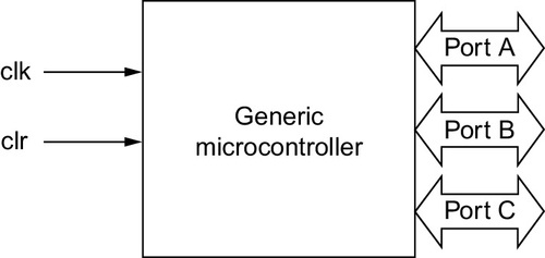
As can be seen from Figure 8.1, the microcontroller is a general-purpose microprocessor with a simple clock (clk) and reset (clr), and three 8-bit ports (A, B, and C). Within the microcontroller itself, there needs to be the following basic elements:
1. A control unit: this is required to manage the clock and reset of the processor, manage the data flow and instruction set flow, and control the port interfaces. There will also need to be a program counter (PC).
2. An ALU: a microcontroller will need to be able to carry out at least some rudimentary processing which is carried out in the ALU (Arithmetic Logic Unit).
3. An Address Bus.
4. A Data Bus.
5. Internal Registers.
6. An instruction decoder.
7. A ROM to hold the program.
While each of these individual elements (1-6) can be implemented simply enough using a standard FPGA, the ROM presents a specific difficulty. If we implement a ROM as a set of registers, then obviously this will be hugely inefficient in an FPGA architecture. However, in most modern FPGA platforms, there are blocks of RAM on the FPGA that can be accessed and it makes a lot of sense to design a RAM block for use as a ROM by initializing it with the ROM values on reset and then using that to run the program.
This aspect of the embedded core raises an important issue, which is the reduction in efficiency of using embedded rather than dedicated cores. There is usually a compromise involved and in this case it is that the ROM needs to be implemented in a different manner, in this case with a hardware penalty. The second issue is what type of memory core to use.
In an FPGA RAM, the memory can usually be organized in a variety of configurations to vary the depth (number of memory addresses required) and the width (width of the data bus). For example, a 512 address RAM block, with an 8-bit address width would be equivalent to a 256 address RAM block with a 16-bit address width.
If the equivalent microcontroller ROM is, say, 12 bits wide and 256, then we can use a 256 × 16 RAM block and ignore the top 4 bits. The resulting embedded microcontroller core architecture could be of the form shown in Figure 8.2.

8.2.2 Basic Instructions
When we program a microprocessor of any type, there are three different ways of representing the code that will run on the processor. These are machine code (1s and 0s), assembler (low level instructions such as LOAD, STORE), and high level code (such as C, Fortran, or Pascal). Regardless of the language used, the code will always be compiled or assembled into machine code at the lowest level for programming into memory. High level code (e.g., C) is compiled and assembler code is assembled (as the name suggests) into machine code for the specific platform.
Clearly a detailed explanation of a compiler is beyond the scope of this book, but the same basic process can be seen in an assembler and this is useful to discuss in this context. Every processor has a basic Instruction Set which is simply the list of functions that can be run in a program on the processor. Take the simple example of the following pseudocode expression:
In this example, we are taking the variable a and adding the integer value 2 to it, and then storing the result in the variable b. In a processor, the use of a variable is simply a memory location that stores the value, and so to load a variable we use an assembler command as follows:
What is actually going on here? Whenever we retrieve a variable value from memory, the implication is that we are going to put the value of the variable in the register called the accumulator (ACC). The command “LOAD a” could be expressed in natural language as “LOAD the value of the memory location denoted by a into the accumulator register ACC.”
The next stage of the process is to add the integer value 2 to the accumulator. This is a simple matter, as instead of an address, the value is simply added to the current value stored in the accumulator. The assembly language command would be something like:
Notice that we have used the x to denote a hexadecimal number. If we wished to add a variable, say called c, then the command would be the same, except that it would use the address c instead of the absolute number. The command would therefore be:
Now we have the value of a+2 stored in the accumulator register (ACC). This could be stored in a memory location, or put onto a port (e.g., PORT A). It is useful to notice that for a number we use the key character # to indicate that we are adding the value and not using the argument as the address. In the pseudocode example, we are storing the result of the addition in the variable called b, so the command would be something like this:
While this is superficially a complete definition of the instruction set requirements, there is one specific design detail that has to be decided on for any processor. This is the number of instructions and the data bus size. If we have a set of instructions with the number of instructions denoted by N, then the number of bits in the opcode (n) must conform to the following rule:
In other words, the number of bits provides the number of unique different codes that can be defined, and this defines the size of the instruction set possible. For example, if n = 3, then with 3 bits there are 8 possible unique opcodes, and so the maximum size of the instruction set is 8.
8.2.3 Fetch Execute Cycle
The standard method of executing a program in a processor is to store the program in memory and then follow a strict sequence of events to carry out the instructions. The first stage is to use the program counter to increment the program line; this then calls up the next command from memory in the correct order, and then the instruction can be loaded into the appropriate register for execution. This is called the fetch execute cycle.
What is happening at this point? First the contents of the program counter (PC) are loaded into the memory address register (MAR). The data in the memory location are then retrieved and loaded into the memory data register (MDR). The contents of the MDR can then be transferred into the instruction register (IR). In a basic processor, the PC can then be incremented by one (or in fact this could take place immediately after the PC has been loaded into the MDR). Once the opcode (and arguments if appropriate) are loaded, then the instruction can be executed. Essentially, each instruction has its own state machine and control path, which is linked to the instruction register (IR) and a sequencer that defines all the control signals required to move the data correctly around the memory and registers for that instruction. We will discuss registers in the next section, but in addition to the program counter (PC), instruction register (IR) and accumulator (ACC) mentioned already, we require two memory registers at a minimum, the Memory Data Register (MDR) and Memory Address Register (MAR).
For example, consider the simple command LOAD a, from the previous example. What is required to actually execute this instruction? First, the opcode is decoded and this defines that the command is a LOAD command. The next stage is to identify the address. As the command has not used the # symbol to denote an absolute address, this is stored in the variable a. The next stage, therefore, is to load the value in location a into the MDR, by setting MAR = a and then retrieving the value of a from the RAM. This value is then transferred to the accumulator (ACC).
8.2.4 Embedded Processor Register Allocation
The design of the registers partly depends on whether we wish to clone a “real” device or create a modified version that has more custom behavior. In either case there are some mandatory registers that must be defined as part of the design. We can assume that we need an accumulator (ACC), a program counter (PC), and the three input/output ports (PORTA, PORTB, PORTC). Also, we can define the instruction register (IR), Memory Address Register (MAR), Memory Data Register (MDR).
In addition to the data for the ports, we need to have a definition of the port direction and this requires three more registers for managing the tristate buffers into the data bus to and from the ports (DIRA, DIRB, DIRC). In addition to this, we can define a number (essentially arbitrary) of registers for general purpose usage. In the general case the naming, order, and numbering of registers does not matter; however, if we intend to use a specific device as a template, and perhaps use the same bit code, then it is vital that the registers are configured in exactly the same way as the original device and in the same order.
In this example, we do not have a base device to worry about, and so we can define the general purpose registers (24 in all) with the names REG0 to REG23. In conjunction with the general purpose registers, we need to have a small decoder to select the correct register and put the contents onto the data bus (F).
8.2.5 A Basic Instruction Set
In order for the device to operate as a processor, we must define some basic instructions in the form of an instruction set. For this simple example we can define some very basic instructions that will carry out basic program elements, ALU functions, memory functions. These are summarized in the following list of instructions:
• LOAD arg This command loads an argument into the accumulator. If the argument has the prefix # then it is the absolute number, otherwise it is the address and this is taken from the relevant memory address.
Examples:
LOAD #01
LOAD abc
• STORE arg This command stores an argument from the accumulator into memory. If the argument has the prefix # then it is the absolute address, otherwise it is the address and this is taken from the relevant memory address.
Examples:
STORE #01
STORE abc
• ADD arg This command adds an argument to the accumulator. If the argument has the prefix # then it is the absolute number, otherwise it is the address and this is taken from the relevant memory address.
Examples:
ADD #01
ADD abc
• NOT This command carries out the NOT function on the accumulator.
• AND arg This command ands an argument with the accumulator. If the argument has the prefix # then it is the absolute number, otherwise it is the address and this is taken from the relevant memory address.
Examples:
AND #01
AND abc
• OR arg This command ors an argument with the accumulator. If the argument has the prefix # then it is the absolute number, otherwise it is the address and this is taken from the relevant memory address.
Examples:
OR #01
OR abc
• XOR arg This command xors an argument with the accumulator. If the argument has the prefix # then it is the absolute number, otherwise it is the address and this is taken from the relevant memory address.
Examples:
XOR #01
XOR abc
• INC This command carries out an increment by one on the accumulator.
• SUB arg This command subtracts an argument from the accumulator. If the argument has the prefix # then it is the absolute number, otherwise it is the address and this is taken from the relevant memory address.
Examples:
SUB #01
SUB abc
• BRANCH arg This command allows the program to branch to a specific point in the program. This may be very useful for looping and program flow. If the argument has the prefix # then it is the absolute number, otherwise it is the address and this is taken from the relevant memory address.
Examples:
BRANCH #01
BRANCH abc
In this simple instruction set, there are 10 separate instructions. This implies, from the rule given in equation (8.1) previously in this chapter, that we need at least 4 bits to describe each of the instructions given in the table above. Given that we wish to have 8 bits for each data word, we need to have the ability to store the program memory in a ROM that has words of at least 12 bits wide. In order to cater for a greater number of instructions, and also to handle the situation for specification of different addressing modes (such as the difference between absolute numbers and variables), we can therefore suggest a 16-bit system for the program memory.
Notice that at this stage there are no definitions for port interfaces or registers. We can extend the model to handle this behavior later.
8.2.6 Structural or Behavioral?
So far in the design of this simple microprocessor, we have not specified details beyond a fairly abstract structural description of the processor in terms of registers and busses. At this stage we have a decision about the implementation of the design with regard to the program and architecture.
One option is to take a program (written in assembly language) and simply convert this into a state machine that can easily be implemented in a VHDL model for testing out the algorithm. Using this approach, the program can be very simply modified and recompiled based on simple rules that restrict the code to the use of registers and techniques applicable to the processor in question. This can be useful for investigating and developing algorithms, but is more ideal than the final implementation as there will be control signals and delays due to memory access in a processor plus memory configuration, that will be better in a dedicated hardware design.
Another option is to develop a simple model of the processor that does have some of the features of the final implementation of the processor, but still uses an assembly language description of the model to test. This has advantages in that no compilation to machine code is required, but there are still not the detailed hardware characteristics of the final processor architecture that may cause practical issues on final implementation.
The third option is to develop the model of the processor structurally and then the machine code can be read in directly from the ROM. This is an excellent approach that is very useful for checking both the program and the possible quirks of the hardware/software combination, as the architecture of the model reflects directly the structure of the model to be implemented on the FPGA.
8.2.7 Machine Code Instruction Set
In order to create a suitable instruction set for decoding instructions for our processor, the assembly language instruction set needs to have an equivalent machine code instruction set that can be decoded by the sequencer in the processor. The resulting opcode/instruction table is given here:
8.2.8 Structural Elements of the Microprocessor
Taking the abstract design of the microprocessor given in Figure 8.2 we can redraw with the exact registers and bus configuration as shown in the structural diagram in Figure 8.3. Using this model we can create separate VHDL models for each of the blocks that are connected to the internal bus and then design the control block to handle all the relevant sequencing and control flags to each of the blocks in turn. Before this can be started, however, it makes sense to define the basic criteria of the models and the first is to define the basic type. In any digital model (as we have seen elsewhere in this book) it is sensible to ensure that data can be passed between standard models and so in this case we shall use the std_logic_1164 library that is the standard for digital models.

In order to use this library, each signal shall be defined in VHDL of the basic type std_logic and also the library ieee.std_logic_1164.all shall be declared in the header of each of the models in the processor.
Finally, each block in the processor shall be defined as a separate block for implementation in VHDL or Verilog.
8.3 A Simple Embedded Processor Implemented in VHDL
8.3.1 Processor Functions Package
In order to simplify the VHDL for each of the individual blocks, a set of standard functions have been defined in a package called processor_functions. This is used to defined useful types and functions for this set of models. The VHDL for the package is given below:
8.3.2 The Program Counter
The program counter (PC) needs to have the system clock and reset connections, and the system bus (defined as inout so as to be readable and writable by the PC register block). In addition, there are several control signals required for correct operation. The first is the signal to increment the PC (PC_inc), the second is the control signal to load the PC with a specified value (PC_load) and the final is the signal to make the register contents visible on the internal bus (PC_valid). This signal ensures that the value of the PC register will appear to be high impedance (Z) when the register is not required on the processor bus. The system bus (PC_bus) is defined as a std_logic_vector, with direction inout to ensure the ability to read and write. The resulting VHDL entity is given here:
The architecture for the program counter must handle all of the various configurations of the program counter control signals and also the communication of the data into and from the internal bus correctly. The PC model has an asynchronous part and a synchronous section. If the PC_valid goes low at any time, the value of the PC_bus signal should be set to Z across all of its bits. Also, if the reset signal goes low, then the PC should reset to zero.
The synchronous part of the model is the increment and load functionality. When the clk rising edge occurs, then the two signals PC_load and PC_inc are used to define the function of the counter. The precedence is that if the increment function is high, then regardless of the load function, the counter will increment. If the increment function (PC_inc) is low, then the PC will load the current value on the bus, if and only if the PC_load signal is also high. The resulting VHDL is given as:
8.3.3 The Instruction Register
The instruction register (IR) has the same clock and reset signals as the PC, and also the same interface to the bus (IR_bus) defined as a std_logic_vector of type INOUT. The IR also has two further control signals, the first being the command to load the instruction register (IR_load), and the second being to load the required address onto the system bus (IR_address). The final connection is the decoded opcode that is to be sent to the system controller. This is defined as a simple unsigned integer value with the same size as the basic system bus. The basic VHDL for the entity of the IR is given as follows:
The function of the IR is to decode the opcode in binary form and then pass to the control block. If the IR_valid is low, the the bus value should be set to Z for all bits. If the reset signal (nsrt) is low, then the register value internally should be set to all 0s.
On the rising edge of the clock, the value on the bus shall be sent to the internal register and the output opcode shall be decoded asynchronously when the value in the IR changes. The resulting VHDL architecture is given here:
In this VHDL, notice that we have used the predefined function Decode from the processor_functions package previously defined. This will look at the top 4 bits of the address given to the IR and decode the relevant opcode for passing to the controller.
8.3.4 The Arithmetic and Logic Unit
The Arithmetic and Logic Unit (ALU) has the same clock and reset signals as the PC, and also the same interface to the bus (ALU_bus) defined as a std_logic_vector of type INOUT. The ALU also has three further control signals, which can be decoded to map to the eight individual functions required of the ALU. The ALU also contains the Accumulator (ACC) which is a std_logic_vector of the size defined for the system bus width. There is also a single bit output ALU_zero which goes high when all the bits in the accumulator are zero. The basic VHDL for the entity of the ALU is given as follows:
The function of the ALU is to decode the ALU_cmd in binary form and then carry out the relevant function on the data on the bus, and the current data in the accumulator. If the ALU_valid is low, then the bus value should be set to Z for all bits. If the reset signal (nsrt) is low, then the register value internally should be set to all 0s. On the rising edge of the clock, the value on the bus shall be sent to the internal register and the command shall be decoded. The resulting VHDL architecture is given here:
8.3.5 The Memory
The processor requires a RAM memory, with an address register (MAR) and a data register (MDR). There therefore needs to be a load signal for each of these registers: MDR_load and MAR_load. As it is a memory, there also needs to be an enable signal (M_en), and also a signal to denote Read or Write modes (M_rw). Finally, the connection to the system bus is a standard inout vector as has been defined for the other registers in the microprocessor.
The basic VHDL for the entity of the memory block is given here:
The memory block has three aspects. The first is the function in which the memory address is loaded into the memory address register (MAR). The second function is either reading from or writing to the memory using the memory data register (MDR). The final function, or aspect, of the memory is to store the actual program that the processor will run. In the VHDL model, we will achieve this by using a constant array to store the program values.
The resulting basic VHDL architecture is given as follows:
We can look at some of the VHDL in a bit more detail and explain what is going on at this stage. There are two internal signals to the block, mdr and mar (the data and address, respectively). The first aspect to notice is that we have defined the MAR as an unsigned rather than as a std_logic_vector. We have done this to make indexing direct. The MDR remains as a std_logic_vector. We can use an integer directly, but an unsigned translates easily into a std_logic_vector.
The second aspect is to look at the actual program itself. We clearly have the possibility of a large array of addresses, but in this case we are defining a simple three line program:
The binary code is shown below:
For example, consider the line of the declared value for address 0. The 16 bits are defined as 0000000000000011. If we split this into the opcode and data parts we get the following:
In other words, this means LOAD the variable from address 3. Similarly, the second line is ADD from 4, finally the third command is STORE in 5. In addresses 3, 4, and 5, the three data variables are stored.
8.3.6 Microcontroller Controller
The operation of the processor is controlled in detail by the sequencer, or controller block. The function of this part of the processor is to take the current program counter address, look up the relevant instruction from memory, move the data around as required, setting up all the relevant control signals at the right time, with the right values. As a result, the controller must have the clock and reset signals (as for the other blocks in the design), a connection to the global bus, and finally all the relevant control signals must be output. An example entity of a controller is given here:
Using this entity, the control signals for each separate block are then defined, and these can be used to carry out the functionality requested by the program. The architecture for the controller is then defined as a basic state machine to drive the correct signals. The basic state machine for the processor is defined in Figure 8.4.
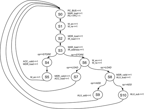
We can implement this using a basic VHDL architecture that implements each state using a new state type and a case statement to manage the flow of the state machine. The basic VHDL architecture follows and it includes the basic synchronous machine control section (reset and clock) and the management of the next stage logic.
You can see from this VHDL that the first process (state_sequence) manages the transition of the current_state to the next_state and also the reset condition. Notice that this is a synchronous machine and as such waits for the rising_edge of the clock, and that the reset is asynchronous. The second process (state_machine) waits for a change in the state or the opcode and this is used to manage the transition to the next state, although the actual transition itself is managed by the state_sequence process. This process is given in the VHDL here:
8.3.7 Summary of a Simple Microprocessor Implemented in VHDL
Now that the important elements of the processor have been defined, it is a simple matter to instantiate them in a basic VHDL netlist and create a microprocessor using these building blocks. It is also a simple matter to modify the functionality of the processor by changing the address/data bus widths or extend the instruction set.
8.4 A Simple Embedded Processor Implemented in Verilog
As in the case of the VHDL model we can implement common functions in a series of Verilog files for use in the key blocks of the processor. The architecture has been implemented in a slightly different manner, to illustrate a different approach. In both cases an internal bus has been used, which is analogous to the approach taken in early processors; however, a more direct approach can also be taken where the internal registers are accessed directly.
8.4.1 The Program Counter
The program counter (PC) needs to have the system clock and reset connections, and the system bus (defined as inout so as to be readable and writable by the PC register block). In addition, there are several control signals required for correct operation. The first is the signal to increment the PC (pc_inc), the second is the control signal to load the PC with a specified value (pc_load) and the final is the signal to make the register contents visible on the internal bus (pc_valid). This signal ensures that the value of the PC register will appear to be high impedance (Z) when the register is not required on the processor bus. The pc value output (pc_bus) is defined as a standard logic type, with direction inout to ensure the ability to read from and write to the bus.
The architecture for the program counter must handle all of the various configurations of the program counter control signals and also the communication of the data into and from the internal bus correctly. The PC model has an asynchronous part and a synchronous section. If the pc_valid goes low at any time, the value of the pc_bus signal should be set to Z across all of its bits. Also, if the reset signal goes low, then the PC should reset to zero.
The synchronous part of the model is the increment and load functionality. When the clk rising edge occurs, then the two signals pc_load and pc_inc are used to define the function of the counter. The precedence is that if the increment function is high, then regardless of the load function, the counter will increment. If the increment function (pc_inc) is low, then the PC will load the current value on the bus, if and only if the pc_load signal is also high.
The resulting Verilog code is given below:
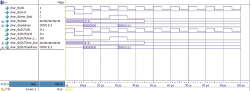
We can test this using a test bench that first resets the program counter (PC) to initialize it, increments, then loads in a set value (in this case 4), resets the counter and finally sets the valid signal to low so as to disable the output. This is shown in the following test bench Verilog:
The resulting waveform shows the behavior as predicted (Figure 8.5):

8.4.2 The Instruction Register
The Instruction Register (IR) in a simple microprocessor is a simple register with enough bits for the address and opcode combined. For example, if the address requires 8 bits, and the opcode also requires 8 bits, then the Instruction Register needs to be 16 bits wide (8 + 8). If the output from the Memory Data Register goes onto the main bus, then this can be read into the instruction register, which is 16 bits wide in this case.
The current value of the instruction register also can be read by the Memory Address Register (MAR) or the Program Counter (PC) and so the stored value needs to be of type inout, so that it can be made valid onto the internal system bus.
The instruction register (IR) therefore has clock and reset signals, and also the same interface to the internal processor bus (ir_bus) defined as a standard logic of direction inout. The IR also has two further control signals, the first being the command to load the instruction register (ir_load), and the second being to make the required address available on the system bus (ir_valid). This consists of the opcode and address, which can be used by the controller or Program Counter.
The code for the Instruction Register is therefore given in the following listing:
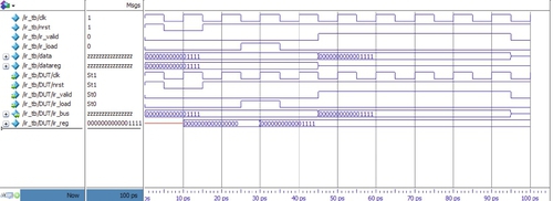
We can test this by loading in a sample instruction, and then setting it valid so that it is then seen on the bus. The test bench to achieve this is shown here:
The resulting waveform shows the behavior as predicted (Figure 8.6):
8.4.3 Memory Data Register
The memory data register is used to handle the data transferred to and from the memory unit, and this can be handled either using a bus approach (which we have used in this architecture) or separate data input and output declaration for the memory. In this case we will use a separate input and output setting for the memory; therefore, the MDR becomes a simple register which sets its output to the value of the memory output when its control signal mdr_load is high. The Memory Data Register (MDR) in a simple microprocessor needs enough bits for the address and opcode combined. For example, if the address requires 8 bits, and the opcode also requires 8 bits, then the size of the register needs to be 16 bits wide (8 + 8). If the output from the Memory Data Register goes onto the main bus, then this can be read into the instruction register, which is also 16 bits wide in this case.
The Memory Data Register (MDR) therefore has clock and reset signals, and also the same interface to the internal processor bus (mdr_bus) defined as a standard logic of direction inout. The MDR also has a further control signal, to make the required data available on the system bus (mdr_valid). This consists of the opcode and address, which can be used by the controller, Accumulator or Instruction register.
The code for the Memory Data Register (MDR) is therefore given in the following listing:
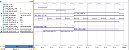
We can test this by loading in a sample instruction, and then setting it valid so that it is seen on the bus. The test bench to achieve this is shown here:
The resulting waveform shows the behavior as predicted (Figure 8.7):
8.4.4 Memory Address Register
The memory address register is used to handle the address transferred to the memory unit, and this can be handled either using a bus approach (which we have used in this architecture) or direct input declaration for the memory. In this case we will use a bus setting for the memory, therefore the MAR becomes a simple register which sets its output to the value of the required address from the IR or PC when its control signal mar_load is high. The Memory Address Register (MAR) in a simple microprocessor needs enough bits for the address. For example, if the address requires 8 bits then the The size of the register needs to be 8 bits wide.
The Memory Address Register (MAR) therefore has clock and reset signals, and also the same interface to the internal processor bus (mar_bus) defined as a standard logic of direction inout, however only the first 8 bits are used.
The code for the Memory Address Register (MAR) is therefore given in the listing below
We can test this by loading in a sample instruction, and then setting it valid so that it is seen on the bus. The test bench to achieve this is shown below:
The resulting waveform shows the behavior as predicted (Figure 8.8):
8.4.5 The Arithmetic and Logic Unit
The Arithmetic and Logic Unit (ALU) has the same clock and reset signals as the PC, and also the same interface to the bus (alu_bus) defined as a type inout. The ALU also has three further control signals, which can be decoded to map to the 8 individual functions required of the ALU. The ALU also contains the Accumulator (ACC) which is an input of the size defined for the system bus width. There is also a single bit output alu_zero which goes high when all the bits in the accumulator are zero.
The function of the ALU is to decode the alu_op in binary form and then carry out the relevant function on the data on the bus, and the current data in the accumulator. If the alu_valid is low, the the bus value should be set to Z for all bits. If the reset signal (nest) is low, then the register value internally should be set to all 0. On the rising edge of the clock, the value on the bus shall be sent to the internal register and the command shall be decoded. The resulting Verilog model is given as follows:
We can test this by loading in a sample instruction, and then setting it valid so that it is then seen on the bus. The test bench to achieve this is shown here, and in this case after initializing the accumulator to all zeros, the hex value 0012 is loaded, with the binary equivalent 0000 0000 0001 0010, which is seen in Figure 8.9.
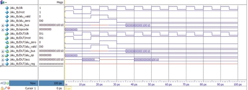
The resulting waveform shows the behavior as predicted:
8.4.6 The Memory
The processor requires a RAM memory, with an address register (MAR) and a data register (MDR). There therefore needs to be a load signal for each of these registers: mdr_load and mar_load. As it is a memory, there also needs to be an enable signal (m_en), and also a signal to denote Read or Write modes (m_rw). Finally, the connection to the system bus is a standard inout vector as has been defined for the other registers in the microprocessor.
As there is a full description of a sample memory in Chapter 11, Memory, the code is not repeated at this point.
8.4.7 Microcontroller Controller
The operation of the processor is controlled in detail by the sequencer, or controller block. The function of this part of the processor is to take the current program counter address, look up the relevant instruction from memory, move the data around as required, setting up all the relevant control signals at the right time, with the right values. As a result, the controller must have the clock and reset signals (as for the other blocks in the design), a connection to the global bus, and finally all the relevant control signals must be output.
Using this entity, the control signals for each separate block are then defined, and these can be used to carry out the functionality requested by the program. The architecture for the controller is then defined as a basic state machine to drive the correct signals. The basic state machine for the processor is defined in Figure 8.4 shown previously in this chapter.
The outline Verilog Controller is shown below; however, there are so many states it has been cut down to illustrate the architecture of the model.
8.4.8 Summary of a Simple Verilog Microprocessor
Now that the important elements of the processor have been defined, it is a simple matter to instantiate them in a complete Verilog model and create a microprocessor using these building blocks. It is also a simple matter to modify the functionality of the processor by changing the address/data bus widths or extend the instruction set.
8.5 Soft Core Processors on an FPGA
While the previous example of a simple microprocessor is useful as a design exercise and helpful to gain understanding about how microprocessors operate, in practice most FPGA vendors provide standard processor cores as part of an embedded development kit that includes compilers and other libraries. For example, this could be the MicroBlazeTM core from Xilinx or the NiosTM core supplied by Altera. In all these cases the basic idea is the same: that a standard configurable core can be instantiated in the design and code compiled using a standard compiler and downloaded to the processor core in question.
Each soft core is different and rather than describe the details of a particular case, in this section the general principles will be covered and the reader is encouraged to experiment with the offerings from the FPGA vendors to see which suits their application the best.
In any soft core development system there are several key functions that are required to make the process easy to implement. The first is the system building function. This enables a core to be designed into a hardware system that includes memory modules, control functions, DMA functions, data interfaces, and interrupts. The second is the choice of processor types to implement. A basic Nios II or similar embedded core will typically have a performance in the region of 100-200MIPS, and the processor design tools will allow the size of the core to be traded off with the hardware resources available and the performance required.
8.6 Summary
The topic of embedded processors on FPGAs would be suitable for a complete book in itself. In this chapter the basic techniques have been described for implementing a simple processor directly on the FPGA and the approach for implementing soft cores on FPGAs have been introduced.