Design Automation of FPGAs
Abstract
With the increasing complexity and size of digital designs targeted at FPGAs, the days of hand designing the logic code for hardware at the lowest level (i.e., able to be downloaded directly to the device) have long gone. Designers now must rely on design automation tools to manage the code, syntax checking, simulation and synthesis functions. In this chapter we will introduce some of the key concepts and highlight how they can be used most effectively.
5.1 Introduction
With the increasing complexity and size of digital designs targeted at FPGAs, the days of hand designing the logic code for hardware at the lowest level (i.e., able to be downloaded directly to the device) have long gone. Designers now must rely on design automation tools to manage the code, syntax checking, simulation, and synthesis functions. In this chapter we will introduce some of the key concepts and highlight how they can be used most effectively.
5.2 Simulation
5.2.1 Simulators
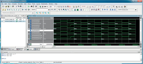
Simulators are a key aspect of the design of FPGAs. They are how we understand the behavior of our designs, check the results are correct, identify syntax errors and even check postsynthesis functionality to ensure that the designs will operate as designed when deployed in a real device. There are a number of simulators available (all the main design automation vendors provide software) and the FPGA vendors also will supply a simulator usually wrapped up with the design flow software for their own devices. This altruistic approach is very useful in learning to use FPGAs as, while they are clearly going to be targeted with libraries at the vendor’s devices, the basic simulators tend to be fully featured enough to be very useful for most circumstances. One of the most prevalent simulators is the ModelSim® from Mentor Graphics, which is generally wrapped in with the Altera and Xilinx design software kits and is very commonly used in universities for teaching purposes. It is a general-purpose simulator which can cater for VHDL, Verilog, SystemVerilog and a mixture of all these languages in a general simulation framework. A screen shot of ModelSim in use is shown in Figure 5.1 and it shows the compilation window and a waveform viewer. There are other ways to use the tool including a transcript window and variable lists rather than waveforms—useful in seeing transitions or events.
5.2.2 Test Benches
The overall goal of any hardware design is to ensure that the design meets the requirements of the design specification. In order to measure and determine whether this is indeed the case, we need not only to simulate the design representation in a hardware description language (such as VHDL or Verilog), but also to ensure that whatever tests we undertake are appropriate and demonstrate that the specification has been met.
The way that designers can test their designs in a simulator is by creating a test bench. This is directly analogous to a real experimental test bench in the sense that stimuli are defined and the responses of the circuit measured to ensure that they meet the specification.
In practice, the test bench is simply a model that generates the required stimuli and checks the responses. This can be in such a way that the designer can view the waveforms and manually check them, or by using appropriate HDL constructs to check the design responses automatically.
5.2.3 Test Bench Goals
The goals of any test bench are twofold. The first is primarily to ensure that correct operation is achieved. This is essentially a functional test. The second goal is to ensure that a synthesized design still meets the specification (particularly with a view to timing errors).
5.2.4 Simple Test Bench: Instantiating Components
Consider a simple model of a VHDL counter given as follows:
This simple model is a simple counter with a clock and reset signal, and to test the operation of the component we need to do several things.
First, we must include the component in a new design. So we need to create a basic test bench. The listing below shows how a basic entity (with no connections) is created, and then the architecture contains both the component declaration and the signals to test the design.
This test bench will compile in a simulator, and needs to have definitions of the input stimuli (clk and rst) that will exercise the circuit under test (CUT).
If we wish to add stimuli to our test bench we have some significant advantages over our model; the most appealing is that we generally do not need to adhere to any design rules or even make the code synthesizable. Test bench code is generally designed to be off chip and therefore we can make the code as abstract or behavioral as we like and it will still be fit for purpose. We can use wait statements, file read and write, assertions and other nonsynthesizable code options.
5.2.5 Adding Stimuli
In order to add a basic set of stimuli to our test bench, we could simply define the values of the input signals clk and rst with a simple signal assignment:
Clearly this is not a very complex or dynamic test bench, so to add a sequence of events we can modify the signal assignments to include numerous value, time pairs defining a sequence of values.
In our simple example, we wish to go from a reset state to actively counting and so after the rst signal has been initialized to 0, and then set to 1, the clk signal will then increment the counter. In our example we have used a process to set up the clock repetition and a separate process to initialize and then remove the reset.
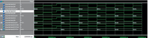
While this method is useful for small circuits, clearly for more complex realistic designs it is of limited value. Another approach is to define a constant array of values that allow a number of tests to be carried out with a relatively simple test bench and applying a different set of stimuli and responses in turn. The resulting behavior can then be analyzed looking at the waveforms with measurements and markers to ensure the correct timing and functionality, as is shown in Figure 5.2.
For example, we can exhaustively test our simple two-input logic design using a set of data in a record. A record is simply a collection of types grouped together defined as a new type. With a new composite type, such as a record, we can then create an array, just as in any standard type. This requires another type declaration, of the array type itself. With these two new types we can simply declare a constant (of type data_array) that is an array of record values (of type testdata) that fully describe the data set to be used to test the design. Notice that the type data_array does not have a default range, but that this is defined by the declaration in this particular test bench. The beauty of this approach is that we can change from a system that requires every test stimulus to be defined explicitly, to one where a generic test data process will read values from predefined arrays of data. In the simple test example presented here, an example process to apply each set of test data in turn could be implemented as follows:
There are several interesting aspects to this piece of test bench VHDL. The first is that we can use behavioral VHDL (wait for 100 ns) as we are not constrained to synthesize this to hardware. Secondly, by using the range operator, the test bench becomes unconstrained by the size of the data set. Finally, the individual record elements are accessed using the hierarchical construct test_data(i).in0 or test_data(i).in1 respectively.
5.2.6 Assertions
Assertions are a method of mechanically testing values of variables under strict conditions and are prevalent in automated tests of circuits. This is a method by which the timing and values of variables (i.e., signals) can be evaluated against test criteria in a test bench and thus the process of model validation can be automated. This is particularly useful for large designs and also to ensure that any changes do not violate the overall design. It is important to note that assertions are not used in many senses to debug a model, but rather to check it is correct in a more formal sense.
For example, we can set an internal variable (flag) to highlight a certain condition (for example, that two outputs have been set to ‘1’), and then use this with an assert statement to report this to the designer and when it has occurred. For example, consider this simple VHDL code:
If the condition occurs, then during a simulation the assertion will take place and the message reported in the transcript:
This is very useful from a verification perspective as the user can see exactly when the error occurred, but it is a bit cumbersome for debug purposes. The severity of the assertion can be one of note, warning, error, and failure.
The same basic mechanism operates in Verilog, with the same keyword assert being used. If we consider the same example, the Verilog code would be something like this:
In Verilog, the severity command resulting from the assertion can be $fatal, $error (which is the default severity) and $warning.
5.3 Libraries
5.3.1 Introduction
A typical HDL such as Verilog or VHDL as a language on its own is actually very limited in the breadth of the data types and primitive models available. As a result, libraries are required to facilitate design reuse and standard data types for model exchange, reuse, and synthesis. The primary library for standard VHDL design is the IEEE library. Within the IEEE Design Automation Standards Committee (DASC), various committees have developed libraries, packages, and extensions to standard VHDL. Some of these are listed below:
• IEEE Std 1076 Standard VHDL Language
• IEEE Std 1076.1 Standard VHDL Analog and Mixed-Signal Extensions (VHDL-AMS)
• IEEE Std 1076.1.1 Standard VHDL Analog and Mixed-Signal Extensions - Packages for Multiple Energy Domain Support
• IEEE Std 1076.4 Standard VITAL ASIC (Application Specific Integrated Circuit) Modeling Specification (VITAL)
• IEEE Std 1076.6 Standard for VHDL Register Transfer Level (RTL) Synthesis (SIWG)
• IEEE Std 1076.2 IEEE Standard VHDL Mathematical Packages (math)
• IEEE Std 1076.3 Standard VHDL Synthesis Packages (vhdlsynth)
• IEEE Std 1164 Standard Multivalue Logic System for VHDL Model Interoperability (Std_logic_1164)
Each of these working groups consists of volunteers who come from a combination of academia, EDA industry and user communities, and collaborate to produce the IEEE Standards (usually revised every 4 years).
5.3.2 Using Libraries
In order to use a library, first the library must be declared: library ieee; for each library. Within each library a number of VHDL packages are defined, which allow specific data types or functions to be employed in the design. For example, in digital systems design, we require logic data types, and these are not defined in the basic VHDL standard (1076). Standard VHDL defines integer, Boolean, and bit types, but not a standard logic definition. This is obviously required for digital design and an appropriate IEEE standard was developed for this purpose, IEEE 1164. It is important to note that IEEE Std 1164 is NOT a subset of VHDL (IEEE 1076), but is defined for hardware description languages in general.
5.3.3 Std_logic Libraries
In order to use a particular element of a package in a design, the user is required to declare their use of a package using the USE command. For example, to use the standard IEEE logic library, the user needs to add a declaration after the library declaration as follows:
The std_logic_1164 package is particularly important for most digital designs, especially for FPGA, because it defines the standard logic types used by ALL the commercially available simulation and synthesis software tools and is included as a standard library. It incorporates not only the definition of the standard logic types, but also conversion functions (to and from the standard logic types) and also manages the conversion between signed, unsigned, and logic array variables.
5.4 std_logic Type Definition
As it is such an important type, the std_logic type is described in this section. The type has the following definition:
| U | uninitialized. This signal hasn’t been set yet. |
| X | unknown. Impossible to determine this value/result. |
| 0 | logic 0 |
| 1 | logic 1 |
| Z | High Impedance |
| W | Weak signal, can’t tell if it should be 0 or 1 |
| L | Weak signal that should probably go to 0 |
| H | Weak signal that should probably go to 1 |
| - | Don’t care |
These definitions allow resolution of logic signals in digital designs in a standard manner that is predictable and repeatable across software tools and platforms. The operations that can be carried out on the basic std_logic data types are the standard built-in VHDL logic functions:
• nand
• or
• nor
• xor
• xnor
• not
An example of the use of the std_logic library would be to define a simple logic gate, in this case a three input nand gate as shown in the following listing. The logic pin types are now defined using the IEEE standard library type std_logic rather than the default bit type.
5.5 Synthesis
5.5.1 Design Flow for Synthesis
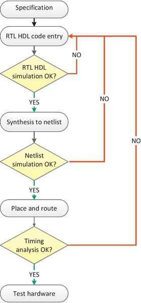
The basic HDL design flow is shown in Figure 5.3 and, as can be seen from this figure, synthesis is the key stage between high level design and the physical place and route which is the final product of the design flow. There are several different types of synthesis ranging from behavioral, to RTL and finally physical synthesis.
Behavioral synthesis is the mechanism by which high-level abstract models are synthesized to an intermediate model that is physically realizable. Behavioral models that are not directly synthesizable can be written in VHDL and so care must be taken with high-level models to ensure that this can take place, in fact. There are limited tools that can synthesize behavioral VHDL and these include the Behavioral Compiler from Synopsys, Inc. and MOODS, a research synthesis platform from the University of Southampton.
RTL (Register Transfer Level) synthesis is what most designers call synthesis, and is the mechanism whereby a direct translation of structural and register level VHDL can be synthesized to individual gates targeted at a specific FPGA platform. At this stage, detailed timing analysis can be carried out and an estimate of power consumption obtained. There are numerous commercial synthesis software packages, including Design Compiler®, and Synplify®, but this is not an exhaustive list as there are numerous offerings available at a variety of prices.
Physical synthesis is the last stage in a synthesis design flow and is where the individual gates are placed (using a floor plan) and routed on the specific FPGA platform.
5.5.2 Synthesis Issues
Synthesis basically transforms program-like VHDL into a true hardware design (netlist). It requires a set of inputs, a VHDL description, timing constraints (when outputs need to be ready, when inputs will be ready, data to estimate wire delay), a technology to map to (list of available blocks and their size/timing information) and information about design priorities (area vs. speed). For big designs, the VHDL will typically be broken into modules and then synthesized separately. 10K gates per module was a reasonable size in the 1990s; however, tools can handle a lot more now.
5.6 RTL Design Flow
Register Transfer Level (RTL) VHDL is the input to most standard synthesis software tools. The VHDL must be written in a form that contains registers, state machines (FSM), and combinational logic functions. The synthesis software translates these blocks and functions into gates and library cells from the FPGA library. The RTL design flow is shown in Figure 5.3. Using RTL VHDL restricts the scope of the designer as it precludes algorithmic design, as we shall see later. This approach forces the designer to think at quite a low level, making the resulting code sometimes verbose and cumbersome. It also forces structural decisions early in the design process, which can be restrictive and not always advisable, or helpful.
The design process starts from RTL (Register Transfer Level) VHDL, as follows:
• Simulation (RTL): needed to develop a test bench (VHDL).
• Synthesis (RTL): targeted at a standard FPGA platform.
• Timing Simulation (Structural) simulate to check timing.
• Place and Route using standard tools (e.g., Xilinx Design Manager).
Although there are a variety of software tools available for synthesis (such as LeonardoSpectrumTM or Synplify), they all have generally similar approaches and design flows.
5.7 Physical Design Flow
Synthesis generates a netlist of devices plus interconnections. The Place and Route software figures out where the devices go and how to connect them. The results are not as good as you’d perhaps like: a 40-60% utilization of devices and wires is typical. The designer can trade off run time against greater utilization to some degree, but there are serious limits. Typically the FPGA vendor will provide a software toolkit (such as the Xilinx Design Navigator, or Altera’s Quartus® II tools) that manages the steps involved in physical design. Regardless of the particular physical synthesis flow chosen, the steps required to translate the VHDL or EDIF output from an RTL Synthesis software program into a physically downloadable bit file are essentially the same and are listed here:
2. Map
3. Place
4. Route
5. Generate accurate timing models and reports
6. Create binary files for download to device
5.8 Place and Route
There are two main techniques to place and route in current commercial software: which are recursive cut and simulated annealing.
5.8.1 Recursive Cut
In a recursive cut algorithm, we divide the netlist into two halves, and move devices between halves to minimize the number of wires that cross cut (while keeping the number of devices in each half the same). This is repeated to get smaller and smaller blocks.
5.8.2 Simulated Annealing
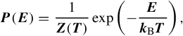
The simulated annealing method Laarhoven [9] uses a mathematical analogy of the cooling of liquids into solid form to provide an optimal solution for complex problems. The method operates on the principle that annealed solids will find the lowest energy point at thermal equilibrium and this is analogous to the optimal solution in a mathematical problem. The equation for the energy probability used is defined by the Boltzmann distribution given by Equation (5.1):
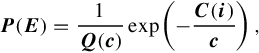
where Z (T) is the partition function, which is a normalization factor dependent on the temperature T, kB is the Boltzmann constant, and E is the energy. This equation is modified into a more general form, as given by (5.2), for use in the simulated annealing algorithm.
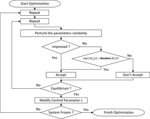
where Q(c) is a general normalization constant, with a control parameter c, which is analogous to temperature in Equation (5.1). C(i) is the cost function used, which is analogous to the energy in Equation (5.1). The parameters to be optimized are perturbed randomly, within a distribution, and the model tested for improvement. This is repeated with the control parameter decreased to provide a more stable solution. Once the solution approaches equilibrium, then the algorithm can cease. A flowchart of the full algorithm applied is given in Figure 5.4.
5.9 Timing Analysis
Static timing analysis is the most commonly used approach. In static timing analysis, we calculate the delay from each input to each output of all devices. The delays are added up along each path through the circuit to get the critical path through the design and hence the fastest design speed. This works as long as there are no cycles in the circuit; however, in these cases the analysis becomes harder. Design software allows you to break cycles at registers to handle feedback if this is the case. As in any timing analysis, the designer can trade off some accuracy for run time. Digital simulation software such as ModelSim or Verilog will give fast results, but will use approximate models of timing, whereas analog simulation tools like SPICE will give more accurate numbers, but take much longer to run.
5.10 Design Pitfalls
The most common mistake that inexperienced designers make is simply making things too complex. The best approach to successful design is to keep the design elements simple, and the easiest way to manage that is efficient use of hierarchy. The second mistake that is closely related to design complexity is not testing enough. It is vital to ensure that all aspects of the design are adequately tested. This means not only carrying out basic functional testing, but also systematic testing, and checking for redundant states and potential error states. Another common pitfall is to use multiple clocks unnecessarily. Multiple clocks can create timing-related bugs that are transient or hardware dependent. They can also occur in hardware and yet be missed by simulation.
5.10.1 Initialization
Any default values of signals and variables are ignored. This means that you must ensure that synchronous (or asynchronous) sets and resets must be used on all flip-flops to ensure a stable starting condition. Remember that synthesis tools are basically stupid and follow a basic set of rules that may not always result in the hardware that you expect.
5.10.2 Floating Point Numbers and Operations
Data types using floating point are currently not supported by synthesis software tools. They generally require 32 bits and the requisite hardware is just too large for most FPGA and ASIC platforms.
5.11 Summary
This chapter has introduced the practical aspect of developing test benches and validating VHDL models using simulation. This is an often overlooked skill in VHDL (or any hardware description language) and is vital to ensuring correct behavior of the final implemented design. We have also introduced the concept of design synthesis and highlighted the problem of not only ensuring that a design simulates correctly, but also how we can make sure that the design will synthesize to the target technology and still operate correctly with practical delays and parasitics. Finally, we have raised some of the practical implementation issues and potential problems that can occur with real designs, and these will be discussed in more detail in Part 4 of this book.
An important concept useful to define here is the difference between validation and verification. The terms are often confused, leading to problems in the final design and meeting a specification. Validation is the task of ensuring that the design is doing the right thing. If the specification asks for a low pass filter, then we must implement a low pass filter to have a valid design. We can even be more specific and state that the design must perform within a constraint. Verification, on the other hand, is much more specific and can be stated as doing the right thing right. In other words, verification is ensuring that not only does our design do what is required functionally, but in addition it must meet ALL the criteria defined by the specification, preferably with some headroom to ensure that the design will operate to the specification under all possible operating conditions.
Finally, we have introduced several design tools and it should be stressed that this in no way indicates a preference, and of course there are a large number of design tools available including some open source tools (many more than I have listed in this chapter). As is usual with the world of design automation, it is really a matter of user preference as to which tools are used.