
SI3N4/SiO2 Planar Photonic Structures Fabricated by Focused Ion Beam
Device Research Laboratory, Applied Physics Dept. Gleb Wataghin, Univ. of Campinas–UNICAMP, 13083-970 Campinas, SP, Brazil
Center for Semiconductor Components, University of Campinas–UNICAMP, 13083-870 Campinas, SP, Brazil
1. Introduction
Micro-optical resonators are essential components in optical integrated systems, as they facilitate the selective capture, release, and storage of photons as well as interaction with matter and other photons. As an example, microdisks1 and micro-rings2,3 are elements that provide extremely long photon lifetimes that can be used for spectral filtering and for highly efficient nonlinear photon interactions.4,5 The small volumes and the high photonic lifetime in micro-resonators are very important, for example, to enable four-wave mixing (FWM) with a single pumping frequency.6
However, coupling light to and from the micro-resonator is still achieved via hybrid integration, typically using tapered silica fibers.7 In this chapter, we present a new technique for the fabrication of structures with monolithically integrated resonators and planar tapered waveguides, all based on SiNx/SiO2 layers deposited on silicon.
We use an approach that combines nanofabrication techniques based on focused ion beam (FIB) milling and smoothing8 and conventional microfabrication techniques. We have fabricated resonators coupled to tapered waveguides using this approach. Tapered waveguides with 0.8 dB/cm losses were obtained. Finally, we observed the photon generation at a micro-ring resonance due to FWM generated by pumping at a subsequent micro-ring resonance.
2. Fabrication and characterization
All structures were fabricated on a silicon (100) substrate. First, a 0.5 μm SiO2 layer is obtained by wet oxidation.9 Subsequently, we deposited 0.3 μm of silicon nitride (Si3N4) over the SiO2 layer using an electron cyclotron resonance (ECR) plasma deposition (process parameters: 125 sccm of SiH4, 20 sccm of Ar and 2.5 sccm of N2 at 3 mtorr process pressure with 250 W of rf power for 40 min).
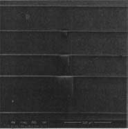
Figure 1. SEM micrograph of Si3N4 structures fabricated by conventional micro-fabrication techniques. The square mesas will be used for the fabrication of resonators.
Fabrication of tapered waveguides coupled to the resonators was accomplished using a hybrid technique involving conventional fabrication and FIB milling. The first step consisted of fabricating Si3N4 ridges connected to square mesas. The ridges were 10 μm wide, whereas the mesas ranged from 25 to 200 μm on the side. Figure 1 shows an SEM micrograph of the fabricated structures. The Si3N4 was etched chemically in a buffered oxide etchant for 8 minutes.
The second step of the fabrication involved FIB milling of the squares to form resonators and of the waveguide structures near the squares to form adiabatic tapering for field delocalization. The FIB was performed using a dual-beam FIB/SEM 200 model from FEI, with gallium as the ion source. The inset in Fig. 2(a) shows the programmed milling pattern. The milling is done with an emission current of 50 pA and a voltage of 30 kV. The low current provides high resolution (20 nm) for the process. Figure 2(a) shows a SEM micrograph of a microdisk resonator (50 μm radius) coupled to a tapered waveguide (0.5 μm wide). The tapered 0.2 μm wide waist is aligned with the resonator center. The taper length is 300 μm. The time to complete the milling was 45 min. Figure 2(b) shows a micro-ring resonator obtained with the milling of the internal region of the microdisk described above. The ring has 0.5 μm width and the gap between the resonator and the guide is 0.2 μm.
The last step of the fabrication consisted of a 2 μm SiO2 layer deposition over the entire structure. This step was done using the ECR system with 200 seem of SiH4, 20sccm of O2, and 20 sccm of Ar at 10 mtorr; 750 W of rf power for 10 min. The structures are then cleaved orthogonally to the waveguide direction.
The expected guiding and coupling behavior of the structures can be predicted by using a 2D finite element method (FEM) of the Comsol Multiphysics™ package. Figure 3(a) shows a schematic drawing of the Si3N4 waveguide structure used in the simulation, whereas Fig. 3(b) shows the simulated transverse electric (TE) modes. The waveguide is multimode, as expected. Figure 3(c) shows the light confinement in the tapered region of the waveguide. The wide evanescence field allows coupling to structures as far as 1 μm from the waist. Obviously, a narrower tapered region gives a higher evanescence field, as shown in Fig. 3(d) for a 0.2 μm waist. Still, in order to best match the phase velocity between the waveguide and the ring we fabricated both structures with the same width of 0.5 μm.
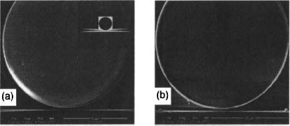
Figure 2. (a) SEM micrograph of a 50 μm radius microdisk 0.2 μm distant from the 0.5 μιτι wide tapered waveguide waist (inset shows the ion milling pattern); (b) SEM micrograph of a 0.5 μm width micro-ring (50 μιn radius) fabricated on the same disk.
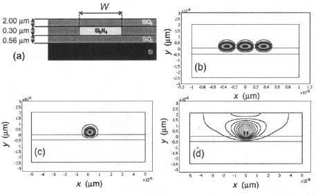
Figure 3. (a) Schematic drawing of the Si3N4 waveguide structure; (b–d) electric field contours for the TE mode for waveguides with width W = 10 μm (b), 0.5 μm (c), and 0.2 μm (d).
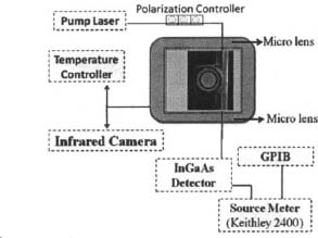
Figure 4. Experimental set-up.
Figure 4 shows the experimental set-up used for the optical characterization of our structures. The sample was positioned over a block with a length smaller than the waveguide length (about 1 mm). This block was set over a Peltier element for temperature control. A multi-channel tunable laser (1500 to 1600 nm) and a polarization controller were used as the light source. A GRIN rod lens for collimation and a micro lens for focus were used to couple light to and from the planar structures and the fiber. The signal output was sent to an InGaAs detector.
Before measuring our resonators, we fabricated a 2500 μm long waveguide with a 300 μm long tapered region of 0.2 μm width to evaluate the transmission losses. Figure 5 shows the spectrum of this waveguide. Fabry-Perot oscillations with a free spectral range (FSR) of 0.28 nm are observed. Losses of 0.6 cm–1 are obtained using the Hakki-Paoli method,10 assuming a reflectivity of 12% at the facets based on the Fresnel coefficient. This corresponds to 0.8 dB/cm loss.
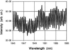
Figure 5. Spectrum of a 2500 μm long and 10 μm wide waveguide with a 300 μm tapered region and a waist of 0.2 μm. The associated FRS is 0.28 nm.
Transmission measurements for the waveguide coupled to resonator structures were subsequently performed on a 2100 μm long waveguide coupled to a 25 μm radius micro-ring with the dimensions described above. The solid line in Fig. 6(a) shows the transmission spectrum. We observe two transmission minima at 1551.0 nm and 1558.6 nm.The dotted line shows the simulated transmission spectrum. The dashed line shows the simulated electromagnetic field intensity inside the micro-ring resonator. The experimentally observed minima match the expected micro-ring resonances. As expected, the transmission minima occur at the micro-ring maxima, in good agreement with the simulation. Figure 6(b) shows the Fourier transform of the transmission spectrum. There are two maxima: one at 0.3 nm related to the FSR of the Fabry-Perot cavity and another at 7.6 nm related with the FSR of the micro-ring resonator coupled to the tapered waveguide. This result is in agreement with simulations of the 25 μm radius disk.
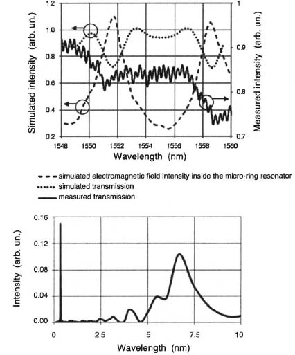
Figure 6. Transmission spectrum of a micro-ring resonator with 25 μm radius and 0.5 μm width coupled to a tapered waveguide of 0.5 μm waist at a distance of 0.2 μm (top); Fourier transform of the spectrum (bottom).
In order to study photon creation within the resonator, we chose one of the resonances for pumping the micro-ring resonator and repeated the transmission experiment. Figure 7 shows the transmission spectrum (dotted line) obtained previously and a new spectrum for a 1558.6 nm pump signal with constant power of 2 dBm and a varying probe signal from 1545 to 1560 nm with constant power of 6 dBm (solid line). The enhanced transmission at 1551 nm is a result of the generation of extra photons at this resonance wavelength. The generation of extra photons at this resonance is most probably due to the pumping at the subsequent micro-ring mode at 1558.6 nm. This is possible since four-wave mixing between neighboring modes in micro-ring resonators is allowed for materials with small chromatic dispersion. In these cases, both the angular momentum and the photon energy vary linearly with the azimuthal quantum number.5,11
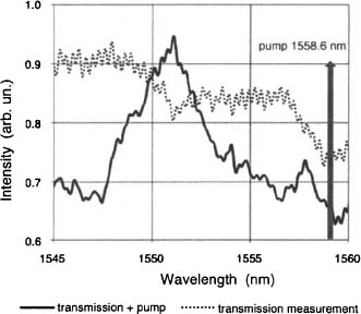
Figure 7. Transmission spectra: dotted line shows the transmission without pumping; solid line shows the transmission with 2 dBm pumping at the 1558.6 nm resonance.
5. Conclusions
We have presented a new technique for the fabrication of Si3N4/SiO2 planar resonators coupled to tapered waveguides. This new technique consists of conventional microfabrication combined with high-resolution focused ion beam processing. Tapered waveguides with typical loss of 0.8 dB/cm were obtained. Also, we observed photon generation at a micro-ring resonance due to four-wave mixing generated by pumping at a subsequent micro-ring resonance.
Acknowledgments
The authors would like to acknowledge the Conselho Nacional de Desenvolvimento Científico e Tecnológico (CNPQ), the Fundaçâo de Amparo à Pesquisa do Estado de São Paulo (FAPESP), the Centro de Pesquisa em Óptica e Fotônica (CEPOF) and Institutos Nacionais de Ciência e Tecnología (INCT) with Fotônica para Comunicações Ópticas (FOTONICOM), for the financial support. The authors would like to thank José Godoy Filho for assistance in the oxidation process.
References
1. P. Ε. Barclay, K. Srinivasan, O. Painter, B. Lev, and H. Mabuchi, “Integration of fiber-coupled high-Q SiNx microdisks with atom chips,” Appl. Phys. Lett. 89, 131108(2006).
2. T. Barwicz, M. Popovic, P. Rakich, M. Watts, H. Haus, Ε. Ippen, and H. Smith, “Micro-ring-resonator-based add-drop filters in SiN: fabrication and analysis,” Opt. Express 12, 1437 (2004).
3. S. Zheng, H. Chen, and A. Poon, “Micro-ring-resonator cross-connect filters in silicon nitride: Rib waveguide dimensions dependence,” IEEE J. Select. Topics Quantum Electronics 12, 1380 (2006).
4. K. J. Vahala. “Optical microcavities,” Nature 424, 839 (2003).
5. P. Del’Haye, A. Schliesser, O. Arcizet, T. Wilken, R. Holzwarth, and T. J. Kippenberg, “Optical frequency comb generation from a monolithic microresonator,” Nature 450, 1214 (2007).
6. K. Inoue, “Four-wave mixing in an optical fiber in the zero-dispersion wavelength region,”J. Lightwave Technol. 10, 1553 (1992).
7. S. M. Spillane, T. J. Kippenberg, O. J. Painter, and K. J. Vahala, “Ideality in a fiber-taper-coupled microresonator system for application to cavity quantum electrodynamics,” Phys. Rev. Lett. 91, 043902 (2003).
8. F. Vallini, D. S. L. Figueira, P. F. Jarschel, L. A. M. Barea, A. A. G. Von Zuben, and N. C Frateschi, “Effects of Ga+ milling on InGaAsP quantum well laser with mirrors milled by focused ion beam”, J. Vac. Sci. Technol. B 27, L25 (2009).
9. K. K. Lee, D. R. Lim, L. C. Kimerling, J. Shin, and F. Cerrina, “Fabrication of ultralow-loss Si/SiO2 waveguides by roughness reduction,” Optics Lett. 26, 1888(2001).
10. B. W. Hakki and T. L. Paoli, “Gain spectra in GaAs double-heterostructure injection lasers,” J. Appl. Phys. 46, 1299 (1975).
11. M. K. Chin and S. T. Ho, “Design and modeling of waveguide-coupled single-mode micro-ring resonators,” J. Lightwave Technol. 16, 1433 (1998).