
Graphene-Based Terahertz Devices: Concepts and Characteristics
CNEL, University of Aizu, Aizu-Wakamatsu 965-8580, Japan
RIEC, Tohoku University, Sendai 980-8577, Japan
Dept. of Electrical Engineering, SUNY-Buffalo, Buffalo 14260, U.S.A.
Institute of Semiconductor Physics NAS, Kiev 03028, Ukraine
Institute for Physics of Microstructures RAS, Nizhny Novgorod 603950, Russia
Dept. of ECSE, Rensselaer Polytechnic Institute, Troy 12180, U.S.A.
1. Introduction
Graphene, i.e. a monolayer of carbon atoms densely packed in a two-dimensional honeycomb structure, graphene bilayers, and patterned graphene structures have captured the great interest of researchers and device engineers. Modification of a laterally uniform graphene layer (GL) into an array of nanostrips, which are usually referred to as graphene nanoribbons, results in the transformation of two-dimensional (2D) linear electron and hole gapless energy spectra into sets of one-dimensional (1D) subbands accompanied by the appearance of an energy gap. Graphene bilayers also exhibit the gapless energy spectra, but with the dispersion relations close to parabolic ones. In a transverse electric field, the energy gap opens and the electron and hole dispersion relations are modified.
Due to the features of the electron and hole energy spectra, particularly their massless, neutrino-like form, as well as of the scattering processes, GLs exhibit unique transport properties that open up wide prospects for their applications in future electronics.1-3 The features of graphene include the following:
• linear dispersion relation for electrons and holes with zero energy gap;
• strong anisotropic interband tunneling and high velocities (vw ≈ 108 cm/s) of electrons and holes, providing their ballistic transport in devices with micrometer sizes;
• formation of electrically-induced p and n regions as well as pin junctions;
• bandgap engineering possibilities due to lateral quantization in nanoribbons and transverse electric field-induced energy gaps in bilayers;
• high electron and hole mobilities (up to μ = 2 x 105 cm2/V·s at room temperatures and up to μ ~ 107 cm2/V·s at Τ < 55 K);
• exceptional mechanical properties.
These features open up prospects to create high-speed electron devices, in particular, diodes and transistors, and nano-electromechanical devices surpassing those made of the customary semiconductor materials. Owing to the gapless energy spectrum of electrons and holes in GLs and narrow bandgaps in graphene nanoribbons and graphene bilayers, graphene-based structures appears to be also very promising for various terahertz (THz) devices. In this chapter, we review and analyze several proposals of following devices:
• GL lasers with optical pumping and cascade emission of optical phonons; and
• GL injection lasers and tunneling transit-time devices with electrically induced lateral pin junctions.
2. Lasers with optically pumped GLs
A laser structure with one or several optically pumped GLs serving as the active media placed inside a Fabry-Perot resonator is shown in Figs. 1(a) and (b). The proposed optical pumping scheme4 (see also Refs. 5–7) corresponds to that shown in Fig. 1(c). The graphene structure with the two GLs can be fabricated using a Si substrate covered by a 3C-SiC film (on both sides) and subjected to annealing.8 It assumes that the electrons and holes generated by optical radiation with the photon energy ħΩ emit a cascade of optical phonons and are accumulated in the energy range E < ħΩ/2 – Nmaxħω0. Here ħω0 =200 meV is the GL optical phonon energy and Nmax is the integer of the ratio ħΩ/2ħω0, that is, the maximum number of the optical phonons in the cascade. The accumulation of the photogenerated electrons near the bottom of the conduction band and holes near the top of the valence band produces electron and hole distribution functions fe(E) =fh,(E) > 1/2 over a certain range of energies. The result is population inversion and, consequently, the negative absorption coefficient of low-energy photons. To overcome the losses associated with absorption in the substrate, mirrors, and so on, as well as to enhance the pumping efficiency, structures with multiple GLs appear to be attractive. Recently, perfect multiple GL structures (with the number of GLs up to 100) were fabricated using annealing of SiC substrates.9 A sketch of the laser with such a multiple-GL structure is shown in Fig. 2(a). However, these multiple-GL structures as the active media exhibit the following two features. First, due to the absorption of optical pumping radiation in multiple GLs, the attenuation of this radiation, and consequently, marked difference in the population and the values of the quasi-Fermi energies ΕF(k) of different GLs occurs (1 < k < K is the index and K is the total number of GLs). Second, there is a buffer bottom GL between the SiC substrate and perfect GLs. The density of electrons in the bottom GL is rather high and the electron Fermi energy ΕFB in this GL is large. This can lead to undesirable absorption of THz photons. The electron population in bottom GL and other GLs is schematically shown in Fig. 2(b). An alternative multiple-GL structure without the bottom GL can be fabricated using chemical/mechanical reactions and transferred substrate techniques (chemically etching the substrate and the highly conducting bottom GL or mechanically peeling the upper GLs and transferring them onto a Si or equivalent transparent substrate).
To obtain the lasing condition one needs to find the GL absorption coefficient as a function of the photon frequency. This coefficient is proportional to the real
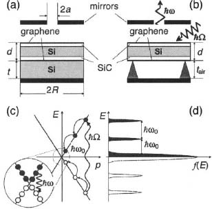
Figure 1. Schematic view of a laser based on a double-GL structure with a Si separation layer (a) and an air separation layer (b), together with the laser pumping scheme (c) and electron and hole distribution functions (d). The jagged arrows in (b) denote the directions of optical pumping radiation and output THz radiation with the photon energies ħΩ and ħω, respectively. Arrows in (c) correspond to the pertinent transitions.

Figure 2. (a) Schematic view of a laser with a multi-graphene-layer (MGL structure; (b) occupied and vacant states in different GLs under optical pumping. Arrows show transitions related to interband emission and intraband absorption of THz photons with energy ħω (interband optical pumping transitions and intraband relaxation processes of photogenerated electrons and holes are not shown).
part of the dynamic conductivity. By generalizing previously-derived formulae (see, for instance, Ref. 4) to the nonequilibrium electron-hole distributions in the structures under consideration, one obtains the following results for the real part of the dynamic conductivity in the bottom GL (if any) and other GLs, respectively:

and

Here τΒ and τ are the electron and hole momentum relaxation times in the bottom and other GLs, respectively, Τ is the electron and hole temperature, and ħ and kB are the Planck and Boltzmann constants. The quasi-Fermi energy in the kth GL EF(k) with k ≥ 1 is mainly determined by the electron (hole) density in this GL, and therefore, by the rate of photogeneration GΩ(K) by the optical radiation incident and reflected from the mirror. Using Eq. (2) for ħω = ħΩ >2EF(k), we obtain
where IΩ(k) is power density of the optical radiation at the kth GL and β = πe2/ħc ≈ 0.023. Considering the attenuation of the optical pumping radiation due to its absorption in each GL, one obtains
Here IΩ is the intensity of incident optical radiation and βB = (4πc/c)Re{σΩB}.
To achieve lasing in the multiple-GL structures under consideration, the following condition should be satisfied:

Here, EB and E(k) are the amplitudes of the THz electric field E = E(z) at the pertinent GL, whereas E1 and E2 are the amplitudes of the THz electric field near the bottom and top mirrors, respectively,
![]()
αS and ns are the absorption coefficient of THz radiation in the substrate (Si or SiC) and real part of its refractive index, r1 and r2 are the reflection coefficients of THz radiation from the mirrors, and a/R is the ration of the diameters of the output hole a and the mirror R. The THz electric field is assumed to be in the GL plane (in the xy plane). In deriving inequality (5), we neglected the finiteness of the multiple-GL thickness (in comparison with t and the THz wavelength) and disregarded the diffraction losses and reflection of THz radiation from the bottom GL.
The spatial distribution of the THz electric field can be found using the following equation:
where κω(z) is the permittivity at the THz frequency ω. The spatial dependence of κω(z) reflects a difference in its values in different layers of the resonator (in the air layer, substrate, GL structure, and in the depth of the metal mirrors). The boundary conditions for Eq. (6) correspond to the continuity of E and dE/dz, together with E and dE/dz → 0 when z → ± ∞.
In the case of double-GL structure (no bottom GL and K = 2, see Figs. 1(a) and (b)) with a relatively thick separation layer, one can put Re{σωΒ} = 0 and, as follows from Eq. (4) due to a smallness of β, GΩ(1) = GΩ(2) = IΩβ/ħΩ. For the double-GL structure in question, Eq. (5) can be reduced to the following:

Taking into account that EF(1) = EF(2) = EFT, the net dynamic conductivity becomes

The first term in the right-hand side of Eq. (8) is associated with the intraband absorption of THz radiation in the GL, whereas the second one is associated with the interband absorption and emission. When the latter is negative, that is when the interband emission prevails the interband absorption, the quantities Re {σω(1)} and Re{σω(2)} exhibit minima as a function of ω. Under sufficiently strong optical pumping when EFT is large enough, Re{σω(1)} and Re{σω (2)} can be negative in a certain range of ω. For example, Eq. (8) at Τ = 77 K, EFT =17 meV, τ = 1 ps, and ω/2π = 1.08 THz yields σω(1) = σω(2) = –5×107 cm/s. Fig. 3 shows the spatial distribution of the THz electric field and the real part of refractive index for such a laser calculated using Eq. (6) considering real values of κω(z) in different parts of the device. The pertinent quantities Q are shown in the upper right corners of the panels. Here the thicknesses of the Si layers are chosen to be t = 61 μm and d = 39 μm to maximize the THz electric field modulus just at both GL planes: E(1) = E(2) = Emax – see Fig. 3.
At r1 = r2 = 0.99, (a/R) = 0.1, αS = 0.7 cm-1, nS = 3.42 (for the Si separation layer and the substrate10), Eq. (7) provides the maximum value of Q = 2.16, which corresponds to the lasing condition. On the other hand, if t and d are not chosen properly, Q can be smaller and even fall below unity.
In the case of the MGL structure, its net thickness is small in comparison with the wavelength of THz radiation (even for K > 100), so that the amplitude of the THz electric field is approximately the same in all GLs. When the thickness of the substrate t is chosen to provide the maximum value Emax at the GLs, Eq. (5) can be rewritten as:
where
is the real part of the net dynamic conductivity of all GLs.
For concreteness, we assume that EF (k) ∞ [GΩ(k)]γ, where γ is a phenomenological parameter. This leads to
where EFT= EF(K) is the quasi-Fermi energy in the topmost GL.

Figure 3. Spatial distributions of THz electric field (solid lines) and real part of refractive index (dashed lines): (a), (b), and (d) correspond to t + d = 100 μm, (c) t + d = 110 μm.

Figure 4. Frequency dependence of the real part of dynamic conductivity Re{σω} normalized by quantity e2/4ħ for MGL structures with different number of GLs K at EFT = 30 and 50 meV. The inset on upper panel shows how the GL population varies with the GL index k, whereas the inset on lower panel demonstrates the dependences over a wider range of frequencies.
Figure 4 shows the frequency dependence of the real part of the net conductivity Re{σω} normalized by e2/4ħ calculated for MGL structures with different numbers of GLs (K = 20, 50, and 100) at different optical pumping intensities (different values of the quasi-Fermi energies in the topmost GL, EFT = 30 and 50 meV). As it seen from Fig. 4, an increase in the number of GLs leads to markedly larger absolute value of Re{σω} in the frequency range where it is negative. Fig. 5 demonstrates the spatial distribution of the THz electric field inside the Fabry-Perot resonator calculated using Eq. (6) for a laser based on an MGL structure operating at ω/2π = 1.5 THz. The thicknesses of the SiC substrate were chosen as t = 45 μm and t = 80 μm to provide maximum amplitudes of the THz field at the MGL structure. It was assumed that EFB = 400 meV, T = 300 Κ, τ = 10 ps, τB = 1 ps, and γ = 0.25. As follows from the calculations utilizing Eq. (11), the quantity EF(1) is about 0.97 EFT, 0.87 EFT, and 0.68 EFT at K = 20, 50, and 100, respectively. One can see that Re{σω} becomes negative at ω/2π > 1 THz and its absolute value is fairly large. Indeed, if K = 20-100, EFT = 30 meV, and ω/2π = 1.5 THz, one obtains Re{σω} = –(3+10)×l08 cm/s. Assuming, that r1 = r2 = 0.99, (a/R) = 0.1, αS = 2–4 cm–1, and setting for SiC substrate11 nS = 3 and t = 45 μm, one obtains Q = 3.1–13.4 ![]() 1. However, in MGL structures will less perfect GL, i.e. with shorter momentum relaxation times τ and τΒ, the minimum of Re{σω} is shifted toward higher frequencies and markedly smaller in absolute value.
1. However, in MGL structures will less perfect GL, i.e. with shorter momentum relaxation times τ and τΒ, the minimum of Re{σω} is shifted toward higher frequencies and markedly smaller in absolute value.

Figure 5. Spatial distribution of the THz electric field (solid line) and real part of refractive index (dashed line) in a laser based on a multiple-GL structure shown in Fig. 2(a) with r = 45 μm (upper panel) and t = 80 μm (lower panel) at ω/2π = 1.5 THz.
Despite stronger intraband absorption characterized by relatively small τ and τΒ, the Q > 1 condition can be satisfied in the multiple-GL structures as well, albeit several THz. The GL structures without the bottom GL can provide THz lasing at more liberal conditions.
As follows from the results obtained above, when the quasi-Fermi energy EFT in the topmost GL is about 30–50 meV, the conditions for THz lasing at the lower end of the THz range can be satisfied in multiple-GL structures even at the room temperature, particularly if the momentum relaxation times τ and τΒ are sufficiently long. At Τ = 300 K, EFT > 30 meV corresponds to the electron and hole densities σn = σp = 2 x 1011 cm–2 (markedly exceeding the thermal value, which is about 8 x 1010 cm–2). This density can be routinely experimentally achieved in optically pumped GLs. At higher temperatures, the emission of optical phonons can be envisioned as the mechanism of the electron-hole recombination12 (near the threshold of lasing and not far beyond this threshold). Experimental reports12–14 have cited densities σn = σp = 2 x 1011 cm–2, achieved at a photogeneration rate G > 1022 cm–2S –1. If ħΩ = 120–920 meV, the above photogeneration rate corresponds to the optical power density IΩ > 8–64 kW/cm2. Since lowering the temperature leads to a dramatic drop in the rate of the optical-phonon-assisted recombination, the threshold of optical pumping can be decreased by orders of magnitude at lower T < 100 K and be limited by the radiative recombination stimulated by the thermal photons.6
3. GL injection laser and tunneling transit-time devices
In gated GL structures, applied gate voltages of different polarities can result in the formation of electron and hole regions in the GLs. In particular, lateral pn or pin junctions can be electrically induced in GL with split gates.15 A device structure based on a single-GL with a lateral pin junction is shown in Fig. 6(a). When a lateral pin junction is forward biased, the electron injection into the i and p sections and the hole injection into the i and n sections can lead to population inversion, resulting in a pin-based THz injection laser.16 We can use Eq. (2) with k = 1 to calculate the dynamic conductivity for this case. However, the quasi-Fermi energy should be calculated accounting for the carrier injection and the leakage to the source and drain contacts. The electrically induced pin junctions can also be realized in the devices like that shown in Fig. 6(a), but with a multiple-GL structure. In this case, the number of effective GLs in which the p and n sections are electrically induced is limited due to the screening of the transverse electric field (associated with the gate voltages) by the preceding GLs.
The structure with the electrically induced pin junction shown in Fig. 6(a) but at reverse bias can also be used in GL tunneling transit-time (G-TUNNETT) devices.17 The G-TUNNETT structure under consideration and its band diagram (at an applied source-drain voltage V such that the lateral pin junction is reverse biased) are schematically shown in Figs. 6(a) and (b), respectively. The operation of the G-TUNNETT in question is associated with the tunneling injection in an electrically induced reverse-biased lateral pin junction and the electron and hole transit-time effects in its depleted section.

Figure 6. Schematic view of a gated GL structure with electrically induced pin junction (a) and the band diagram when the pin junction is reverse-biased (b).

Figure 7. Frequency dependences of real part of the ac conductance calculated for uniform (upper panel) and strongly nonuniform (lower panel) electric-field spatial distributions in the i section for different lengths of i section: solid lines correspond to 2l = 0.5 μm (τ = 0.25 ps) and dashed lines correspond to 2l = 0.7 μm (τ = 0.35 ps). Insets magnify the real and imaginary parts of the ac conductance vs. its real part with ωτ as a parameter for different lengths of i section (right panel).
It is assumed that apart from a dc component of the source drain-voltage V0 > 0, the net source-drain voltage V also contains an ac component δVexp(–iωt), where δV and ω are the signal amplitude and frequency, respectively.
The probability of interband tunneling in graphene is a fairly sharp function of the angle between the direction of the electron (hole) motion and the x-direction (from the source to the drain). Taking this into account, we disregard the spread in the x-component of the velocity of the injected electrons and assume that all the generated electrons and holes propagate in the x-direction with the velocity υx = υw. Using the formula for the interband tunneling probability,15 we take into account that the rate of the local tunneling generation G ∞ E312, where E = E(x) is the electric field in the I. As a result, for the signal component of the tunneling rate one can obtain δGω = (3G0/2)(δVωV0), where G0 = G0(x) is the dc tunneling rate. Calculating the induced ac terminal (source-drain) current created by the electrons and holes generated in the i section and propagating with the velocity υx = υw using the Shockley-Ramo theorem, one obtains the following formulae for the ac conductance δωSD = δJωSD/δVω:
Here σ0 = J0/V0 is the dc conductance, J0 is the dc current, c = 2C/3σ0τ, C is the lateral pin junction capacitance, ![]() ο(ξ) is the Bessel function, and τ = l/υW is the characteristic transit time of electrons and holes across the i section of length 21. Expressions (12) and (13) correspond to the cases of uniform and strongly nonuniform tunneling generation of the electron-hole pairs, respectively. In the former case, the electric field is constant, E = V/2l. In the latter case, it is assumed that the electric field is concentrated near the edges of the quasi-neutral p and n sections.
ο(ξ) is the Bessel function, and τ = l/υW is the characteristic transit time of electrons and holes across the i section of length 21. Expressions (12) and (13) correspond to the cases of uniform and strongly nonuniform tunneling generation of the electron-hole pairs, respectively. In the former case, the electric field is constant, E = V/2l. In the latter case, it is assumed that the electric field is concentrated near the edges of the quasi-neutral p and n sections.
Figure 7 shows the real parts of the ac conductance σωSD as functions of the signal frequency f = ω/2π calculated for G-TUNNETTs with both uniform and strongly nonuniform electric-field distributions for different lengths of the i section. The phase diagrams, that is the pertinent Ιm{σωSD} vs. Re{σωSD} dependences for the device with a uniform electric-field distribution are also shown in Fig. 7. The real part exhibits a pronounced oscillatory behavior with frequency, including changes in sign. The frequency dependence of the imaginary part corresponds to the dominance of the inductive component at low frequencies (associated with the contribution of electrons and holes) and the capacitive component at high frequencies (due to the contribution of the geometrical capacitance). The relative values of the real part of the ac conductance at the first minima at 2l = 0.5 μm is as follows: Re{σωSD}σ0 = –0.034 (at f1 = 1.75 THz) and Re{σωSD}/σ0 = –0.141 (at f1 = 1.25 THz) for the uniform and nonuniform distributions, respectively. At V0 = 0.1-1 V, for the above data one obtains Re{σωSD} = –(0.71–2.26)×1011 s–1 and Re{σωSD} = –(2.94–9.37)×l011 s–1. The largest of these values, corresponding to several tens of mS/mm, markedly exceed those in some new concept THz devices based on different materials. The above estimates and Fig. 7 show that the real part of the ac conductance can be negative at the frequencies f > 1 THz in the G-TUNNETT structures with the i section length only moderately smaller than one micron. The G-TUNNETT can be used in THz oscillators with a complementary resonant cavity. Apart from the G-TUNNETTs with a single pin junction, structures with multiple cascaded pin junctions (see Fig. 8) exhibiting higher injection efficiency and better coupling with the electromagnetic radiation can be utilized. In the device structures based on the electrically induced pin junctions, such as injection lasers and G-TUNNETTs, the highly conducting split gates can serve as the waveguides.

Figure 8. Schematic view of a cascaded G-TUNNETT structure and band diagram.
4. Conclusions
We have considered new THz device concepts based on GLs, utilizing the specific features of the energy spectrum of graphene, namely, the zero energy gap and the constant velocity of electrons and holes. We demonstrated that novel THz sources can generate the electromagnetic radiation with the frequencies starting from about 1 THz at room temperatures.
Apart from the devices considered above, GLs can be used in THz photodetectors (see, for instance, Ref. 18). The controlled opening of the energy gap in graphene nanoribbons and graphene bilayers opens up prospects of high-performance THz transistors19,20 and tunable phototransistors for THz radiation.21,22
References
1. C. Berger, Ζ. Song, T. Li, et al., “Ultrathin epitaxial graphite: 2D electron gas properties and a route toward graphene-based nanoelectronics,” J. Phys. Chem. 108, 19912 (2004).
2. K. S. Novoselov, A. K. Geim, S. V. Morozov, et al., “Two-dimensional gas of massless Dirac fermions in graphene,” Nature 438, 197 (2005).
3. A. H. Castro Neto, F. Guinea, Ν. M. R. Peres, K. S. Novoselov, and A. K. Geim, “The electronic properties of graphene,” Rev. Mod. Phys. 81, 109 (2009).
4. V. Ryzhii, M. Ryzhii, and T. Otsuji, “Negative dynamic conductivity of graphene with optical pumping,” J. Appl. Phys. 101, 083114 (2007).
5. F. Rana, “Graphene terahertz oscillators,” IEEE Trans. Nanotechnol. 7, 91 (2008).
6. A. Satou, F. T. Vasko, and V. Ryzhii, “Nonequilibrium carriers in intrinsic graphene under interband photoexcitation,” Phys. Rev. B 78, 115431 (2008).
7. A. A. Dubinov, V. Ya. Aleshkin, M. Ryzhii, T. Otsuji, and V. Ryzhii, “Terahertz laser with optically pumped graphene layers and Fabry-Perot resonator,” Appl. Phys. Express 2, 092301 (2009).
8. Yu. Miyamoto, H. Handa, E. Saito, et al, “Raman-scattering spectroscopy of epitaxial graphene formed on SiC film on Si substrate,” e-J. Surf. Sci. Nanotech. 7, 107(2009).
9. P. Neugebauer, M. Orlita, C. Faugeras, A.-L. Barra, and M. Potemski, “How perfect can graphene be?” Phys. Rev. Lett. 103, 136403 (2009).
10. E. D. Palik, Handbook of Optical Constants of Solids, New York: Academic Press, 1998, p. 192.
11. J. H. Strait, P. A. George, J. M. Dawlaty, S. Shivaraman, M. Chandrashekhar, F. Rana, and M. G. Spencer, “Emission of terahertz radiation from SiC,” Appl. Phys. Lett. 95, 051912 (2009).
12. F. Rana, P. A. George, J. H. Strait, J. Dawlaty, S. Shivaraman, M. Chandrashekhar, and M. G. Spencer, “Carrier recombination and generation rates for intravalley and intervalley phonon scattering in graphene,” Phys. Rev. B 79, 115447(2009).
13. D. Sun, Z.-K. Wu, C. Divin, et al., “Ultrafast relaxation of excited Dirac fermions in epitaxial graphene using optical differential transmission spectroscopy,” Phys. Rev. Lett. 101, 157402 (2008).
14. J. M. Dawlaty, S. Shivaraman, M. Chandrashekhar, F. Rana, and M. G. Spencer, “Measurement of ultrafast carrier dynamics in epitaxial graphene,” Appl. Phys. Lett. 92, 042116 (2008).
15. V. V. Cheianov and V. I. Fal’ko, “Selective transmission of Dirac electro ns and ballistic magnetoresistance of n-p junctions in graphene,” Phys. Rev. B 74, 041403 (2006).
16. M. Ryzhii and V. Ryzhii, “Injection and population inversion in electrically induced p-n junction in graphene with split gates,” Japan. J. Appl. Phys. 46, L 151 (2007).
17. V. Ryzhii, M. Ryzhii, V. Mitin, and M. S. Shur, “Graphene tunneling transit-time terahertz oscillator based on electrically induced p-i-n junction,” Appl. Phys. Express 2, 034503 (2009).
18. F. T. Vasko and V. Ryzhii, “Photoconductivity of intrinsic graphene,” Phys. Rev. B 77, 195433(2008).
19. M. Ryzhii, A. Satou, V. Ryzhii, and T. Otsuji, “High-frequency properties of a graphene nanoribbon field-effect transistor,” J. Appl. Phys. 104, 114505 (2008).
20. V. Ryzhii, M. Ryzhii, A. Satou, T. Otsuji, and N. Kirova, “Device model for graphene bilayer field-effect transistor,” J. Appl. Phys. 105, 104510 (2009).
21. V. Ryzhii, V. Mitin, M. Ryzhii, N. Ryabova, and T. Otsuji, “Device model for graphene nanoribbon phototransistor,” Appl. Phys. Express 1, 06302 (2008).
22. V. Ryzhii and M. Ryzhii, “Graphene bilayer field-effect phototransistor for terahertz and infrared detection,” Phys. Rev. B 79, 245311 (2009).