
Treating the Case of Incurable Hysteresis in VO2
Dept. of Physics and Astronomy, SUNY-Stony Brook, NY 11794 and NY State Center for Advanced Sensor Technology, Stony Brook, NY 11794, U.S.A.
Dept. of Electrical and Computer Engineering, SUNY-Stony Brook and NY State Center for Advanced Sensor Technology, Stony Brook, NY 11794, U.S.A.
NY State Center for Advanced Sensor Technology, Stony Brook, NY 11794, U.S.A.
1. Introduction
Phase transitions present an opportunity for a useful application utilizing a natural proximity of two phases with different physical properties and an ability to trigger the transition by varying a transition-controlling parameter, such as temperature, or magnetic field, etc. There exist applications based on magnetic transitions, optical transitions, metal-insulator transitions, and superconducting transitions. Some of these phase transitions, especially those classified as first-order transitions (i.e. accompanied by the release or absorption of latent heat), are hysteretic in nature, so that the two phases transform into each other along different routes depending on the direction of change of a transition-controlling parameter. Such hysteresis can be essential for an application. A well-known example (in this case, of a hysteretic second-order transition) is a ferromagnetic material that can be magnetized by an external magnetic field and, because of the hysteresis, will remain magnetized when the external field is reduced to zero. This is used for making permanent magnets and in magnetic storage of information. The stored, “memorized” magnetization can be erased, which requires specific steps to be taken, such as going around the magnetic hysteresis loop with diminishing external fields. In other cases, however, the utilization of a phase transition is hindered by its hysteresis. The “memory” of the previous history that is beneficial in magnetic materials may become detrimental in other applications, where the irreversible (or, more precisely, not easily reversible) change in a given material’s property, e.g. resistivity, may be undesirable.
In this chapter we consider VO2, a material undergoing a first-order phase transition, and target an application – infrared (IR) visualization utilizing resistive bolometers made of VO2 – in which hysteresis causes problems. We offer a way of operation that circumvents these problems. The applied aspects of IR visualization vis-à-vis our proposed approach are discussed in our recent publication,1 and we will refer to it in a number of instances for further details and references. Here we want to explain the essence of the method and touch upon its physics fundamentals.
2. Hysteretic semiconductor-metal phase transition in VO2 - major and minor loops
The resistivity of VO2 changes by 3–5 orders of magnitude in a spectacular semiconductor-to-metal phase transition around 68 °C.2 In addition to resistivity, other properties change in this first-order phase transition, including crystalline structure and optical constants. In single crystals, the transition is very sharp, with hysteresis width of 0.5-2 °C,3 whereas in polycrystalline films it is broader, with hysteresis width (as measured in the middle of a transition) of 10-20 °C. The resistive transition measured in one of our VO2 films can be seen in Figs. 1-4 (look at the outside major loop; ignore for now the inner or minor loops or their parts which are shown on these figures). The films used in these measurements were prepared on Si/SiO2 substrates by pulsed laser deposition; details of sample preparation and measurements can be found in Ref. 1. On the log(R) vs. T plot starting from room temperature, the resistivity first follows the semiconducting S-phase slope with increasing Τ and then falls sharply along the right (heating) branch of the transition reaching metallic M-phase. When the temperature is decreased, the resistivity follows the left (cooling) branch, forming a closed loop between two transition-end points TS and TM. As can be seen in Figs. 1-4, the resistivity below the transition, in the S-phase, is about 3 orders of magnitude higher than in the M-phase above the transition. The hysteresis width in the middle of this log(R) vs. T plot is about 15 °C, while the total width of a hysteretic region is TM – TS ~ 50 oC.

Figure 1. Major hysteresis loop of VO2 film with a number of minor loops initiated from various temperatures T0 on (a) the cooling branch (CB), T0 → T0+ΔΤ → T0 with ΔT = 25 °C, and (b) the heating branch (HB), T0 → T0–ΔΤ → TQ with ΔΤ= 45 °C.
For a variety of reasons, despite the many proposals to use this transition in applications, almost none materialized. One commercial and military application in which the use of VO2 was initially envisioned is IR visualization (night vision) based on resistive microbolometers. However, technology eventually settled on a “poor cousin” of VO2, a non-transitioning mixed VOx oxide, mainly to avoid hysteresis, which greatly complicates bolometer operation, as was mentioned in the introduction and will be discussed in more detail below.
The major hysteretic loop encompasses all the points on the (T, R) plane that can serve as starting points of minor hysteretic loops. In particular, minor loops can be initiated at any point along the outer lines of the major loop. In Fig. 1, we show several minor loops which were traced by reversing the temperature change at various points along the major loop: in Fig. 1(a), minor loops are starting from points along the cooling branch (CB); in Fig. 1(b), from points along the heating branch (HB). The loops shown in Fig. 1 cover wide temperature ranges of 25 °C in Fig. 1(a) and 45 °C in Fig. 1(b). A number of minor loops traced over a narrower temperature range of 10 °C are shown in Fig. 2.

Figure 2. Minor loops with ΔT = 10 °C, the inset shows the way in which temperature was changed in this measurement.
3. How hysteresis causes problems in bolometric readout – forward and backward excursions
A bolometer reacts to a temperature change ΔT by changing its resistance by ΔR. The larger the ΔR for a given ΔT, the greater is the sensitivity. At the same time, very large resistance R is detrimental because of bolometric sensor Joule heating during readout, the difficulty of matching to the electronic readout circuit, and higher noise, both Johnson and 1/f.1 Thus, a commonly-used measure of the bolometric material’s sensitivity is the logarithmic derivative (1/R)(ΔR/ΔT) known as the temperature coefficient of resistance, or TCR. In other words, it is not the high ΔR, but high ΔR/R that is desired.
The steep semiconductor to metal transition seems to promise great sensitivity (high TCR), comparable to the sensitivity that can be achieved in a transition-edge superconducting sensor, which provided the original incentive to employ such a transition in VO2.4 Why then was it not used? The main reason is the hysteresis.
Let us look in more detail on how hysteresis causes problems. To be specific, let us consider a bolometer positioned at a working point (T0, R0) on a steep heating branch (HB), kept there using a temperature controller as T0 is above room temperature. Then, an influx of energy (this could be an IR signal) momentarily heats it up, increasing its temperature by ΔT and decreasing its resistance by a large ΔR, as shown in Fig. 3

Figure 3. Forward excursions originating from point (T0, R0) on an HB and from point (T0’, R0’) on a CB, tracing open curves ending at (T0, R) on an HB and at (T0’, R0’) on a CB. The backward excursions from (70, R0) and (T0’, R0’) return to the points of their origin following closed minor loops. Note that this figure is not a schematic drawing; it shows measured loops and parts of loops.
Once the heat input has been removed (which happens in resistive bolometers used in IR visualization at least 30 times per second), the bolometer returns back to the temperature T0; however, because of the hysteresis, the (T, R) path on the way back differs from the path in the forward direction: the resistance will not come back to R0, but instead will move along the part of the minor loop to a point (T0, R) as indicated in Fig. 3. If a bolometer now experiences a subsequent second heat pulse, the result will be very different. This cannot be tolerated in a bolometric sensor subject to a train of pulses. In order to avoid this problem the bolometer should be reset after each pulse, which can only be done by going all the way out of the hysteresis loop, reaching temperatures either below TS or above TM, as can be seen in Fig. 1. While such resetting can be done, it requires large temperature excursions (we will call a round-trip temperature change T0 → T0±ΔT → T0 an excursion) followed each time by temperature stabilization at the working point T0. With bolometers receiving signals at 30–60 Hz (video rates), this is not practical. The problem with the different return path we just outlined has been described in the literature,5 and the readout problems caused by hysteresis were acknowledged6 as the major contributing factor in killing the original proposal4 of using high TCR found in a VO2 transition.
A word about terminology: as was said, we call a round trip T0 → T0±ΔT → T0 an excursion. We will take the excursion length ΔT to be a positive quantity, and show the plus or minus sign in front of it explicitly. If temperature of the initial part of an excursion changes in the same direction as the major loop progression, we call it a forward excursion; if it starts in the opposite direction, it is a backward excursion. Thus, in Fig. 3 on the HB, the excursion from (T0, R0) to (T0, R) is a forward one; the other one, forming a closed loop, is a backward one. We could discuss similar processes originating from point (T0’, R0’) on a CB (they are also shown in Fig. 3), keeping in mind that on a CB decreasing temperature corresponds to the forward direction, and increasing temperature to the backward direction.
Because of the hysteresis, forward and backward excursions produce dramatically different results. While a forward excursion T0 → T0+ΔT → T0 on a HB traces an open curve from (T0, R0) to (T0, R), a backward excursion T0 → T0-ΔT → T0 produces a closed minor loop, which has a much smaller slope near (T0, R0. The slope increases with the excursion ΔT, thereby introducing a nonlinearity in log(R) vs. T – the TCR now depends on the value of ΔT. Similar processes take place on a CB, see Fig. 3.
To summarize, hysteresis causes the following two distinct types of problems:
• forward excursions produce open (T, R) curves, a “memory effect” that is unacceptable in a bolometer taking multiple repeated measurements;
• backward excursions produce closed loops, so that bolometer re-setting is not required. However, the double-valued nature of such a minor loop makes readout ambiguous, and variable TCR found in minor loops is unacceptable, or at least detrimental, producing nonlinearities in the bolometric response, with larger ΔT corresponding to larger TCR.
4. Nonhysteretic branches in resistivity
Now let us examine Fig. 2 in more detail. We see that most of the minor loops in Fig. 2 are hysteretic, but we also notice that some of them are rather flat and nearly single-valued, particularly those near the major loop ends TS and TM. In studying minor loops with progressively smaller excursions ΔT we discovered that for sufficiently small ΔT minor loops flatten out, degenerating into what we call nonhysteretic branches (NHBs). Although some minor loops become flat with ΔT = 10 °C (Fig. 2), all of them become flat at or below ΔT ΝΗΒ = 4–5 °C, as can be seen in Fig. 4.
An NHB can be initiated from any point on the major loop, either on a HB or on a CB; NHBs are linear in log(R) vs. Τ with negative slopes (semiconducting TCRs). Two representative NHBs measured in round-trip excursions are plotted in Fig. 5.
The NHBs are single valued to the precision of our measurements, except for the temperature intervals near the attachment point T0 and the turning point T0 ± ΔT, where they sometimes appear double-valued, exhibiting a small loop and a fork, as seen in Fig. 5(a). These features depend on the rate of temperature sweep; they are probably instrumental effects resulting from a lag between film surface and thermometer temperatures.1

Figure 4. Minor loops with ΔT= 5 °C; inset shows the temperature variation during this measurement.
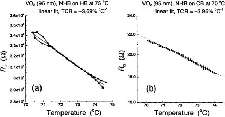
Figure 5. (a) NHB attached to the HB, with R□= 31 kΩ; TCR = –3.69 % °C”1; (b) NHB attached to the CB, with R□ = 20 Ω; despite this low R, TCR = -3.96 % °C-1.
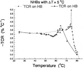
Figure 6. Absolute values of TCR vs. T0 for various NHBs around the major loop.
The TCRs of various NHBs from Fig. 4 are plotted vs. T0 in Fig. 6 for both HB and CB. The S-phase TCR at 25 °C is 3.3 % °C-1, which is considerably higher than a typical TCR ≈ 2 % °C-1 at 25 °C found in the literature on VOx.1,6 In an intrinsic semiconductor, the bandgap EG is given by1 2(|TCR|)kBT2. Substituting |TCR| = 0.033 and Τ = 25 °C = 298 K, we obtain EG = 0.51 eV, in fair agreement with the bandgap value in VO2 single crystals.3
As we see in Fig. 6, NHBs logarithmic slopes peak at 65 °C on the CB and 75 °C on the HB, with maximum values of 4% °C-1 and 6% °C-1 decreasing sharply above the peaks. We note that the highest TCRs on the sides of the major loop are found at these same temperatures.
5. Theoretical model
We will present a theoretical model that provides a qualitative explanation of the observed behavior and has predictive power that will be put to a test in the next Section.
The hysteretic region in VO2 is a mixed state consisting of both the S-phase and M-phase regions, or domains. Each such region located in a film around a point with spatial coordinates (x, y) transitions into the other phase at its own temperature TC, with the variation in TC arising from nonuniformities of composition, variations in the local strain, etc. In a macroscopic sample TC(x, y) is quasi-continuously distributed. We assume that the local transition within a domain is sharp; further, we assume that a uniform isolated domain would transition without a hysteresis. In this we differ from much of the VO2 hysteresis literature7 in which it is usually assumed that each domain, in addition to a local TC, has its own coercive temperature and a rectangular hysteresis loop. We note that single crystals have very small hysteresis;3 it seems natural to extrapolate this to the case of an ideally uniform microscopic (or nanoscopic) region that would have zero hysteresis. In our picture hysteresis is the result of interaction between different phases in a multi-domain macroscopic sample, as will be detailed below.
At a given temperature Τ inside the major hysteretic loop, some parts of the film have TC(x, y) < Τ and some TC(x, y) > T. In the first approximation, the boundary wall between the S and M phases is determined by the condition TC(X, y) = T. In this approximation, the wall is highly irregular and its ruggedness corresponds to the scale at which one can define the local TC(X, y), i.e. the characteristic length scale of the nanoscopic phase domains. On closer inspection, however, we need a refinement that takes into account the boundary energy of the phase domain wall itself. This boundary energy is positive and to minimize its contribution to the free energy, the domain walls are relatively smooth.
Let us examine the process of boundary motion. For concreteness, let us consider the heating branch. Below the percolation transition, the M-phase resembles lakes in the S-phase mainland. With increasing temperature, the area of the M-phase increases, so the lakes grow in size. When a boundary of a given lake is far from the other lakes, infinitesimal ±dT changes boundary length by infinitesimal amount ±dL, and the lake area by ±dAM. In other words, when the lakes are sufficiently separated, we envision a continuous, reversible, hysteresis-free process of M ↔ S area redistribution, with neighboring configurations differing microscopically, what we call area breathing.
Let us now look at the formation of a link between two neighboring regions, which is the elementary step in the topological evolution of a global percolation picture. Consider two metallic lakes that are about to merge. Since the boundary is smooth, at some Τ the distance between the lakes becomes smaller than the radius of curvature of either lake at the point they will eventually touch. Therefore, at some critical TCR the following two configurations will have equal energies: one comprising two disconnected M-phase lakes that are nearly but not quite touching, and the other with a finite link formed, Figs. 7(a) and 7(b) respectively.

Figure 7. Semiconductor-metal boundary, with the metallic phase shown as shaded. Top row (a), (b) corresponds to temperature T1 and the bottom row (c), (d) to temperature T2 >T1.
Both configurations are characterized by equal boundary lengths and therefore have equal free energy. In the thermodynamic sense one could call the TCR the critical temperature for the link formation, if we could wait long enough. The actual transition forming a local link, however, does not occur at that temperature because of an immense kinetic barrier between these two macroscopically different configurations. The transition occurs at a higher T0 = Τ + ΔT* when it is actually forced, i.e. when the two phases touch at a point. Here ΔT is the coercive temperature. As can be seen, in our picture coercive temperature arises as a result of having a boundary between different phases; it does not preexist within each domain. We associate the steep slopes of the major loop with the quasi-continuous formation of such links, i.e. with local topological changes, specifically with the merger of metallic lakes on the HB and semiconductor lakes on the CB. Near Ts and TM, the global map consists of widely separated M and S lakes, respectively. In these regions we expect to see nonhysteretic behavior; indeed, looking at Fig. 2 we see that AT= 10 °C NHBs are largely non-hysteretic within ~20 °C from TS and ~15°C from TM.
Consider now a small excursion backwards from T0 on the HB. As the temperature decreases, some of the M-phase recedes and the S-phase grows, changing the geometry of the global two-phase map. However, topologically, the last formed M-link does not disappear immediately for the same kinetic reason. One has two S regions that need to touch in order to wipe out the M-link. It takes a backward excursion of amplitude ΔT* to establish an S-link and thus disconnect the last M-link. So long as we are within ΔT, i.e. stay on the same NHB, the area of S and M domains changes continuously, but the topology is stable and no new links are formed. Within the range of that stable or frozen topology, ΔT* = ΔTNHB, the resistivity of NHB will be single-valued and its temperature dependence will be controlled by the percolating semiconductor phase. This explains why NHBs have semiconducting slopes.
We introduced here a notion of frozen topology, which describes a global two-phase map with stable connecting links between regions of the same phase, while geometrical shape of the two phases is allowed to change, or breathe. One can also envision NHBs in which this breathing stops altogether, no switching between phases taking place, keeping the geometrical outlines fixed, this being the case of frozen geometry. Clearly frozen geometry implies frozen topology, but not the other way around. We will see below that both conditions actually exist and can be observed in a transitioning VO2.
We can further address the observed phenomenon of TCR enhancement in some of the NHBs, where TCRs exceed the S-phase value – see Fig. 6. We note that for all NHBs, on both branches of the major loop, higher Τ implies increased fraction of M-phase, even if no new links are formed. This smooth change in geometry will produce additional temperature dependence adding to the semiconductor slope within a NHB, i.e. higher TCR. This effect will be stronger in the temperature intervals where this smooth change in geometry is more active, and it will cease to exist in the regions of frozen geometry, where the NHB slope will be determined only by the percolating S-phase. We will refer to this effect in explaining our optical reflectance measurements below.
Theoretical models that explain the data are good, but those that correctly predict new behavior are better. What can we predict based on our model?
We recall that hysteresis takes place in all physical properties that change in the phase transition. In addition to resistivity, optical constants, such as the refractive index n, change in the VO2 transition. In a small uniform domain, n changes abruptly at TC, from ns to nM. In a macroscopic film, there is a distribution of TC(x, y) and therefore, in a temperature range of co-existing S and M phases, TS < Τ < TM, the sample will contain some S domains with nS and some M domains with nM. As phases transform with changing T, the macroscopic film will exhibit a temperature-dependent hysteretic w(T), much like the previously discussed R(T). Indeed, optical properties exhibit hysteretic transition as a function of temperature. Among them, optical reflectivity is probably the easiest optical quantity to measure, although the details of how optical reflectivity behaves in a phase transition in a film with thickness comparable with the wavelength of light have to do not only with n(T) but also with thin-film interference. This issue is discussed in detail in Ref. 8 (and in references therein), and we will not repeat the explanation here. The result is that, when Τ increases from 25 °C to 100 °C and decreases back to 25 °C, optical reflectivity Rλ(T) at a fixed wavelength λ traces a hysteresis loop between certain values RλS and RλM, these values being determined by a number of factors, including the choice of λ, film thickness, nS and nM. We can further expect that backward excursions from the points on the major optical loop will produce optical NHBs, for the same reason they exist in R(T), and indeed we observed them, as will be seen below.
Based on our theoretical model, what specific behavior can we predict in optical reflectivity vs. T? Reflectivity is measured at wavelengths exceeding the nano-domain scale. It is largely determined by thin-film interference, with two-phase material between the film surfaces (in the Fabry-Perot resonator) having the average value of n, the latter depending on the volume fraction of S and M phases (volume fraction of nS and nM), which in a thin film becomes the area fraction of the two phases. In contrast, resistivity depends on the connectivity (links) of the percolating phase. Let AS and AM be the areas of S-phase and M-phase in a two-dimensional sample (thin film), so that the total sample area is A = AS + AM. Clearly, as A does not depend on T, dAM/dT = –dAs/dT, i.e. the area of one phase grows at the expense of the other. The optical slope dRλ/dT observed in optical NHB must be proportional to this area redistribution slope, with the maximum in dRλ/dT reflecting the maximum in dAM/dT. According to our explanation of TCR enhancement over the S-phase value, the highest TCR should be found at the point that has the highest rate of area redistribution dAM/dT = –dAS/dT, and, therefore, at the point which corresponds to the maximum optical NHB slope dRλ/dT. Likewise, zero rates of area redistribution (frozen geometry) corresponding to dRλ/dT = 0, should correspond to unenhanced S-phase TCR. In the next section we will have a chance to verify these specific predictions.
The percolation picture also helps to understand why dRλ/dT exhibits such a maximum in the first place. With changing temperature, the boundary moves, each section of the boundary line advancing in the direction normal to this line at any given temperature. It is clear that the highest rate of change of the area of each phase will therefore occur when the boundary is the longest, i.e. at the percolation transition. If our picture is correct, then the observed peak in TCR vs. T0 in Fig. 6 occurs right at the percolation transition, allowing its detection. Finally, we see in Fig. 6 that above the peak, i.e. above the percolation transition, TCRs decrease quickly. Indeed, if the M-phase percolates, it shorts out the S-phase, and such decrease is to be expected.
6. NHBs in optical reflectivity - testing the theoretical model
In order to test some of the predictions of our model, simultaneously with the resistive measurements presented in Figs. 2 and 4, we measured reflectivity Rλ(T) at a fixed wavelength λ. The optical signal was taken from the space between the voltage probes used in a four-probe resistivity measurement. In Fig. 8(a) we show major loop and minor hysteresis loops with ΔT= 10 °C in optical reflectivity Rλ(T) (i.e. this is an optical analog of Fig. 2). Some of the minor loops degenerate into optical NHBs, just like in resistivity measurements of Fig. 2. Additionally, we see that some minor loops are T-dependent, while others are not, and that T-dependent ones tend to be double-valued, while Γ-independent ones degenerate into NHBs.
In Fig. 8(b) we plot data for the same sample with shorter 5 °C excursions (i.e. this figure is an optical analog of Fig. 4). We see that all minor loops degenerated into NHBs, in complete analogy to Fig. 4, and according to our model of Section 5. Some of these NHBs, those closer to the center of the major loop, are T-dependent, while others closer to the loop limits are not. The T-dependent ones correspond to hysteretic minor loops in Fig. 8(a), while T-independent NHBs correlate with non-hysteretic behavior in Fig. 8(a).
Figure 9 combines the optical slopes dRλ/dT of NHBs from Fig. 8(b) with the TCR data from Fig. 4 for both HB and CB branches. Clearly, the predictions of our model are borne out: the peaks in dRλ/dT on both branches coincide almost precisely with the peaks in TCR, and the region in which dRλ/dT ≈ 0 corresponds to TCR ≈ (TCR)s. Further, if dRλ/dT ≈ 0 is a signature of a frozen geometry, it seems natural that, in the absence of S ↔ M transitions, minor loops should degenerate into NHBs more readily, as we observe in Fig. 8. The small (~2 degrees) misalignment of dRλ/dT and TCR peaks in Fig. 9 is due to the fact that the factors that determine the overall shape of the major optical loop, such as interference effects,8 should also to some extent affect the NHB slopes. Likewise, the relatively small deviation of the TCR in the dRλ/dT ≈ 0 region from the S-phase value – the observed shallow TCR minimum on the CB – can be ascribed to secondary causes. We do not think that these details disprove or diminish the impressive overall agreement of the main features predicted by our model.

Figure 8. (a) Major hysteresis loops in optical reflectivity with minor loops, excursion length ΔT= 10 °C (λ = 800 nm); (b) same data with ΔT= 5 °C.

Figure 9. A combined plot of TCR and dRλ/dT vs. T from various NHBs around the major loop plotted on one graph, exhibiting expected correlations.
The overall shape of the optical hysteresis and the range between pure-phase reflectivity values of RλS and RλM can be changed by making measurements at different wavelengths λ. In addition to the λ = 800 nm measurements shown in Fig. 8, we also measured Rλ(T) at λ = 503 nm. The λ = 503 nm optical loop looks entirely different than the one shown in Fig. 8. Yet the dRλ/dT exhibits the same peaks as in Fig. 9 and these peaks correlate with TCR peaks, confirming that we are indeed observing intrinsic S ↔ M area redistribution and not the effects of interference, etc.
Summing up, we proposed a qualitative theoretical picture, described in Section 5, without detailed mathematical modeling, which would be rather involved (perhaps a task for the future). We describe hysteresis in the framework of a percolation transition, as arising from interaction of S and M phases, specifically ascribing strong hysteretic effects to link formation between the two phases. This model corresponds to a number of observed features in both resistive and optical data. The most impressive agreement is achieved in the explanation of a subtle effect of TCR enhancement over the S-phase value in a range of NHBs where optical slopes correlate with TCRs, leaving no doubt that we understand the reason for TCR enhancement correctly.
8. Resistive microbolometers in NHB regime
A detailed discussion of the NHB method in the context of IR visualization with resistive microbolometers (the uncooled focal plane array or UFPA technology) is given in Ref. 1. Here we only give a brief summary. Good quality, single-phase VO2 films may replace VOx mixed oxide as sensor material in pixilated bolometric array. Despite using VO2, hysteresis is eliminated when a sensor array operates within an NHB. The NHB will be chosen on the basis of its desired resistance, which can be adjusted over a wide range in order both to match the readout circuit amplifier and to minimize noise and Joule heating. The resistance will be 2-3 orders of magnitude smaller than the unacceptably high VO2 resistance at 25 °C, while maintaining semiconducting TCR. We have seen NHBs with resistance as low as 20 Ω having TCR ≈ –4% °C-1. We can also choose an NHB to maximize TCR, which, as we have seen, varies between different NHBs around the major loop, peaking at the percolation transition at a value as high as 6% °C-1. The operating temperature TOP (i.e. the temperature at which the sensor array is stabilized awaiting the projected IR signal) will be chosen within an NHB, either near one of the ends or in the middle of the available range (total NHB width) ΔTNHB = 4–5 °C. Because of the hysteresis, the process of reaching TOP starting from room temperature requires performing specific heating and cooling steps. Specifically, positioning an array at TOP will require: on the HB, warming up to T0 and cooling down to TOP; on the CB, warming up to above TM, cooling down to T0, and again warming up to TOP. If TOP is chosen in the middle of an NHB, the last step requires cooling down from T0 to (T0 – ΔTNHB/2) on the HB or warming up from T0 to (T0 – ΔTΝΗΒ/2) on the CB.
9. Summary
We found a regime of operation within a hysteretic phase transition that avoids hysteresis within a limited range of a transition-controlling parameter. This may benefit applications utilizing a phase transition but suffering from complications introduced by hysteresis. One such application is IR visualization with resistive microbolometers. We propose to use VO2 as a sensor material, operating it in the nonhysteretic branch (NHB) regime. Partial shorting out of the S-phase by the M-phase lowers sensor resistance; the degree of admixture of M-phase determines the value of this resistance, making it adjustable. At the same time, because of the S-phase percolation, NHB has semiconducting R(T). The TCR in this case can be considerably higher than in the pure S-phase due to a smooth change of geometry (but not the topology) of S-M areas within an NHB. A similar NHB regime exists in optical reflectivity. Optical reflectivity slopes correlate with TCRs, revealing the reason for TCR enhancement in some of the NHBs over the S-phase value. We believe that NHB regime may be implemented in any hysteretic phase transition, removing problems associated with hysteresis and potentially benefiting electronic applications.
Acknowledgments
We thank Dr. David Westerfeld for developing Labview-based automated resistivity measurement system and Dr. Arsen Subashiev for useful theoretical discussions. This work was supported by the New York State Foundation for Science, Technology and Innovation (NYSTAR) through the facilities of the Center for Advanced Sensor Technology at Stony Brook.
References
1. M. Gurvitch, S. Luryi, A. Polyakov, and A. Shabalov, “Non-hysteretic behavior inside the hysteresis loop of VO2 and its possible application in infrared imaging,” J. Appl. Phys. 106, 104504 (2009).
2. F. J. Morin, “Oxides that show a metal-to-insulator transition at the Neel temperature,” Phys. Rev. Lett. 3, 34 (1959); N. Mott, Metal-Insulator Transitions, London: Taylor & Francis, 1997.
3. C. N. Bergland and Η. J. Guggenheim, “Electronic properties of VO2 near the semiconductor-metal transition,” Phys. Rev. 185, 1022 (1969).
4. R. S. Scott and G. E. Frederics, “Model for infrared detection by a metal-semiconductor phase transition,” Infrared Phys. 16, 619 (1976).
5. V. Yu. Zerov, Yu. V. Kulikov, V. N. Leonov, V. G. Malyarov, I. A. Khrebtov, and I. I. Shaganov, “Features of the operation of a bolometer based on a vanadium dioxide film in a temperature interval that includes a phase transition,” J. Opt. Technol. 66, 387 (1999).
6. B. E. Cole, R. E. Higashi, and R. A. Wood, “Monolithic two-dimensional arrays of micromachined microstructures for infrared applications,” Proc. IEEE 86, 1679(1998).
7. T. G. Lanskaya, I. A. Merkulov, and F. A. Chudnovskii, “Hysteresis effects at the semiconductor-metal phase transition in vanadium oxides,” Sov. Phys. Solid State 20, 193 (1978), and a number of more recent papers treating hysteresis in VO2.
8. M. Gurvitch, S. Luryi, A. Polyakov, et al., “VO2 films with strong semiconductor to metal phase transition prepared by the precursor oxidation process,” J. Appl. Phys. 102, 033504 (2007).