Quantum-Dot Infrared Photodetectors: In Search of the Right Design for Room-Temperature Operation
Dept. of Electrical Engineering, SUNY-Buffalo Buffalo, NY 14260, U.S.A.
1. Introduction
Development of sensitive low-cost far-infrared photodetectors is critical for various applications in public safety, industry, healthcare, and defense technologies.1,2,3 Sensitive detectors operating at the room temperature would significantly increase both commercial and defense markets, where the quantum-well infrared photodetectors (QWIPs) currently prevail over other sensors. The advantages of QWIPs include low cost, high uniformity and reproducibility due to well-established GaAs growth and processing technologies. Large area QWIP arrays are employed in imaging devices operating at liquid nitrogen temperatures and below.4 Modern QWIPs demonstrate the detectivity of ~1010 cmHz1/2/W for λ = 10 μm at 77 K. However, the detectivity drops to 10 cm Hz1/2/W at room temperature. It is well understood that the high-temperature limitations of QWIPs and many other photodetectors are caused by a tremendous decrease of the photocarrier lifetime, which strongly reduces the responsivity and sensitivity.5
Quantum-dot infrared photodetectors (QDIPs) were proposed by Ryzhii6 in 1996. Since then, QDIPs have been considered the most promising candidate for achieving room-temperature operation. Initially, these hopes were pinned on the long photoexcited electron lifetime associated with the so-called “phonon bottleneck” (for a review see Ref. 1 ). In this simple theoretical picture, one ignores the finite width of electron energy levels and assumes that only specific phonons are excited due to electron intra-dot transitions.7 The small phase volume of these phonons should then substantially suppress the electron relaxation. However, experimentally measured phonon-mediated carrier relaxation turned out to be much faster than expected in the phonon bottleneck model.8,9 After numerous experiments with various QD structures, the QDIP community concluded that in the IR range “there is no true phonon bottleneck”.1
During the last few years, QDIPs have attracted significant scientific interest due to various intriguing possibilities for engineering QD structures with specific properties. After intensive theoretical and experimental research, several groups10,11 optimized the traditional QDIP design and demonstrated room-temperature operation with detectivities D* ~ 107–108cm·Hz1/2/W, which are close to detectivities of QWIPs. A leader of one of these groups summarized the further perspectives for QDIPs as follows:1 “there is still room for improvement of QDIP detectivities, though perhaps not as much as one would like, at least in this particular current geometry”.
In this chapter, we consider some novel ideas in QDIP design and identify the physical mechanisms that can effectively control photoelectron kinetics in QDIPs. We focus on the effect of potential barriers around individual dots, dot planes, and dot clusters. Such barriers can effectively separate the localized intra-dot electron states and conducting states in the matrix. By engineering these potential barriers, we can substantially suppress the photocarrier capture processes and in this way improve the QDIP performance.
2. Ultimate QDIP performance
The ultimate noise characteristics of a detector for a specific spectral range are determined by fluctuations of the background radiation. In a regime of the background-limited performance (BLIP), the intrinsic noise is equal to the background noise. If the photon flux absorbed by a detector of the area S is η0ΦBGS, the average fluctuation is given by η0(ΦBGS)1/2. where ΦBG is the background flux density and η0 is the absorption coefficient. Introducing the intrinsic quantum efficiency ηi as the probability of carrier generation by an absorbed photon, we obtain ηiη0(ΦBGS)1/2 as the fluctuation in the photocarrier generation rate. The intrinsic generation-recombination noise is determined by the kinetics of thermal carriers. Near thermodynamic equilibrium, the generation rate is nthV/τ and its average fluctuation is given by (nthV/τ)1/2, where V is the detector volume, nth is the thermally-generated carrier concentration and τ is the carrier lifetime. In the BLIP regime, thermal generation noise should be as low as the photogeneration noise due to background fluctuations, i.e. (nthV/τ)1/2 = ηiη0(ΦBGS)1/2. Thus, the detector parameters in the BLIP regime are related as:12
where d =V/S is the detector thickness. Note, that in most theoretical papers13,14 on QDIP detectors, the analogous equation was derived with the quantum efficiency η = η0ηi in the denominator of Eq. (1), instead of η2 = (η0ηi)2. In our strong opinion, such consideration of noise processes is incorrect, because absorption does not change the relative fluctuation in the photon flux.
The noise processes in a detector are usually described in terms of the noise equivalent power (NEP), which is defined as an equivalent fluctuation of the background radiation power. Thus, the NEP and detectivity determined by the generation-recombination noise are given by:
In QDIPs the thermally generated carrier density may be expressed in terms of the equilibrium electron concentration n0 of localized states in the dots as follows:
where EC and EL are the energy of conducting and localized electron states correspondingly, and gS is the factor of electron statistics. For an optimally designed device, the photon energy hv should just slightly exceed (EC – EL).
Modern QDIPs intended for room-temperature operation have n0d ~ 1015/cm2, gS ~ 1, and η up to 0.3–0.4. The carrier lifetime τ in traditional QDIP structures is of the order of 1–10 ps at room temperature. Substituting these parameters in Eqs. (2) and (3), yields a detectivity of ~108 cm·Hz1/2/W for λ = 10 μm, in agreement with recent experimental results. This means that further QDIP improvement will require new ideas and significant changes in the detector design.
3. Potential barriers in QDIP structures
The photocarrier capture processes can be suppressed by employing specially-engineered structures with potential barriers around dots. Such barriers are created by electrons bound in quantum dots and ionized impurities in the depletion areas. These barriers separate conducting electron states in the matrix from the localized intra-dot states and, in this way, prevent photoelectrons from being captured into dots. Modern technologies provide many opportunities to fabricate QDIPs with local and collective potential barriers. We take local barriers to mean barriers around a single dot; whereas collective barriers to surround groups of quantum dots (e.g. the dot rows in Fig. 1) and separate them from high-mobility conducting channels. With the combination of local and collective barriers, it is possible to create very specific structures with strongly suppressed processes of electron capture and enhanced electron coupling to infrared (IR) radiation. In our opinion, the optimal structures with collective barriers will combine advantages of QWIPs (such as strong coupling to radiation due to large number of electrons in localized states) with manageable kinetics of QD structures. In general, photocarriers in QDIPs can overcome the barriers via tunneling and thermo-excitation processes. In structures with local barriers, both processes can be important depending on the dot and matrix parameters.15 In structures with collective barriers, the tunneling mechanism is strongly suppressed due to large barrier width.

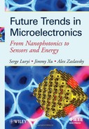
Figure 1. Band structure of QD rows.
In our previous publications,12,15,16 we considered structures with local barriers. Our main conclusions may be summarized as follows. The photocarrier lifetime critically depends on three factors: the ratio between the characteristic dot radius a and the electron mean free path /; the height of the potential barrier VM; and the heating of photocarriers by the electric field E. In the low electric field limit, if l> a, the photoelectron lifetime is given by: 12,16
where ND is the dot concentration and l/τε is the inelastic electron-phonon relaxation rate. The exponential factor describes the effect of potential barriers on capture processes.
In strong electric fields, on the other hand, photocarrier kinetics and transport are well described by the electron heating model. Our simulations show that the barriers strongly suppress capture processes until the average energy of carriers, i.e. the electron temperature, becomes comparable with the barrier height.12,16
To effectively suppress photoelectron capture, the barrier height VM should be at least 2–3kT. Such a local potential at room temperature means a dot should contain ten or more electrons.15 This requirement creates a lot of practical problems, such as high doping levels, specific large dot sizes, etc. Below, we shall focus on creating effective collective barriers in lateral and vertical structures.
4. QDIPs with lateral transport
A schematic QDIP with lateral photocarrier transport is shown in Fig. 2(a). A typical photodetector is based on the modulation-doped AlGaAs/GaAs with self-assembled InAs QDs. The QD layers are embedded in GaAs quantum wells of thickness of 2d, while the AlGaAs barriers are doped to supply the dots with electrons or holes.
A typical detector might contain ~10 QD layers to match the wavelength of interest. Ohmic contacts to the lateral QD structures are fabricated by depositing and annealing AuNiGe alloy. Because of the complex contact technology, the inter-electrode distance is relatively large: L ~ 100 μm. The corresponding band diagram of the structure is shown in Fig. 2(b). Potential barriers are created by the charged QD planes and charged planes of dopants. Photoexcited carriers move along areas with high mobility near the modulation-doping heterointerfaces. Thus, potential barriers between high-mobility conducting states and localized states in QDs are proportional to the distance d between the QD plane and AlGaAs barrier.
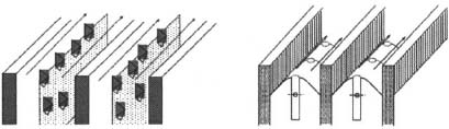
Figure 2. The QDIP with the lateral transport (a) and the corresponding band structure (b).
The photoelectron kinetics in such lateral structures was experimentally investigated at Τ = 77 K,17 with the result that the photocarrier lifetime and the detector responsivity depended exponentially on d. The lifetime was measured to be as long as 3 ms. The corresponding photoconductive gain gPH was evaluated as ~106. In this way, the critical importance of the collective potential barriers in lateral structures was fully confirmed by measurements at Τ = 77 K. At higher temperatures (~200 K), the QDIP performance deteriorated markedly because of the parasitic effects in Ohmic contacts.
We now turn to the theoretical performance limits of the lateral QDIPs at the room temperature by modeling photocarrier capture. Our Monte-Carlo program includes electron scattering on acoustic, polar optical, and intervalley phonons. We use the Γ–L–X model for simulation kinetics and transport in GaAs/AlGaAs structures with InAs dots.
Our results show that in small electric fields, the capture time exponentially increases with increasing of the height of the potential barrier VM. In the lateral structures, the potential is created by charged planes and it may be presented as VM = e2NDnd/(2εrε0) (see the inset in Fig. 3), where ND is the dot concentration in QD planes, and n is the dot occupation, i.e. the average number of carriers per dot. Thus, the capture time increases exponentially with dot concentration, occupation, and the well width d. In Fig. 3(a) we present the dependence of the capture time on the occupation n for typical parameters: ND = 4 x 1010 cm-2 and d = 80 nm. As in the case of QD structures with local barriers, the effect of the electric field can be understood in terms of the electron heating. The electric field increases the average energy (temperature) of carriers, so the barriers are less effective in preventing the capture of hot electrons. Therefore, the capture time decreases as the electric field increases. The detector responsivity is proportional to the photoconductive gain gPH, which is defined as a ratio of the photoelectron lifetime to the transit time ~ L/μΕ. Fig. 3(b) plots the dependence of the photoconductive gain on the electric field. The initial increase of gPH with E is due to the decrease of the transit time. The decrease of gPH in strong fields is due to a decrease in the capture time. Our modeling demonstrates that collective barriers increase the photoelectron lifetime and photoconductive gain in the room-temperature lateral QDIPs. While for the structures used in Ref. 17 this increase is not predicted to be sufficient for room-temperature applications, the effect can be significantly enhanced in QD structures with higher dot concentrations and larger values of the well width d.

Figure 3. (a) Capture time vs. dot carrier occupation n, barrier height VM is shown in the inset; (b) photoconductive gain vs. electric field.
5. QDIPs with vertically correlated dot clusters
The advantages of QWIPs with the vertical transport over the lateral QWIPs include a shorter intercontact distance and well-established processing technologies that promise high-quality reproducible Ohmic contacts. The short detector base decreases the generation-recombination noise and increases the photoconductive gain. High-quality Ohmic contacts are critical for both the detector responsivity and noise characteristics. To combine the advantages of the vertical QDIPs with barrier-limited capture, we propose a detector based on structures with vertically correlated dot clusters (VCDC).
A schematic of the VCDC structure is presented in Fig. 4. Positions of quantum dot clusters are correlated in the direction of the electric current, i.e. in the vertical direction. Thus, the correlated clusters of QDs form pancake-like structures. The collective barriers around QD clusters are created by charged dots. These barriers separate the conducting channels in the matrix from the localized states in quantum dots. Having been excited by radiation, photocarriers move in the areas between dot clusters through high-mobility conducting channels, as shown in Fig. 4. If the cluster radius b exceeds the distance between dot planes c, the barrier potential around clusters has a logarithmic form VM = e2Nn/(2πεrε0C) In(w/b), where N is the number of dots in the cluster, n is the average number of carriers per dot, and 2xv is the distance between the centers of two clusters.
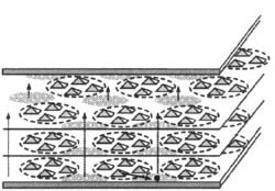
Figure 4. Structure with vertically correlated dot clusters (VCDCs).

Figure 5. (a) Capture time and the barrier height (inset) vs. dot occupation n; (b) photoconductive gain vs. electric field.
Results of the Monte-Carlo modeling of photocarrier kinetics in VCDC structures show that the capture time exponentially increases with increasing of the number of dots in a cluster N and the occupation n. At the same time, the capture processes are weakly sensitive to geometrical parameters w and b. Fig. 5(a) illustrates the exponential dependence of the capture time on the occupation of dots for N = 9, b = 75 nm, and w = 150 nm. We also investigate the dependence of the capture time on the electric field E, which is presented in Fig. 5(b). Again, this dependence is nonmonotonic due to electron heating effects.
Thus, the modeling shows that compared with ordinary quantum-dot structures, where the photoelectron lifetime at room temperatures is of the order of 1–10 ps, the VCDC structure with collective potential barriers would allow for increasing the photocarrier lifetime by up to three orders of magnitude.
6. Conclusions
Long photocarrier lifetime is a key issue for improving of room-temperature infrared photodetectors. Detectors based on quantum dot structures permit the engineering of specific properties and hence hold promise of overcoming the limitations of quantum well detectors. In this chapter we reviewed photocarrier kinetics in traditional QDIPs and presented the modeling of the capture processes in the lateral structures and vertical structures with vertically correlated dot clusters. The results show that QDIPs can substantially outperform QWIPs due to manageable photocarrier kinetics, which can be controlled by potential barriers created by dot clusters. Modern technologies allow the fabrication of various structures with the correlated QD clusters. Detailed modeling of such structures will pave the way for optimal design of the room-temperature QDIPs.
Acknowledgments
This work was supported by an AFOSR contract.
References
1. M. Razeghi, H. Lim, S. Tsao, J. Szafraniec, W. Zhang, K. Mi, and B. Movaghar, “Transport and photodetection in self-assembled semiconductor quantum dots,” Nanotechnology 16, 219 (2005).
2. J. C. Campbell and A. Madhukar, “Quantum dot infrared detectors,” IEEE J. Quantum Electronics 95, 1815 (2007).
3. A. V. Barve, S. J. Lee, S. K. Noh, and S. Krishna, “Review of current progress in quantum dot infrared photodetectors,” Laser & Photonics Reviews, June 17, 2009.
4. B. F. Levine, “Quantum-well infrared photodetectors,” J. Appl. Phys. 74, Rl (1993).
5. E. A. Zibik, T. Grange, B. A. Carpenter, et al., “Long lifetimes of quantum-dot intersublevel transitions in the terahertz range,” Nature Mater. 8, 803 (2009).
6. V. Ryzhii, “The theory of quantum-dot infrared phototransistors,” Semicond. Sci. Technol. 11, 759(1996).
7. U. Bockelmann and G. Bastard, “Phonon scattering and energy relaxation in two-, one-, and zero-dimensional electron gases,” Phys. Rev. B 42, 8947 (1990).
8. Y. Toda, O. Moriwaki, M. Nishioka, and Y. Arakawa, “Efficient carrier relaxation mechanism in InGaAs/GaAs self-assembled quantum dots based on the existence of continuum states,” Phys. Rev. Lett. 82, 4114 (1999).
9. R. Ferreira and G. Bastard, “Phonon-assisted capture and intradot Auger relaxation in quantum dots,” Appl. Phys. Lett. 74, 2818 (1999).
10. P. Bhattacharya, X. H. Su, S. Chakrabarti, G. Ariyawansa, and A. G. U. Perera, “Characteristics of a tunneling quantum-dot infrared photodetector operating at room temperature,” Appl. Phys. Lett. 86, 191106 (2005).
11. S. Tsao, H. Lim, W. Zhang, and M. Razeghi, “High operating temperature 320×256 middle-wavelength infrared focal plane array imaging based on an InAs/InGaAs/InAlAs/InP quantum dot infrared photodetector,” Appl. Phys. Lett. 90, 201109(2007).
12. L.-H. Chien, A. Sergeev, N. Vagidov, and V. Mitin, “Hot-electron transport in quantum-dot photodetectors,” Intern. J. High Speed Electronics Syst. 18, 1013 (2008).
13. J. Phillips, “Evaluation of the fundamental properties of quantum dot infrared detectors,” J. Appl. Phys. 91, 4590 (2002).
14. P. Martyniuk and A. Rogalski, “Quantum-dot infrared photodetectors: Status and outlook,” Prog. Quantum Electronics 32, 89 (2008).
15. A. Sergeev, V. Mitin, and M. Stroscio, “Quantum-dot photodetector operating at room temperatures: Diffusion-limited capture,” Physica B 316-317, 369 (2002).
16. V. Mitin, A. Sergeev, L.-H. Chien, and N. Vagidov, “High performance of IR detectors due to controllable kinetics in quantum-dot structures,” Proc. SPIE 7095, 70950K (2008).
17. K. Hirakawa, S.-W. Lee, Ph. Lelong, et al., “High-sensitivity modulation-doped quantum dot infrared photodetectors,” Microelectronic Eng. 63, 185 (2002).