
Semiconductor Scintillator for Three-Dimensional Array of Radiation Detectors
Dept. of Electrical and Computer Engineering, SUNY-Stony Brook Stony Brook, NY 11794-2350, U.S.A.
1. Introduction
There are two large groups of solid-state radiation detectors that dominate the area of ionizing radiation measurements: scintillation detectors and semiconductor diodes. The scintillators detect high-energy radiation through generation of light, which is subsequently registered by a photodetector that converts light into an electrical signal. Semiconductor diodes employ reverse biased pn junctions where the absorbed radiation creates electrons and holes, which are separated by the junction field thereby producing a direct electrical response. Both groups of detectors are extensively reviewed in the classical treatise by Knoll.1
Most scintillators reported in the literature are implemented in wide-gap insulating materials doped (“activated”) with radiation centers. A classic example of a solid-state scintillator is sodium iodide activated with thallium (NaI:Tl), introduced by Hofstadter2 more than 60 years ago.
The typical band diagram of a solid-state scintillator is shown in Fig. 1. Because of the much longer wavelength of the scintillation associated with the activator energy levels – compared to the interband absorption threshold – the insulating scintillators are very transparent to their own luminescence. However, this advantage comes at a price in the transport of carriers to the activator site. Individual carriers have very poor mobility in insulators and transport efficiency requires that the generated electrons and holes form excitons and travel to the radiation site as neutral entities. Therein lies a problem. The energy resolution even in the best modern scintillators does not compare well with that in semiconductors.4 One of the fundamental reasons for poor resolution is that the luminescent yield in dielectric scintillators is controlled by reactions that are nonlinear in the density of generated electron-hole pairs, such as the formation of excitons at low densities and the Auger recombination at high densities.5-8
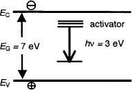
Figure 1. Conventional solid-state scintillator. Schematic energy band diagram of the thallium activated sodium iodide. Electrons and holes generated across the bandgap EG migrate to the nearest activation site and recombine there, emitting much lower photon energy hv .
It is important to stress that such nonlinear processes do not exist in direct-gap doped semiconductors, where interaction with gamma radiation induces minority carriers, while the concentration of majority carriers does not measurably change. Every reaction on the way to luminescence, including Auger recombination, is linear with respect to the concentration of minority carriers. One can therefore expect, as a matter of principle, that doped semiconductor scintillators will not exhibit effects of non-proportionality and their ultimate energy resolution could be on par with that of diode detectors implemented in the same material.
Normally, scintillators are not made of semiconductor material. The key issue in implementing a semiconductor scintillator is how to make the material transmit its own infrared luminescence, so that photons generated deep inside the semiconductor slab could reach its surface without tangible attenuation. However, semiconductors are usually opaque at wavelengths corresponding to their radiative emission spectrum. Our group has been working on the implementation of high-energy radiation detectors based on direct-gap semiconductor scintillator wafers, like InP or GaAs. For the exemplary case of InP, the scintillation spectrum is a band of wavelengths near 920 nm. The original idea was to make InP relatively transparent to this radiation by doping it heavily with donors, so as to introduce the Burstein shift between the emission and the absorption spectra.9 Because of the heavy doping, the absorption edge is blue-shifted relative to the emission edge by the carrier Fermi energy. Unfortunately, the Burstein shift by itself does not seem to provide adequate transparency at room temperature, so the signal is attenuated depending on the depth of the interaction site within the semiconductor. The problem is discussed in Section 3 and its resolution in Section 4.
The transparency issue is of critical importance and we are concerned with new ways to further enhance the photon delivery to the semiconductor surface. One of the key new ideas is discussed in this paper. It is based on the extremely high radiative efficiency of high-quality direct-gap semiconductors. This means that an act of interband absorption does not finish off a scintillation photon; it merely creates a new minority carrier and then a new photon in a random direction. The efficiency of photon collection in direct-gap semiconductors is therefore limited only by parasitic processes, such as nonradiative recombination of the minority carriers and free-carrier absorption of light. The “ideal” semiconductor scintillator based on photon recycling is discussed in Section 5.
The proportionality of scintillation yield is not the only expected advantage of semiconductor scintillators. One of the major benefits of using semiconductor materials is the mature technology that enables the implementation of epitaxial photodiodes integrated on the surface of a semiconductor slab. An external receiver, like a photomultiplier, is not a viable option because of the complete internal reflection of most of the scintillating radiation. Owing to the high refractive index of semiconductors, e.g. η = 3.3 for InP, most of the scintillating photons will not escape from the semiconductor but suffer complete internal reflection. Only those photons that are incident on the semiconductor-air interface within a narrow cone sine < 1/n from the interface normal have a chance to escape from the semiconductor. The escape cone accommodates only a small fraction of isotropic scintillation, sin2(θ/2) < l/4n2 ~ 2%, leading to inefficient collection.
It is therefore imperative to integrate the scintillator wafer with a photodetector that has a substantially similar or even higher refractive index in an optically tight fashion. In collaboration with Sarnoff Corporation, our group has achieved substantial progress with epitaxial photodetectors on InP scintillator body, implemented as ultra-low leakage pin diodes based on quaternary InGaAsP materials.10 These material layers of 1.24 eV bandgap are grown epitaxially on lattice-matched InP scintillator body and are sensitive to InP scintillation at the wavelength of 0.92 μm (hν = 1.35 eV). The epitaxial diode provides nearly perfect registration efficiency of photons that have reached the heterointerface. This in turn enables three-dimensional (3D) integration of scintillator “voxels” (3D pixels) that is illustrated in Fig. 2 and discussed in the next section (Section 2).
2. Three-dimensional array of scintillator voxels: A Compton telescope
A stack of individually contacted 2D pixellated semiconductor slabs forms a 3D array of scintillator voxels, as illustrated in Fig. 2. This is the key concept of interest to us. A gamma photon incident on such an array undergoes several Compton interactions depositing varying amounts of energy Δi in voxels with coordinates ri = (xi, yi, zi). The information reported enables one to determine both the incident photon energy and the direction to the source.

Figure 2. Schematic illustration of a 3D scintillator array. Each unit is a voxel comprising a scintillator body (white slab) and an integrated photodiode (top plate) on its surface. Advantageously, the voxel may include two photodiodes integrated on both surfaces in an optically tight fashion. An incident gamma photon produces a cluster of firing pixels that report their positions and the energy deposited. The information can be used to determine both the incident photon energy and the source direction. The diagram illustrates the track of a gamma photon of diminishing energy upon several successive Compton interactions producing a cluster of firing voxels.
The exact relativistic kinematics of Compton scattering provides two equations at each interaction site, illustrated in the diagram in Fig 2:
where all energies are expressed in units of electron rest energy, mec2 = 511 keV. With three points ri, identified in the correct order (i = 1, 2, 3) the set of equations (1) enables one to deduce both the incident energy and the incident direction cosine from the known energies Δ1 and Δ2 deposited in the first two pixels and the direction θ2 to the third pixel, as shown in Fig. 2. Direction-wise, the point source is placed on the cone of angle θ1 about the measured direction n1. Intersection of two or three such measurements gives the direction to the source. This technique is known as the Compton telescope.11-13
In contrast to gamma spectroscopy by conventional non-pixellated detectors,1 a 3D array does not need to capture the entire incident gamma photon energy E0 in order to determine E0. However, the technique works only to the extent that one can order the events. Measurement of a fourth point in the cluster adds two equations and only one unknown and therefore can be used to determine the correct sequence. If all the measured quantities had a mathematical precision, the system of equations would be consistent only for the correct order. In practice, because both the positions and energies are measured only to within a certain margin of accuracy, the determination of the best order (referred to as the tracking algorithm or the event reconstruction) becomes a statistical procedure that minimizes inconsistency. Current tracking algorithms claim up to 70% success in correctly ordering events produced by a high-energy photon, by including in the analysis, besides the Compton kinematics, the anisotropic scattering cross-sections, expressed by the well-known1 Klein-Nishina formula.
Semiconductor scintillators offer a tantalizing possibility of implementing a compact low-voltage Compton telescope.

Figure 3. Schematic band diagram of a direct-gap semiconductor scintillator based on the Burstein shift (after Ref. 9). The semiconductor (InP) is doped n-type with degenerate doping concentration ND < 1018 cm-3. The minority carriers (holes) are expected to recombine radiatively with electrons at the bottom of the Fermi sea. Absorption of thus emitted photons is largely suppressed.
3. Problems with scintillator based on Burstein shift
The original idea of Burstein-shift based scintillator9 is illustrated in Fig. 3. Thermalized minority carriers (holes) are distributed near the top (within kT) of the valence band occupying a narrow range of wavenumbers ħk ~ (2mhkT)12. Conservation of momentum in radiative transitions requires that participating electrons have the same wavenumber and leads to an expected spectrum of emitted photons hv ~ EG + ΔE of width ΔΕ ~ kT(mh/me + 1). However, experimentally the emission spectrum S(E) of heavily-doped InP is wider (of width about EF > ΔΕ) and it does not substantially narrow at cryogenic temperatures. This suggests that, in our heavily-doped samples, momentum is not conserved and the entire Fermi sea of electrons contributes to the spectrum, as illustrated in Fig. 4.
The Burstein shift does provide an enhanced transparency but it has not proven sufficient for the intended application. In n-type InP with donor concentration of ND = 6×l018 cm-3 at room temperature, the mean free path of photons averaged over the fundamental emission spectrum is about 100 μm. That is obviously not enough. However, InP has a high radiative efficiency η (over 90%) and those photons that are absorbed generate another electron-hole pair that recombines producing a new photon. We shall discuss this photon recycling process in more detail in Section 3. At this point, however, it can be noted that once photon recycling becomes a key mechanism, heavily-doped samples are no longer necessarily the best. The optimum doping concentration is set by (i) free-carrier optical absorption that obviously favors low doping; (ii) radiative efficiency, which depends on the dominant mechanism of nonradiative recombination; and (iii) the transparent fraction of the spectrum S(E) that may benefit from the Burstein shift.
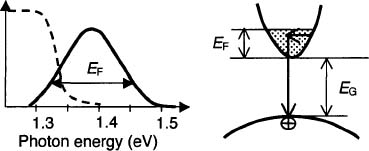
Figure 4. Schematic illustration of spectra S(E) observed in heavily-doped InP (solid line). The dashed line indicates the transparency of the sample (on a logarithmic scale). The right-hand panel illustrates the radiative transitions that do not conserve quasi-momentum in heavily-doped material.
Photon recycling can deliver a reasonable fraction of the scintillating photons to the wafer surface. However, this fraction depends on the exact position of the interaction site relative the surface and this constitutes a major problem for the accurate determination of the deposited energy. One needs to distinguish the signal arising from a large energy deposited far from the photoreceiver surface from that arising from smaller energy deposited nearby.
The problem arises from the attenuation of the optical signal. If we knew the distance z of the gamma interaction event from the photoreceiver surface, one could correct for the attenuation. Recently, we came up with a method for accomplishing this, based on two-sided photodetection using epitaxial photodiodes on both sides of the InP scintillator wafer.14 The simultaneous detection by both detectors of the scintillation arising from the same interaction event, allows us to determine the position of the interaction and therefore correct for attenuation.
4. Double-sided detection
Consider a scintillator slab shown in Fig. 5, with two arrays of photodetectors and two read-out circuits on the opposite sides of the slab. An essential ingredient of the proposed approach is the ability to extract the event position, characterized by a distance z the top surface, by analyzing two photoreceiver signals from the same ionization event. Our calculations indicate that it is sufficient to know the ratio of the two signals to accurately estimate of the event position. Another essential ingredient is the ability to correct for the attenuation after the position has been ascertained. Both of these capabilities can be obtained by calculations coupled with experimental validation.

Figure 5. Schematic cross-section of an InP scintillator with two epitaxial InGaAsP photodiodes grown on both sides. Exemplarily, d = 350 μm, while the thickness of epitaxial diodes is ~2 μm (exaggerated in the figure). Lateral dimensions of the scintillator are about 1 mm.
In heavily doped InP the attenuation is due to losses - of photons due to free-carrier absorption and minority carriers due to nonradiative recombination. However, the ratio of attenuated signals is not sensitive to these losses, see Sect. 5.
Suppose an interaction event occurs at a distance z from the top surface (see Fig. 5). As a result, both the top and the bottom photodetectors will produce a signal. The calculated ratio p(z) = D2/D1 of these two signals is plotted in Fig. 6 for different scintillator doping levels. It is assumed that the photodiodes themselves are ideal and identical on both sides. Fig. 6 shows that simultaneous measurement of the responses D1 and D2 gives sufficient information to locate the position z of the interaction event.
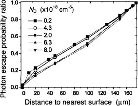
Figure 6. Calculated (see Eq. (10) in text) ratio of the two signals recorded by two surface detectors for the same radiation event for different doping levels in the scintillator body. The scintillator thickness is d = 350 μm as in Fig. 5, and the ratio is shown for z ≤ d/2, since ρ(z) = ρ-1d–z) by symmetry.
5. Scintillator based on photon recycling
In high-quality direct-gap semiconductors, most of the scintillation photons reaching the detectors’ surface are not photons directly generated by the electrons and holes at the site of the gamma particle interaction, but photons that have been re-absorbed and re-emitted a multiple number of times. This phenomenon, known as photon recycling, was introduced by Dumke15 and Moss16 and used by Asbeck17 to explain the long radiative lifetime in GaAs/AlGaAs heterostructures. It is often discussed in connection with high-efficiency light emitting diodes.18 It is essential for understanding the properties of our direct-gap semiconductor scintillator.
Traditionally, an ideal scintillator requires material that is highly transparent to its own luminescence. For example, one can imagine doping the semiconductor with high efficiency radiative centers that emit below-bandgap light. It is important that the excited electron-hole pairs are efficiently transferred to the radiative center. In the case of InP, this energy transfer probability was shown19 to be high for certain trivalent luminescent ions incorporated in the host lattice. The system InP:Yb3+ seems to work well at cryogenic temperatures, producing emission near 1 μm – well below the bandgap of InP. However, at room temperature, its performance is degraded by fast nonradiative de-excitation of Yb ions.19 Other ideas for implementing transparent semiconductor scintillators include replacing luminescent ions by semiconductor “impregnations” of lower bandgap.20
In the presence of multiple photon recycling one can have another kind of ideal {nontransparent but lossless) scintillator, as we shall now discuss.
Let the luminescent signal comprise the energy spectrum S(E) =GS0(E) (where S0 is normalized to unity, ![]() s0(E)dE = 1). The signal is assumed to be generated a distance z from the detector top surface, as indicated in Fig. 5. The emitted energy is isotropic, so that the energy emitted in unit energy interval per unit solid angle is (G/4π)S0(E). The total energy Di(z) reaching the ith detector surface (i’ = 1, 2) is attenuated in a way that depends on z.
s0(E)dE = 1). The signal is assumed to be generated a distance z from the detector top surface, as indicated in Fig. 5. The emitted energy is isotropic, so that the energy emitted in unit energy interval per unit solid angle is (G/4π)S0(E). The total energy Di(z) reaching the ith detector surface (i’ = 1, 2) is attenuated in a way that depends on z.
In the presence of absorption, characterized by the interband absorption coefficient αi(E), the detection probability for a photon at energy E (averaged over all angles) is given by
where ρ = ztanθ and r = z/cosθ. Averaged over the emitted photon spectrum S(E), the probability p1 that the photon reaches detector 1 at z = 0 is given by
We shall refer to the probability (5) and the similar probability p2(z) = p1(d–z) that the photon generated at point z reaches detector 2 at z = d, as single-pass probabilities, because they do not include the subsequent fate (recycling) of the absorbed photon. The probability (5), calculated using experimental spectra S(E) for different doping levels in InP, is shown in Fig. 7.

Figure 7. Single-pass photon escape probability p1(z) calculated for a 350 μm InP layer, doped n-type at different doping levels. The probabilities are plotted vs. distance from the interaction site to the integrated photodiode surface. The calculation is based on measurements of the absorption spectra in these crystals.
The single-pass probability pFCA of free-carrier absorption (FCA) describes the importance of these parasitic lossy processes relative to interband absorption. It can be estimated by neglecting both p1 and p2, while keeping the dominant process of interband absorption,
where αe(E) is the FCA absorption coefficient, primarily owing to intervalley electronic transitions.19 Both αi and αe depend on the doping level, the former through the Burstein shift and the latter because it is directly proportional to the number of majority carriers.
Consider the basic processes in an InP scintillator with two photodiode surfaces, as in Fig. 5. The minority carrier (“hole” h) initially created by the ionizing interaction has the probability η (radiative efficiency) to generate a photon (of energy spectrum 5). The generated photon can either reach detector 1 or 2 (designated by probabilities p1 and p2, respectively) or disappear through FCA (with probability pFCA). All these probabilities depend on the position z (the spectral dependence can be eliminated by averaging over S). The combined probability P(z) = p1+p2+pFCA describes the likelihood of the photon loss at this stage, and the alternative, 1 – P(z), is the probability that a new hole is created through interband absorption. The cycle of hole-photon-hole transformation repeats ad infinitum, as illustrated in the diagram in Fig. 8.

Figure 8. Schematic diagram of the basic processes in an InP scintillator with two photodiode surfaces.
So long as the photon recycling process continues, the minority carriers (holes) and photons are interchangeable entities. While the entity is a photon, the process can be finished off by FCA (with the probability pFCA), whereas while the entity is a hole it can be ended by a nonradiative transition that occurs with the small probability ξ = 1 – η (in our samples η ranges from 90% to 99%). Needless to say, the process can also have a happy end (photon detected). The radiative efficiency is defined in terms of the rates of radiative (νR) and nonradiative (νNR) transitions:
The total signal in detector 1 is a sum of the single-pass contributions from different cycles of photon regeneration. As is evident from Fig. 8, it can be summed as a geometric progression, giving:
Similarly, the total signal in detector 2 is given by
Equations (8) and (9) express the attenuated signal in terms of single pass probabilities and photon recycling parameters η and pFCA. However, the ratio of the two signals,
depends only on the single-pass probabilities given by the spectral dependence of the interband absorption only, as is evident from Eqs. (4) and (5). The calculated signal ratio (10) with pi and p2 as in Fig. 7, was plotted in Fig. 6 above.
It is important to note that for high photon recycling (η → 1 and pFCA → 0), one has an ideal scintillator in the sense that all generated photons are collected -even though the single-pass probabilities p1 and p2 may not be high due to interband absorption. However, the interband absorption does not “kill off the photon because another minority carrier is created. In a sample with high η another photon will reemerge to make a new try at reaching one of the detectors. If the FCA is also low, all photons will be eventually collected in this way.
Let us emphasize that in such an ideal scintillator the ratio of signals will still depend on the position ζ of the interaction, as shown by Eq. (10). This extends the validity of the two-sided detection concept to the case of a perfect scintillator based on photon recycling. In the case of such a perfect scintillator, the value of two-sided detection is not only that it doubles the overall number of photons collected, but it also provides the position identification not limited to the vertical dimension of the pixel. One can have a thick pixel and still resolve the vertical position from the pre-calibrated ratio (10).
An important parameter for scintillator applications in gamma-spectroscopy is the photon collection efficiency (PCE),
The PCE is generally less than unity, due to the above-discussed loss processes. From Eqs. (8) and (9) we find that the total PCE is given by:
6. How close are we to an ideal semiconductor scintillator?
As is clear from Eq. (12), implementation of an ideal scintillator based on photon recycling requires: (a) high radiative efficiency (η → 1 or νNR/νR ![]() 1); (b) low free-carrier absorption (pFCA → 0); and (c) reasonable transparency, expressed by nonvanishing single-pass probabilities, p1(z) + p2(z) ≥ 2p1(d/2).
1); (b) low free-carrier absorption (pFCA → 0); and (c) reasonable transparency, expressed by nonvanishing single-pass probabilities, p1(z) + p2(z) ≥ 2p1(d/2).
Optimization of the condition (a) depends on the nature of nonradiative recombination. The total minority-carrier recombination rate is given by
where n is the majority-carrier concentration provided by the doping (n = ND at room temperature). The first term A describes a nonradiative mechanism due to unintended acceptor-like impurities, whose concentration NA (and hence νNR) is independent of ND, term B describes the radiative rate νR, and term C describes the Auger nonradiative recombination mechanism.
If the dominant nonradiative mechanism is A, then one would expect the optimum to be at higher ΝD, since the radiative rate νR ~ ND. If, on the other hand, the dominant nonradiative mechanism is due to Auger recombination (νNR ~ ND2), then one should seek the optimum at lower ΝD.
Our experimental results clearly favor the Auger mechanism, see Fig. 9. The solid line is a fit to the recombination rates given by Eq. (13), with the radiative (B) and Auger (C) coefficients taken from our luminescence experiments (these are close to the room-temperature date reported in the literature,22 within their margin of accuracy) and a fitted coefficient A. The lower-doped samples have evidently higher radiative efficiency, with a maximum of about 99% at ND ≈ 2×l017 cm-3. At still lower concentrations, one can expect η to drop due to term A.
Condition (b) is clearly favored by lower doping concentrations, cf. Fig. 10. For ΝD ≈ 2×l017 cm-3, the FCA absorption is very small, αe < 0.1 cm-1, and the probability pFCA can be neglected.
Finally, condition (c) – which had been the key consideration at the start of our work – depends primarily on the positioning of the interband absorption spectrum αi(E) relative to the basic luminescence emission spectrum S(E), as evident from Fig. 4 and Eqs. (4) and (5). This is precisely the condition that we had sought to optimize with the Burstein shift. However, our theoretical considerations had led us to consider much lower concentration ranges, where the Burstein shift is inoperative. The experimentally observed luminescence spectra show that the low-doped (non-degenerate) sample with ND = 2×1017 cm-3 is about ten times brighter than our best degenerately doped samples. In the low-doped sample both the quantum efficiency becomes high (due to the absence of Auger recombination) and the residual (free-carrier) absorption becomes very low. The feared drawback of lower-doped samples, the tight overlap of the absorption and emission bands, is more than compensated by high photon recycling.

Figure 9. Room-temperature radiative efficiency as function of majority-carrier concentration provided by the doping ND. The solid line describes a fit to Eq. (13) with A = 2×10⁵ s-1 B= 1.9×10⁻¹⁰cm3/s, and C = 1.5×10⁻³⁰ cm6/s.

Figure 10. Free-carrier absorption coefficient αe vs. ND measured in our inP samples. At the lowest concentration ND = 2×1017 cm-3, one has αe < 0.1 cm-1.
Once the conditions (a–c) are satisfied, the photon collection efficiency predicted by Eq. (12) is very high indeed, even when single-pass probabilities are low. With negligible free-carrier absorption (PFCA → 0) and the high radiative efficiency (νNR/νR = 0.01) featured by our low-doped InP samples, the PCE = 0.95 assuming p1(z) + p2(z) ~ 0.2, as estimated from our earlier experimental data. Even for still lower single-pass probabilities, such as 2p1(d/2) ≈ 0.1, estimated theoretically (see Fig. 7), one has PCE = 0.91. It should be noted that the theoretical estimate presented here gives a lower estimate for the PCE. A more detailed theoretical analysis, now in progress, will allow for (i) finite size of the initial excitation region, and (ii) expansion of the excitation region in the process of recycling. Both effects are expected to increase the PCE estimate. Inclusion of (i) is reasonably straightforward, provided one knows the spatial distribution H(r) of holes generated by the gamma photon. One would then simply average Eqs. (8) and (9) over H(r). Evaluation of H(r) is not a simple matter, however.23,24
Inclusion of the effect (ii) is more subtle, especially for the lower-doped samples. Our derivation of Eqs. (8) and (9) assumes that every act of recycling occurs at the same place z where the initial interaction occurred, and therefore the same probabilities p1(z) and p2(z) appear at all stages of the recycling, see Fig. 8. This has reduced the summation of an infinite series to a geometric progression and allowed us to obtain the result in a closed form. In reality, however, there is a transport of holes in photon recycling, which has the nature of a random walk. Recombination of a hole at a position r is accompanied by the emergence of another hole at a r + l, where l is a random vector, characterizing the free flight of an emitted photon. In a heavily doped sample this random walk reduces to diffusion with a diffusion coefficient ~|f|2/τ, where τ is the radiative recombination time. For a sample with ND = 6×l018 cm-3 we estimate |l| to be of order 100 μm. For lightly-doped samples, however, the diffusion approximation breaks down because of the extreme transparency in the long wavelength wing of the spectrum S(E), where |l| is limited by FCA only. For the sample with ΝD ≈ 2×l017 cm-3, where αe < 0.1 cm-1, one has αed![]() 1, and nothing should change if we set αe= 0, which corresponds to diverging free flight |l| → ∞. Random walks with a distribution of unit flights so long-tailed that their second moment diverges are known as Levy flights.25 An interesting example of optical Levy flights was recently discussed by Barthelemy et al.26 Such random walks with divergent average step length lead to the so-called super-diffusion, where the average squared displacement increases superlinearly with time. As subtle as this may be, the super-diffusive behavior is likely to be of importance for estimating the photon collection efficiency. By a crude analogy with averaging over H(r), we expect that the single-pass probabilities in Eq. (12) will be replaced by larger “effective” values p′i(z) > pi(z), further enhancing the PCE estimate. The enhancement is hard to predict at this time and it requires further studies. The ultimate aim of these studies is an accurate estimate of the optimum scintillator layer thickness for best energy resolution.
1, and nothing should change if we set αe= 0, which corresponds to diverging free flight |l| → ∞. Random walks with a distribution of unit flights so long-tailed that their second moment diverges are known as Levy flights.25 An interesting example of optical Levy flights was recently discussed by Barthelemy et al.26 Such random walks with divergent average step length lead to the so-called super-diffusion, where the average squared displacement increases superlinearly with time. As subtle as this may be, the super-diffusive behavior is likely to be of importance for estimating the photon collection efficiency. By a crude analogy with averaging over H(r), we expect that the single-pass probabilities in Eq. (12) will be replaced by larger “effective” values p′i(z) > pi(z), further enhancing the PCE estimate. The enhancement is hard to predict at this time and it requires further studies. The ultimate aim of these studies is an accurate estimate of the optimum scintillator layer thickness for best energy resolution.
7. Conclusions
As discussed in the introduction, the semiconductor scintillator does not suffer from the non-proportionality effects and its energy resolution is fundamentally limited by energy branching in the same way as it is for semiconductor diodes. However, high photon collection efficiency is an obvious prerequisite for the good energy resolution. We have shown that a semiconductor scintillator based on photon recycling is capable of delivering very high PCE, even though the material is not transparent in the usual sense to its own luminescence. In order to take advantage of photon recycling, double-sided integrated photodiodes appear necessary. We can ultimately expect the energy resolution of semiconductor scintillators to approach that of a diode detector implemented in the same material.
Acknowledgments
This book chapter would not be possible without the contributions of the radiation detector research group at Stony Brook University, including Alex Kastalsky, Michael Gouzman, Nadia Lifshitz, Oleg Semyonov, Milutin Stanacevic, and Vladislav Kuzminsky, and graduate students William Cheng, Vladimir Smagin and Zhichao Chen. We would also like to acknowledge important contributions of our friends and collaborators at Sarnoff Corporation, Joseph Abeles, Winston Chan and Zane Shellenbarger.
This work was supported by the Domestic Nuclear Detection Office (DNDO) of the Department of Homeland Security, by the Defense Threat Reduction Agency (DTRA) through its basic research program, and by the New York State Office of Science, Technology and Academic Research (NYSTAR) through the Center for Advanced Sensor Technology (Sensor CAT) at Stony Brook.
References
1. G. F. Knoll, Radiation Detection and Measurement, 3rd ed., New York: Wiley, 2000.
2. R. Hofstadter, “Alkali halide scintillation counters,” Phys. Rev. 74, 100 (1948).
3. C. L. Melcher, “Perspectives on the future development of new scintillators,” Nucl. Instrum. Methods Phys. Res. A 537, 6 (2005).
4. P. Dorenbos, “Light output and energy resolution of Ce3+-doped scintillators,” Nucl. Instrum. Methods Phys. Res. A 486, 208 (2002).
5. A. N. Vasil’ev, “From luminescence nonlinearity to scintillation non-proportionality,” IEEE Trans. Nucl. Sci. 55, 1054 (2008).
6. G. Bizarri, W. W. Moses, J. Singh, A. N. Vasil’ev, and R. T. Williams, “An analytical model of nonproportional scintillator light yield in terms of recombination rates,” J. Appl. Phys. 105, 044507 (2009).
7. G. Bizarri, W. W. Moses, J. Singh, A.N. Vasil’ev, and R. T. Williams, “The role of different linear and nonlinear channels of relaxation in scintillator non-proportionality,” J. Luminescence, in press (2009).
8. S. A. Payne, N. J. Cherepy, G. Hull, J. D. Valentine, W. W. Moses, and W.-S. Choong, “Nonproportionality of scintillator detectors: Theory and experiment,” IEEE Trans. Nucl. Sci. 56, 2506 (2009).
9. A. Kastalsky, S. Luryi, and B. Spivak, “Semiconductor high-energy radiation scintillation detector,” Nucl. Instrum. Methods Phys. Res. A 565, 650 (2006).
10. S. Luryi, A. Kastalsky, M. Gouzman, N. Lifshitz, O. Semyonov, M. Stanacevic, A. Subashiev, V. Kuzminsky, W. Cheng, V. Smagin, Z. Chen, J. H. Abeles, W. K. Chan, and Z. A. Shellenbarger, “Epitaxial InGaAsP/InP photodiode for registration of InP scintillation,” to be published.
11. E. Aprile, A. Bolotnikov, D. Chen, and R. Mukherjee, “A Monte Carlo analysis of the liquid xenon TPC as gamma-ray telescope,” Nucl. Instrum. Methods Phys. Res. A 327, pp. 216–221 (1993).
12. J. D. Kurfess, W. N. Johnson, R. A. Kroeger, and B. F. Phlips, “Considerations for the next Compton telescope mission,” Proc. 5th Compton Symp., Portsmouth, NH (1999).
13. S. E. Boggs and P. Jean, “Event reconstruction in high resolution Compton telescopes,” Astron. Astrophys. Suppl. Ser. 145, 311 (2000).
14. J. H. Abeles and S. Luryi, “Slab scintillator with integrated two-sided photoreceiver,” U.S. prov. patent application, Ser. No. 61/216,572 (2009).
15. W. P. Dumke, “Spontaneous radiative recombination in semiconductors,” Phys. Rev. 105, 139(1957).
16. T. S. Moss, “Theory of the spectral distribution of recombination radiation from InSb,” Proc. Phys. Soc. B 70, 247 (1957).
17. P. Asbeck, “Self-absorption effects on the radiative lifetime in GaAs/AlGaAs heterostructures,” J. Appl. Phys. 48, 820 (1977).
18. See, for example, R. Windisch, C. Rooman, B. Durta, Α. Knobloch, G. Borghs, G. H. Döhler, and P. Heremans, “Light-extraction mechanisms in high-efficiency surface-textured light-emitting diodes,” IEEE J. Selected Topics Quantum Electronics 8, 248 (2002).
19. A. Taguchi and K. Takahei, “Trap level characteristics of rare-earth luminescence centers in III-V semiconductors,” J. Appl. Phys. 79, 4330 (1996).
20. S. Luryi, “Impregnated semiconductor scintillator,” Intern. J. High Speed Electronics Syst. 18, 973 (2008).
21. W. P. Dumke, M. R. Lorenz, and G. D. Pettit, “Intra- and interband free-carrier absorption and the fundamental absorption edge in n-type InP,” Phys. Rev. B 1, 4668(1970).
22. See the electronic archive on semiconductor materials, characteristics and properties at http://www.ioffe.rssi.ru/SVA/NSM/, maintained by the Ioffe Physico-Technical Institute.
23. E. Gros d’Aillon, J. Tabary, A. Glière, and L. Verger, “Charge sharing on monolithic CdZnTe gamma-ray detectors: A simulation study,” Nucl. Instrum. Methods Phys. Res. A 563, 124 (2006).
24. J. Hayward and D. Wehe, “Incomplete charge collection in an HPGe double-sided strip detector,” Nucl. Instrum. Methods Phys. Res. A 586, 215 (2008).
25. See, for example, R. Metzler, A. V. Chechkin, V. Yu. Gonchar, and J. Klafter, “Some fundamental aspects of Levy flights,” Chaos, Solitons, Fractals 34, 129 (2007).
26. P. Barthelemy, J. Bertolotti, and D. S. Wiersma, “A Levy flight for light,” Nature 453, 495 (2008).