The Future of Microelectronics is ... Macroelectronics
Dept. of Electrical and Computer Engineering, Purdue University West Lafayette, IN 47906-3800, U.S.A.
1. Introduction
The title is actually not as provocative as it might seem. No one debates the miraculous success of microelectronics - enshrined in Moore’s law and iconified by Pentium chips – in transforming how we compute and communicate. Even as the technology – buffeted by many fundamental limits - slides into a more mature phase, the degree of miniaturization of transistors continues to amaze, e.g., the number of transistors made in a year by Intel or TSMC exceeds the estimates of ants or leaves in the world! Yet, the most exciting trends in electronics today are defined not by computers, but by flat panel displays, solar cells, and bioelectronics sensors. Sizing the solar cells, batteries or flat panel TV to the dimension of a Pentium is obviously counterproductive, if fact for such systems – the bigger, the better. If we categorize the electronics of flat-panel displays, energy conversion and conservation devices as being macro- or large-scale electronics1 (see Fig. 1), presumably few would quibble with the title of the article that “the future of microelectronics lies with macroelectronics”.2,3
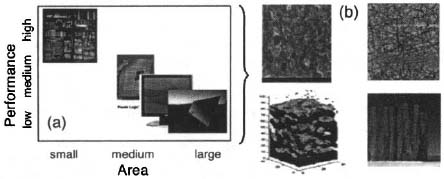
Figure 1. (a) Traditional microelectronic ICs emphasize high performance with small footprint (top, left), but macroelectronic devices like displays and energy conversion devices favor large area devices with low to moderate performance (bottom, right), (b) Material innovations, clockwise from top left: polysilicon transistors for displays,1 carbon nanonets for TFTs,2,4 mesoporous electrodes for super-capacitors,5 and donor-acceptor blends for solar cells8 have defined the rise of macroelectronic systems.
While the emergence of macroelectronics as the new economic driver for the industry is plain to see, few appreciate the fundamental conceptual/design challenges such electronic components engender. Indeed, broad/economic adoption of macroelectronics would rely on development of theory, process, and device concepts no less transformative than those of microelectronics industry. The key distinguishing feature of macroelectronics is that the economics of material/energy dictate that macroelectronics devices use thin films processed at the lowest possible temperature.12 On the theory side, it means letting go of the presumptions of long-range periodicity supported via Bloch’s theorem, Ohm’s law, and isotropic transport, etc. that have been so central to the analysis of single crystalline microelectronic devices. Rather, one needs to view the optimization of macroelectronic devices made of amorphous/roughened/gyroid materials (solar cells and thermoelectrics) and mesoporous structures (batteries/super-capacitors) in a fundamentally new way. In sum, materials for macroelectronics should not be considered as a poorer cousin of the single crystalline silicon, but rather a new system with unique properties that can be used to broaden the reach of electronics in everyday life.
In this chapter, we consider two illustrative examples to demonstrate the nontrivial theoretical framework required for the analysis and design of macroelectronic devices. In Section 2, we consider a thin-film transistor (TFT) technology based on network of carbon nanotubes (CNTs) with potential applications in flexible electronics.2,6,7 This example will illustrate why macroscopic Ohm’s law does not apply to macroelectronic materials and demonstrate the power of nonlinear percolation theory in explaining the transport properties of the TFTs based on the nanonet technology. In Section 3, we discuss the process and device models for bulk-heterostructure solar cells,9 because process induced non-classical morphology10 dictates the device efficiency of these solar cells. And we will also show how a counterintuitive transformation makes the nonclassical transport problem amenable to classical analysis. We conclude in Section 4 by suggesting a deep analogy between carrier transport in macroelectronic devices and the nutrient transport in biological entities and explain how the requirement that they both operate close to thermodynamic equilibrium forces them to adopt unconventional geometrical solutions to the diffusive transport problems. For a broader conceptual framework and more detailed analysis of this class of problems, the readers may wish to consult 2009 Intel/Purdue Summer Lecture Series entitled “Randomness and variability in electronic systems”.11
2. Fabrication and physics of nanonet transistors
The channel of macroelectronic TFTs (see Fig. 2) are generally made of CVD-deposited a-Si,12 solution processed organics,13,14 transfer-printed crystalline semiconductors,15,16 etc. More recently, a new material based on a network of CNTs (nanonet TFTs) has emerged as higher performance alternative to traditional options.4,7,17 To develop these films, high-mobility, nearly crystalline CNTs are grown either by vapor-liquid-solid method or by laser arc discharge, then purified by oxidation, dissolved in solvent, debundled by sonication and surfactants, and finally solution-cast at low temperature onto plastic or glass substrates, see Fig. 2. The decoupling of crystal growth (at high temperature) and film deposition (at low temperature) makes high-performance TFTs possible. The transistors may be gated either from the top or the back, typically via Pd and Au as source/drain and gate contacts, respectively.
In achieving this high performance, however, the nanonet TFTs highlight the consequences of the randomness and variability characteristic of all TFT channel materials. For example, unlike classical Ohmic transistors, (i) the channel resistance does not scale linearly with width W,18 nor does it scale inversely with channel length L;19,20 (ii) highly aligned tubes carry less current than randomly oriented tubes;21 (iii) striping the channel (without changing the width) changes the current dramatically,22 etc. These features reflect the characteristic nonhomo-geneous morphology of the nanonet-TFTs that cannot be understood by classical transistor theory30 developed for isotropic materials like crystalline silicon.
Instead of reducing the nanonet channel to a homogenized effective media defined by classical transport parameters, one may consider the morphology of the network as an irreducible feature of the transport problem and explore the electron transport through nanonets via stick-percolation.11,23-25 In this approach, electrons would cross the channel by diffusing through a series of interconnected sticks (Fig. 2, top). The theories of percolation and stochastic geometry may appear to be ideally suited to treat this problem – however, several issues prevent straight-forward application of the classical percolation models: classical percolation has been developed for infinite systems,26 while electron transport in nanonet transistors involve finite systems; the classical theory presumes perfect, zero resistance transfer between one stick to next, while in practice tube-tube resistance may dominate transport;21 finally, and most importantly, classical percolation is a linear response theory with the presumption of small drain biases and sticks being defined by a constant conductance, so it does not reflect the reality of large gate/drain biases typical of transistor operation and the invasion of a pinch-off region (and non-uniform conductance) being an important part of the transport problem. No wonder that percolation theory has never been used in describing transport in TFTs.

Figure 2. In short channel TFTs (left), a single nanotube or nanowire (stick) can directly bridge the channel, but not in long channel TFTs (top). The short channel TFTs have randomly oriented sticks germinating at different locations x from the channel/source edge (middle figure). The tubes can be rearranged (without changing the germination distance from channel edge and its orientation) to create a series of “fan diagrams”. The maximum angle of each fan (θmax) depends on Ls, LC, and x, as shown in the bottom figure.
One can make progress in developing a percolation theory of modern transistors by considering ballistic transport in short channel transistors where randomly oriented tubes of density DC and length LS directly bridge the channel of length LC.27,28 As shown in Fig. 2, the random orientation of the tubes allows one to (conceptually) collect the sticks in a series of fan diagrams, with germination points fixed distance x away from the source/gate edge. Each of these “fans” makes a maximum bridging angle of θmax(x) = cos-1(LC + x/Ls), which can be summed in a manner similar to the Buffon needle problem:29
with R ≡ LCc/Ls. If we further assume that LS < λ – the mean free path – the transport can be presumed ballistic and the drain current ID(n) in the nth tube can be calculated from the Landauer formula:30
![]()
whereto is the Fermi-Dirac function, while EFS and EFD are the source and drain Fermi levels, respectively. The total drain current is obtained by summing over the “fans”, i.e.,
where
![]()
Equation (2) generalizes the classical percolation theory to the nonlinear regime relevant for transistors. Focusing on the geometrical factor ξ, one finds that electron transport in these systems would depend on two scaling variables: normalized stick density DCLS2 and the ratio R = LCLS of the stick length to the channel length.
At the first glance, Eq. (2) appears reasonable because the drain current should indeed increase if the either the density or the length of tubes is increased with respect to the channel length. A closer examination of Eq. (2), however, suggests that the result actually is far from trivial: when plotted as a function of Lc, the drain current ID scales as ~1/LC despite the fact that in deriving Eq. (2), electron transport was presumed ballistic!. This anomalous channel length scaling reflects a deep and fundamental characteristic of percolating network: the drain current scales with 1/LC not because there is additional scattering in longer channel transistors, making the transport Ohmic, but because a number of sticks (NS) drops out of the “fan” in Fig. 2 because they can no longer bridge the S/D contact distance in a longer channel TFT. For ballistic transport ξ = Ns, so the reduction in the number of sticks available for conduction is directly reflected in the drain current.
Even though Eq. (2) was derived from considering short-channel ballistic transistors, we find that this remarkable result survives scrutiny by numerical simulation and experimental results. Indeed, the scaling of Ns holds even if the transport in the individual sticks is diffusive.28 Here however the mobility itself depends on the channel length. Taken together, ID decreases super-linearly with LC in diffusive nanonet transistors. Finally, in an even longer channel transistors (see Fig. 2, top), where no single tube can bridge the channel, but rather electrons must percolate through a network of sticks to go from source to drain, numerical simulation shows that
The appearance of the same two scaling variables in Eq. (3) is reassuring and the value of the exponent m is ~1 at high stick density (Fig. 3, circles) and ~2 for density close to the percolation threshold (Fig. 3, squares). The classical result ξ = 1/LC is easily reproduced in the high-density m ~ 1 limit.21 Moreover, this approach explains the puzzlingly large spread in mobility values reported in TFTs. Classical mobility formulae are based on the assumption of Ohmic conduction in thin films (m ~ 1) regardless of the stick density, a condition that is not satisfied in nanonet transistors. The artifact of the mobility spread disappears within the theoretical framework of nonlinear percolation theory.21
Apart from the nontrivial channel length scaling, the most remarkable aspect of Eq. (2) is that the total current is simply a product of a geometry factor (stick length, channel length, stick density, etc.) and a voltage-dependent transport term, see Fig. 3. It means that if we find the voltage function from classical transport theory (e.g. Shockley’s standard transistor theory31) and the geometry factor from linear percolation theory,26 we should be able to describe TFTs with percolating channels at arbitrary bias conditions.
We conclude this section by emphasizing that transport in nanonet transistors built from CNTs involves heterogeneous percolation: two-thirds of the tubes are semiconducting (can be turned on and off by the gate, see Fig. 2) and one-third metallic (cannot be gated off). At very high densities, both subnetworks percolate and the metallic subnetwork shorts the TFT, making the on/off ratio unacceptably low; at very low densities, neither of subnetworks percolates, so that the drain current is zero. The transistors must be designed at optimum intermediate density so that the semiconducting subnetwork would percolate, but the metallic tubes would not. Optimizing the density of such heterogeneous network beyond the reach of classical percolation theory, especially for integrated circuits with many transistors. The nonlinear percolation theory discussed above offers an innovative route to controlling percolation threshold (see Fig. 4) by “striping” the channel in such a way that the metallic subnetwork is disrupted without corresponding loss in current in the semiconducting subnetwork.2 Powerful concepts like “striping” arises only if the CNT network is viewed for what it is - a perfect percolating network, not an imperfect single crystalline material. For further details, we refer the reader to the lecture series posted at Ref. 11.

Figure 3. The geometrie component ξ of Eq. (2) is predicted to be independent of transistor biasing, as shown both numerically (lines) and experimentally (high density: circles, low density: squares) for a wide variety of Lc, for VD = 30 mV (a) and VD = 1 V (b). Likewise, for two different device geometries, while ξ of Eq. (2) is expected to be different, the shape of the voltage scaling factor φ is expected to be the same (c): two devices with different densities and Lc are shown, lines are theory, symbols are experimental.

Figure 4. Both simulation (left) and experiment (middle) show that if a percolating network (top view) of metallic (blue) and semiconducting (red) tubes is striped by a laser (horizontal lines), resulting in stripe width Ws, the changes in the percolation thresholds of the respective subnetworks dramatically increase the on/off ratio of the transistors (right figure: black line – experiment, open squares – theory).2
3. Bulk heterostructure solar cells
As the second example, we consider bulk heterostructure (BH) solar cells8 to demonstrate the importance of morphology in macroelectronic devices. Indeed, BH provides a perfect illustration of the famous biological dictum that “form defines function”. As shown in Fig. 5, classical solar cells are made of simple, single crystalline pn or p-i-n parallel junctions in which the built-in field separates the electron-hole pairs (generated by incident sunlight) to drive an output load.32 Currently, the solar cell market is dominated by such cells.12,33 However, the efficiency limit of ~30%, the cost of the single crystalline silicon, the need for high temperature processing, and most importantly, the cost of installation of bulky panels, etc. make the cells more expensive than competing sources of electricity (solar cells are still to reach “grid-parity”). A BH solar cell is an intimately mixed dual-polymer structure (typically PCBM and P3HT) that offers a lower-cost alternative. The lower efficiency of polymer cells is potentially counterbalanced by low-cost solution processing and ease of installation of lightweight panels at relatively low cost.
In BH cells, sunlight creates electron-hole pairs in a manner similar to the crystalline cells. However, unlike 3D crystals, the quasi-1D polymers do not dilute the Coulomb attraction between the newly created electrons and holes; therefore the two particles diffuse as a pair (an exciton). Unless the pair is rapidly separated via the strong electric field of a heterojunction between donor/acceptor polymers, the excitons will be lost to recombination. Parallel junctions similar to crystalline cells are ineffective, because only the excitons created within the junction diffusion length (20–30 nm) can be converted to useful photocurrent.
Unlike crystals, however, polymers are solution processed and malleable. Once the two polymers are homogenized and annealed to phase-segregation, the surfaces will lie within a tens of nm from each other, and hence a majority of the excitons can in principle be collected and most photons would contribute to photocurrent.34 This elegant idea of morphology-engineering lies at the heart of a decade-long effort in BH solar cell research. Indeed, morphology engineering plays the same role for macroelectronic devices as doping engineering does for classical electronics in shepherding the charge carriers to the respective contacts.
Unfortunately, the same intertwined morphology that promotes exciton collection also makes it difficult for the separated particles to traverse the maze to reach the electrodes (see Fig. 5). Moreover, unconnected or wrongly connected islands are self-excluded via build-up of trapped charges, again see Fig. 5, right. Optimized morphology must balance the needs for exciton dissociation and charge collection; so far, the optimization has been empirical and difficult.35
The regularity of phase segregation of well-blended P3HT/PCBM polymers and the conservation of phases suggest that the process may (at least approximately) be described by spinodal decomposition, a phenomenological description of which is given by the Cahn-Hilliard equation:36
![]()

Figure 5. Classical solar cells operate by generating electron-hole (e-h) pairs (open and filled circles) and separating the carriers through a built-in field of a planar junction (left). If the e-h pairs are strongly bound by Coulomb interaction, they may recombine before separation; a well-mixed nonplanar morphology makes dissociation interfaces accessible within the exciton diffusion length and improves charge collection (middle); numerical simulation of the phase-segregation process via the Cahn-Hilliard equation demonstrates the existence of well-mixed morphology helpful for exciton dissociation (right). However, the difficulty for electrons and holes to reach respective contacts at the top and bottom, exclusively via the dark and light channels is also obvious and poses an optimization challenge.
where ϑ(x,t) is the volume fraction of one of the polymers, M0 is the Onsager mobility coefficient dictated by the polymers and the solvent, and K is the gradient energy coefficient dictated by interfacial energy between two phases. The free energy function/of the homogenized mixture depends on entropy and interaction energy of the solution,10 as well as the relative sizes of the polymer chains. Except for the initial transient phase which is fractal,37 the size evolution is characterized by a length scale WC determined by the Lifshitz-Slyozov law:38
![]()
where tA is the anneal time, Δf is the change in free energy, and f” is the second derivative of the free energy with respect to the volume fraction. Given that the phase volume is conserved, the effective surface area S scales as WC(t)S(t) = a constant, so S(t) ~ (WC)-1 ~ tA~n. The surface area reaches a maximum in the well-mixed film, but it reduces as annealing coarsens the film.
It is easy to calculate the efficiency IEX of the exciton dissociation at the donor/acceptor interface as IEX ~ GEXLEXWC ~ tA~n. In other words, the efficiency of exciton dissociation reduces with anneal time, an intuitive result. Both experimental and numerical simulations confirm this prediction. This result may suggest that it is counterproductive to anneal the sample, because finer interfaces lead to better exciton dissociation. This is unfortunately not true. One can show via a one-dimensional analysis of the Cahn-Hilliard equation that there is a minimum time to sufficiently phase-separate the interface boundaries to produce sharp heterobarrier discontinuities. Since exciton binding energy must be smaller than the heterointerface discontinuity (otherwise exciton dissociation is suppressed exponentially39), a minimum annealing time is required for boundary formation and efficient phase separation.
For a very thin, 2D lateral BH cells, the interface formation time and the phase segregation time define the optimum annealing time. For typical 3D films, however, there is the additional constraint that the charge collection following exciton dissociation must be efficient as well. Here fine-grained structure, optimal for exciton dissociation, leads to many blind allays for charge collection (Fig. 5, right panel). Only after the domain size WC becomes comparable to film thickness will a percolating path offer easy passage to the electrodes for a substantial fraction of charge carriers. Numerical calculations show9 and empirical evidence suggests35 that this optimum annealing time is approximately 10-15 minutes for 1:1 polymer blends at typical solvent concentration. Indeed, this modeling and simulation allows us view the mysterious process of BH formation as a predictable consequence of factors like the polymer volume fraction, solvent concentration, anneal temperature, energy discontinuity at the polymer boundary, etc. The fundamental role of morphology in these films is obvious and has no analog in transport literature of classical devices.
One final point. Although both the nanonet transistors and BH solar cells appear to be random percolating structures, there are different in two important aspects: the morphology in nanonet transistors depends on the density of sticks, but this spatial distribution is time invariant and fractal at all stick densities. This scale-invariant morphology is the cornerstone of percolation analysis of nanonet TFTs. For BH solar cells, on the other hand, the relative concentration of the two phases is time-variant, but the morphology is not. And after the initial transient of fractal morphology,36 the structure is dominated by a single length scale. Classical percolation theory has little to say about transport in such structures.
5. Conclusions
In this chapter, we have discussed the growing importance of macroelectronic devices for the semiconductor industry. Macroelectronics use materials processed at lower temperature which has led to the historical perception that macroelectronic materials can be viewed as an inferior version of the microelectronic materials and that their transport properties can be treated within the same framework of microelectronic devices, albeit with lower mobility and higher trap density. On the contrary, in this paper we have shown that the malleability of many macroelectronic materials offers new opportunities of device optimization where one can improve the intrinsic material performance through application-specific tailoring of the morphology/geometry of the material. In this sense, macro-electronic material is biomimetic: Nature functions close to thermodynamic equilibrium and the machines She creates (e.g., jellyfish) use the geometry of branching to maximize the diffusive capture of nutrient, while balancing it against the energy penalty to transport food through an over-branched structure. This unique/active role of geometry in pervasive in Nature, and similar active role of geometry in device design distinguishes macroelectronics from the classical microelectronic counterparts and offers opportunities for innovative/imaginative optimization beyond the reach of classical electronics.
Acknowledgments
This work was supported in part by the Network of Computational Nanotechnology and Columbia NSEC programs. We also acknowledge a long and very enjoyable collaboration with Prof. John Rogers at Univ. of Illinois-Urbana-Champaign on nanonet transistors.
References
1. T. I. Kamins, Poly crystalline silicon for integrated circuits and displays, 1998.
2. Q. Cao, H. S. Kim, N. Pimparkar, et al., “Medium scale carbon nanotube thin film integrated circuits on flexible plastic substrates,” Nature 454, 495 (2008).
3. R. H. Reuss, D. G. Hopper, and J. G. Park, “Macroelectronics,” MRS Bull. 31, 447 (2006).
4. S.-H. Hur, C. Kocabas, Α. Gaur et al, “Printed thin-film transistors and complementary logic gates that use polymer-coated single-walled carbon nanotube networks,” J. Appl. Phys. 98, 114302 (2005).
5. C. Du and N. Pan, “High power density supercapacitor electrodes of carbon nanotube films by electrophoretic deposition,” Nanotechnology 17, 5314 (2006).
6. L. Hu,-D. S. Hecht, and G. Gruner, “Percolation in transparent and conducting carbon nanotube networks,” Nano Lett. 4, 2513 (2004).
7. G. Gruner, “Carbon nanotube films for transparent and plastic electronics,” J. Mater. Chem. 16, 3533 (2006).
8. P. Peumans, S. Uchida, and S. Forrest, “Efficient bulk heterojunction photovoltaic cells using small-molecular-weight organic thin films,” Nature 425, 158(2003).
9. S. R. Forrest, “The limits to organic photovoltaic cell efficiency,” MRS Bull. 30, 28 (2005).
10. B. Ray, P. R. Nair, R. E. Garcia, et al., “Modeling and optimization of polymer based bulk heterojunction (BH) solar cell,” to appear in Tech. Dig. IEDM (2009).
11. M. A. Alam, “Nanostructured electronic devices: Percolation and reliability,” available at http://nanohub.org/resources/7168 (2009).
12. P. G. Borden, “Laser applications in photovoltaics,” Photovoltaics World (2009).
13. A. Dodabalapur, L. Torsi, and H. Katz, “Organic transistors - 2-dimensional transport and improved electrical characteristics,” Science 268, 270 (1995).
14. J. Schon, A. Dodabalapur, Z. Bao, et al., “Gate-induced superconductivity in a solution-processed organic polymer film,” Nature 422, 92 (2003) [retraction of Nature 410, 189(2001)].”
15. J. Yoon, A. Baca, S. Park, et al., “Ultrathin silicon solar microcells for semitransparent, mechanically flexible and microconcentrator module designs,” Nature Mater. 7, 907 (2008).
16. M. Meitl, Z. Zhu, V. Kumar, et al, “Transfer printing by kinetic control of adhesion to an elastomeric stamp,” Nature Mater. 5, 33 (2006).
17. E. Artukovic, M. Kaempgen, D. S. Hecht, et al., “Transparent and flexible carbon nanotube transistors,” Nano Lett. 5, 757 (2005).
18. C. Kocabas, N. Pimparkar, O. Yesilyurt, et al., “Experimental and theoretical studies of transport through large scale, partially aligned arrays of single walled carbon nanotubes in thin film type transistors,” Nano Lett. 7, 1195 (2007).
19. S. Kumar, J. Y. Murthy, and M. A. Alam, “Percolating conduction in finite nanotube networks,” Phys. Rev. Lett. 95, 066802 (2005).
20. E. S. Snow, J. P. Novak, P. M. Campbell, et al., “Random networks of carbon nanotubes as an electronic material,” Appl. Phys. Lett. 82, 2145 (2003).
21. N. Pimparkar, S. Kumar, Q. Cao, et al., “Current-voltage characteristics of long-channel nanobundle thin-film transistors: A ‘bottom-up’ perspective,” IEEE Electron Dev. Lett. 28, 157 (2007).
22. S. J. Kang, C. Kocabas, T. Ozel, et al., “High performance electronics based on dense, perfectly aligned arrays of single walled carbon nanotubes,” Nature Nanotechnol. 2, 230 (2007).
23. M. A. Alam, “The long and short of pick-up stick transistors: A promising technology for nano- and macroelectronics,” available online at http://nanohub.org/resources/1214.
24. A. Behnam, L. Noriega, Y. Choi, et al., “Resistivity scaling in single-walled carbon nanotube films patterned to submicron dimensions,” Appl. Phys. Lett. 89, 093107(2006).
25. M. Topinka, M. Rowell, D. Goldhaber-Gordon, et al., “Charge transport in interpenetrating networks of semiconducting and metallic carbon nanotubes,” Nano Lett. 9, 1866(2009).
26. D. Stauffer, and A. Aharony, Introduction to Percolation Theory, London: Taylor and Francis, 1992.
27. M. A. Alam, N. Pimparkar, S. Kumar, et al., “Theory of nanocomposite network transistors for macroelectronics applications,” MRS Bull. 31, 466 (2006).
28. N. Pimparkar, J. Guo, and M. A. Alam, “Performance assessment of sub-percolating nanobundle network transistors by an analytical model,” IEEE Trans. Electron Dev. 54, 637 (2007).
29. A. M. Mathai, An Introduction to Geometrical Probability: Distributional Aspects with Applications, Amsterdam: Gordon & Breach, 1999.
30. S. Datta, Quantum Transport: Atom to Transistor, 2nd ed., New York: Cambridge University Press, 2005.
31. R. F. Pierret, Semiconductor Device Fundamentals, New York: Addison-Wesley, 1996.
32. P. Bhattacharya, Semiconductor Optoelectronic Devices, 2nd ed., Upper Saddle River, NJ: Prentice Hall, 1997.
33. M. Green, “Crystalline and thin-film silicon solar cells: State of the art and future potential,” Solar Energy 74, 181 (2003).
34. S. Park, A. Roy, S. Beaupre, et al., “Bulk heterojunction solar cells with internal quantum efficiency approaching 100%,” Nature Photonics 3, 297 (2009).
35. H. Hoppe and N. Sariciftci, “Morphology of polymer/fullerene bulk heterojunction solar cells,” J. Mater. Chem. 16, 45 (2006).
36. R. W. Balluffi, S. M. Allen, W. C. Carter, et al., Kinetics of Materials, Hoboken, NJ: Wiley-Interscience, 2005.
37. W. Klein, “Fractals and multifractals in early-stage spinodal decomposition and continuous ordering,” Phys. Rev. Lett. 65, 1462 (1990).
38. I. Lifshitz and V. Slyozov, “The kinetics of precipitation from supersaturated solid solutions,” J. Phys. Chem. Solids 19, 35 (1961).
39. L. Onsager, “Initial recombination of ions,” Phys. Rev. 54, 554 (1938).