Bridging Optics and Electronics with Quantum Cascade Lasers, Antennas, and Circuits
Dept. of Physics, ΕΤn Zurich, 8083 Zurich, Switzerland
1. Introduction
The terahertz frequency range, loosely defined as the range between 1–10 THz, has traditionally been lacking in convenient optical sources. Terahertz radiation has some important potential applications in imaging, chemical sensing and telecommunications.1,2 The long wavelength of the terahertz radiation enables a good penetration into heavily diffusing materials, such as foams or small-grained material. The vibrational modes of large organic and inorganic molecules are in the THz region, offering potential avenues for label-free sensing of DNA.3 The THz range has also some very interesting radio astronomy applications, as it contains, among other important spectral signatures, the brightest cooling lines of the dense interstellar medium ([CII] 158 μm, [ΟΙ] 63 and 145 μm) present in space. Because of the lack of transparency of the atmosphere in the THz region, such observation must be performed from airborne or spaceborne telescope such as SOPHIA, putting additional constrains on optical sources. For this reason, there is a strong interest in the development of terahertz sources that are tunable, portable and manufacturable in large quantities. Recently, much progress has been made in sources based on nonlinear generation from either ultrafast lasers or continuous wave near-infrared or even mid-infrared sources. Compared to these techniques based on nonlinear mixing, fundamental oscillators have the potential advantage of offering higher efficiency and an easier fabrication technology.
The operation of quantum cascade lasers (QCLs)5,6 was first achieved in the THz in 2001 at a frequency of 4.1 THz, in pulsed mode and up to a maximum operating temperature of 65 K.7 Continuous wave operation was achieved shortly thereafter,8 followed by operation above liquid nitrogen temperatures.9 The introduction of a design based on resonant optical phonon extraction,10 combined with the use of metal-metal waveguides, has enabled a significant increase in the maximum operating temperature achieved by these devices, up to a maximum temperature of 186 K.11 Even if this last result is a significant improvement compared to the first generation devices, it still lies significantly below the temperatures achievable by Peltier thermoelectric coolers. Another challenge was the extension of the operating range beyond the initially demonstrated 3–4 THz. On the low frequency side, optimization of the design of a bound-to-continuum transition combined with an electron reservoir energetically decoupled from the miniband enabled operation of these devices down to a frequency of 1.2 Thz.12,13
2. Four-quantum-well active region
As shown schematically in Fig. 1, the active stage of the device presented here is based on a bound-to-continuum transition, while the miniband is coupled to a extractor quantum well.14 This architecture has the advantage of reducing the direct coupling between the upper state and the extractor well because they are physically separated by the length of the miniband region. The alignment condition on the extraction stage is also somewhat relaxed by the fact that it has to be satisfied over the width of the miniband rather than of a single state. The original design following this architecture14 was based on a five-quantum-well active region and a two-quantum-well injector region. We report here the study of a shortened version of this design, where the total number of quantum wells has been reduced to four, with a three-quantum-well active region coupled to a single quantum well injector. The latter choice was made to increase the maximum operating temperature of the device.
A schematic band diagram of the structure, computed using a self-consistent Schrödinger-Poisson solver is shown in Fig. 1. Shown also are the energies and electron probability densities, computed in the extended basis spanning the whole period length. The oscillator strength is concentrated mainly on the transition between levels 5 and 4 of the active region. As shown in Fig. 1, the wavefunctions of these two states have a relatively weak spatial overlap, that translate into a reduced normalized oscillator strength/ = (m*/m0)•f = 0.31. As expected for such a diagonal transition, the optical phonon scattering rate yields a relatively long lifetime at elevated temperature (τ = 1.9 ps at 150 K).

Figure 1. Schematic conduction band diagram of one stage of the structure EV1116 under an applied electric field of 7.6×10³ V/cm. The moduli squared of the relevant wavefunctions are shown. The layer sequence of one period of the Al0 15Ga0.85As/GaAs structure, starting from the injection barrier is 5.5/11.0/1.8/11.5/3.8/9.4/4.2/18.4 in nm, where the Al0.15Ga0.85As layers are in bold. The 18.4 nm GaAs layer is doped with Si to ND = 2 x 1016 cm–3.
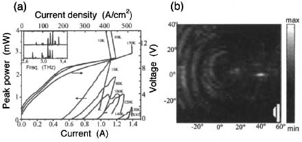
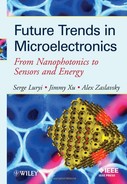
Figure 2. (a) Light and bias voltage vs. current of a four-quantum-well active region device measured a various temperatures, as indicated. The maximum operating temperature reached by this device is 150 K. Inset shows the spectrum of device measured for two different drive currents, (b) Far-field spectrum of the device: horizontal axis is the growth direction, vertical axis is in the plane of the device.
The light-current characteristics of the MBE-grown sample EV1136 is reported as a function of temperature in Fig. 2. The maximum temperature achieved in the device shown is 158 K.
3. Antenna-like third-order distributed feedback QCL
The problems with the devices based on metal-metal waveguides, like the one shown in Fig. 2, consist of both relatively low output power as well as a very broad far-field emission. These problems arise from the use of a metal-metal waveguide and they severely limit the usefulness of the device for applications. To try and alleviate these problems, we investigated a distributed feedback (DFB) grating15 resonant with the third-order Bragg condition.
In our approach, in contrast to approaches based on surface emission,16 we optimize the natural edge emission of the TM-polarized light in the structure by utilizing a third-order DFB grating. This simultaneously provides the feedback for the optical mode inside the semiconductor and the necessary diffraction to couple the radiation out to free space. An intuitive picture of the system is given in Fig. 3(a): a waveguide mode with propagation constant β = neffk0 (black arrow) incident on an infinite length grating with periodicity Λ, is diffracted back by the reciprocal vectors G =2π/Λ (light arrows). In the case of a third-order grating G = 2β/3, and when the refractive index neff = 3, the first two diffractions match the wavevector of the mode propagating in the air in the horizontal direction, while the third one provides the feedback in the waveguide. The estimated effective refractive index for double metal waveguides is ~3.5, a value close to the relation neff = 3 that would allow the use of the grating to extract the light out of the semiconductor. Efficient coupling is nevertheless achieved because of the finite length of the large refractive index contrast grating.
The latter has been realized by deep dry etching of the semiconductor along the waveguide, alternating active region and air with a duty cycle of ~10%, as shown in Fig. 3(b). To avoid the parasitic higher-order lateral and longitudinal modes, we used the same geometry reported for the photonic crystal structures of reference:17 all around the waveguide we left an unmetallized region, in order to use the thin heavily-doped semiconductor lying on the top of the waveguide as an absorbing layer.
We designed the grating to overlap the gain frequency of our active medium with the mode on the left side of the gap, where the electromagnetic energy is more confined in the semiconductor region.

Figure 3. (a) Vector diagram for a third-order DFB in the wavevector space k. Arrows labeled with β represent modes propagating inside the semiconductor and arrows labeled with G represent the grating diffraction vectors. The upper half circle has a radius equal to the wavevector of the mode propagating in the air k0, so it represents the light cone: vectors ending on the circle can couple out of the semiconductor. (b) Schematic drawing of the active region sandwiched in the metal-metal waveguide with the deep-etched third-order grating.
Figure 4. (a) Normalized emission spectra of the third-order DFB for different grating periods Λ. Inset: spectrum in logarithmic scale. (b) Far-field of the emitted spectrum. The optical power reaches 14 mW in pulsed mode.
For all the devices we measured the light–current–voltage (L–I–V) curves in pulsed mode at 10 K and the emission spectra for different operating currents with a resolution of 0.1 cm–1. The output peak power measured for a typical DFB device was 15 mW, a factor of 7 higher than for a standard double-metal waveguide of similar dimensions. The slope efficiency was also improved, reaching the value of 130 mW/A, considerably higher than the highest value of 40 mW/A shown for surface emitting structures.16,18 This is due to the combined effects of improved extraction and collection efficiency.All the devices worked in single mode operation with 30 dB sideband suppression ratio; their emission frequency can be tuned over 0.17 THz by changing the grating period – see Fig. 4(a). These two results, the enhancement of the output power and of the slope efficiency, already prove the simple model given above of the grating as means to outcouple single mode laser light from a double metal waveguide. Moreover, the laser performance of our structure has another important advantage: the reshaping of the emission pattern in to a single lobed beam. To understand the effect of the grating, we can turn to the well-known concept of a linear phased array in antenna theory: the periodic apertures define a series of sources phase-shifted by π along the waveguide. Constructive interference from the different emitters can then be observed only in a narrow spot emitted in the direction along the array.
A systematic characterization of the far-field laser beam pattern has been carried out on the devices. The results are presented on two-dimensional graphs where the α and β axes correspond respectively to angular scans in the planes perpendicular to and parallel to the grating slits: point (0°, 0°) corresponds to a longitudinal edge emission, whereas point (90°, 0°) corresponds to surface emission. Data were acquired over a range of 150° along the horizontal direction, but for more clarity we show a magnification in the region where the beam is observable.
In Fig. 4(b) we show the measured far field for a typical DFB structure: the laser light in emitted in a single-lobed narrow beam of ~10° of divergence. We show the control of the laser emission wavelength and the enhancement of the output power due to the improvement in extraction efficiency. Moreover, we show that the grating can act as an array of phased linear sources, reshaping the typical wide and patterned far field of double-metal waveguides into a narrow beam of ~10° divergence in both directions.
4. Circuit-based QCLs
In a number of applications, it would be desirable to have lasers with a very small active volume. Dielectric-based resonators are fundamentally limited to a volume of the order of (λ/n)3. In contrast, metallic-based cavities do not suffer from the same kind of limitations. In fact, resonant inductance capacitor (LC) circuits can confine the electric field in an almost arbitrarily small volume. We investigate such cavities in which the dielectric of the capacitor is replaced by a QCL material.
Besides the small volume, another interesting property of such cavities is that they are inherently single-mode, with a well-behaved far field. Control of the emission frequency is trivial and can be achieved by merely changing the value of capacitance or inductance. Because of their small size and the fact that their frequency can easily be set, such devices lend themselves easily to the fabrication of arrays that could cover a wide spectral band. The radiative Q of such cavity will grow as λ3/V, i.e. the quality factor will increase as the volume V decreases. As noted by many recent theoretical contributions, the characteristics of such a “small laser” would depart significantly from the predictions of semi-classical theory and exhibit new features not observable in conventional structures.19
An attractive feature of QCL materials is the wide bandwidth of the gain material. The use of such bandwidth has been a challenging task in the THz regime, as coupling from the metal-metal waveguides into free space where the wavelength filter is located is difficult because of the geometrical and impedance mismatch between the optical mode and free space. The use of an LC circuit would enable an easy coupling to tuning elements, being either inductive or capacitive.
As discussed in the introduction, there is a strong interest in the physics community to study the strong coupling between a cavity and a quantum system. Such studies have already been carried out in the electronic domain at GHz frequencies by using Josephson junctions coupled to superconductive stripline resonators.14 Clearly, the LC circuit is a very interesting object in this context because it does not exhibit any clear size scaling limit other than the thickness of the quantum object it is coupled to. In fact, the area of the capacitor can be continuously scaled down as the thickness is reduced, and the limit to the value of L is only the radiative losses. Moreover, the radiative Q increases with decreasing circuit size, as shown by two classic antenna studies.20,21 For quantum optics experiments, Ohmic losses could be quenched by the use of superconductors assuming one operates at a sufficiently low frequency ν < 1 THz.
The spontaneous emission mid-infrared and THz radiation by solid state sources, and in particular by quantum cascade structures, is extremely inefficient because of both the low radiative efficiency of the transition as well as the poor extraction efficiency of high refractive index structures. In an LC resonator, the radiative Q can be decreased by a suitable choice of the size of the inductor, and the spontaneous emission can be increased by the Purcell effect. The Purcell factor, measuring the enhancement of the spontaneous emission rate in a cavity with a quality factor Q and a volume V is written as:
![]()
Because the volume of the cavity can be driven orders of magnitudes below λ3, the Purcell factor could in principle be 103–104 in a structure designed for this purpose. As a result, efficient room-temperature emission could be achieved as the quantum efficiency could be increased to values close to 10–2–10–3, depending on the wavelength. We believe this approach has many advantages compared to other attempts in this direction that use metallic optical cavities.22
We have carried preliminary experiment that demonstrates the feasibility of such a structure. Figure 5 shows a scanning electron micrograph of a possible LC resonator consisting of a symmetric arrangement of two capacitors connected by a section of straight wire. The capacitors consist of two metallic planes on each side of a quantum cascade active region designed to operate at the frequency of 1.5–1.6 THz. Electromagnetic finite element simulations of the structure predict a resonant frequency of the structure at 1.52 THz.

Figure 5. (a) Schematic of diagram of an LC resonator; (b) SEM micrograph of an LC circuit designed to operate in the THz – overall length of the resonator is 35 μm, much shorter than the wavelength in vacuum (200 μm).

Figure 6. (a) Narrowing of the emission spectrum and (b) light intensity vs. current for an LC resonator operating at 10 K. Strong oscillation is achieved.
Another structure based on the same concept was operated at cryogenic temperatures and driven by a small continuous current of 1.5 mA. Figure 6 shows the L–I curve as well as a spectrum of the device. From the exponential growth of the optical power with current as well as from the narrow emission spectrum, it is clear that self-sustained oscillation has been achieved in the THz by using the coupling between a quantum solid state system and a classical LC resonator of deep subwavelength dimension.
5. Conclusions
Since they are based on semiconductor processing techniques, THz QCLs have an excellent potential for the development of new sources in the 1–10 THz frequency range. We have shown that microwave-inspired resonators can lead to devices with very attractive features. A third-order distributed feedback QCL demonstrated single-mode operation, narrow far-field emission, and a high output power. We have also demonstrated the operation of a circuit based on an LC circuit where the gain is provided by QCL active material.
Acknowledgments
This work was supported by the Swiss National Foundation under the NCCR Quantum Photonics project.
References
1. P. H. Siegel, “Terahertz technology,” IEEE Trans. Microwave Theory 50, 910 (2002).
2. M. Tonouchi, “Cutting-edge terahertz technology,” Nature Photonics 1, 97 (2007).
3. P. Haring Bolívar, M. Nagel, F. Richter, M. Brucherseifer, H. Kurz, A. Bosserhoff, and R. Büttner, “Label-free THz sensing of genetic sequences: Towards ‘THz biochips’,” Phil. Trans. Royal Soc. A 362, 323 (2004).
4. M. Belkin, F. Capasso, F. Xie, A. Belyanin, M. Fischer, A. Wittmann, and J. Faist, “Room temperature terahertz quantum cascade laser source based on intracavity difference-frequency generation,” Appl. Phys. Lett. 92, 201101 (2008).
5. J. Faist, F. Capasso, D. L. Sivco, C. Sirtori, A. L. Hutchinson, and A. Y. Cho, “Quantum cascade laser,” Science 264, 553 (1994).
6. M. Beck, D. Hofstetter, T. Aellen, et al., “Continuous wave operation of a mid-infrared semiconductor laser at room temperature,” Science 295, 301 (2002).
7. R. Köhler, A. Tredicucci, F. Beltram, et al., “Terahertz semiconductor-hetero-structure laser,” Nature 417, 156 (2002).
8. L. Ajili, G. Scalari, D. Hofstetter, et al., “Continuous-wave operation of far-infrared quantum cascade lasers,” Electronics Lett. 38, pp. 1675 (2002).
9. G. Scalari, L. Ajili, J. Faist, H. Beere, Ε. Linfïeld, D. Ritchie, and G. Davies, “Far-infrared (λ ~ 87 μm) bound-to-continuum quantum-cascade lasers operating up to 90 K,” Appl. Phys. Lett. 82, 3165 (2003).
10. B. S. Williams, S. Kumar, Q. Hu, and J. L. Reno, “Operation of terahertz quantum-cascade lasers at 164 K in pulsed mode and at 117 K in continuous-wave mode,” Opt. Express 13, 3331 (2005).
11. S. Kumar, Q. Hu, and J. Reno, “186 K operation of terahertz quantum-cascade lasers based on a diagonal design,” Appl. Phys. Lett. 94, 131105 (2009).
12. C Walther, G. Scalari, J. Faist, H. Beere, and D. Ritchie, “Low frequency terahertz quantum cascade laser operating from 1.6 to 1.8 THz,” Appl. Phys. Lett. 89, 231121(2006).
13. C. Walther, M. Fischer, G. Scalari, R. Terazzi, N. Hoyler, and J. Faist, “Quantum cascade lasers operating from 1.2 to 1.6 THz,” Appl. Phys. Lett. 91, 131122(2007).
14. G. Scalari, N. Hoyler, M. Giovannini, and J. Faist, “Terahertz bound-to-continuum quantum-cascade lasers based on optical-phonon scattering extraction,” Appl. Phys. Lett. 86, 181101 (2005).
15. L. Mahler, R. Kohler, A. Tredicucci, et al., “Single-mode operation of terahertz quantum cascade lasers with distributed feedback resonators,” Appl. Phys. Lett. 84, 5446 (2004).
16. S. Kumar, B. Williams, Q. Qin, A. W. M. Lee, Q. Hu, and J. Reno, “Surface-emitting distributed feedback terahertz quantum-cascade lasers in metal-metal waveguides,” Opt. Express 15, 113 (2007).
17. Y. Chassagneux, R. Colombelli, W. Maineult, et al., “Electrically pumped photonic-crystal terahertz lasers controlled by boundary conditions,” Nature 457, 174(2009).
18. J. A. Fan, M. Belkin, F. Capasso, S. Khanna, M. Lachab, A. G. Davies, and E. H. Linfield, “Surface emitting terahertz quantum cascade laser with a double-metal waveguide,” Opt. Express 14, 11672 (2006).
19. K. Roy-Choudhury, S. Haas, and A. F. J. Levi, “Quantum fluctuations in small lasers,” Phys. Rev. Lett. 102, 053902 (2009).
20. L. J. Chu, “Physical limitations of small antennas,” J. Appl. Phys. 19, 1163 (1948).
21. H. A. Wheeler, “Small antennas,” IEEE Trans. Antenn. Propag. 23, 462 (1975).
22. Y. Todorov, I. Sagnes, I. Abram, and C. Minot, “Purcell enhancement of spontaneous emission from quantum cascades inside mirror-grating metal cavities at THz frequencies,” Phys. Rev. Lett. 99, 223603 (2007).