Device Proposals Beyond Silicon CMOS
IBM, SRDC, T.J. Watson Research Center Yorktown Heights, NY 10598, U.S.A.
1. Introduction
As the end of the silicon evolutionary path nears, alternative devices are being proposed on an urgent basis. Such devices involve different materials such as carbon, III-V semiconductors, etc., different geometries, such as nanotubes, nanowires and graphenoid sheets, and different operating principles involving collective phenomena such as coherent tunneling and ferroelectricity and density of states engineering for band-to-band tunneling FETs. All add to a weird device menagerie that needs some sorting out. These device proposals are mostly not new, but they are enabled by the march of technology and the apparent need for a device that breaks the inflexible switching-energy vs. performance limit of silicon CMOS technology. Meanwhile the goalposts shift continually with the evolution of CMOS technology and system design. Here I will attempt to describe and evaluate the most promising to the most outlandish of these devices in terms of future needs for large scale computation.
2. Industry view
End of CMOS scenarios and successor technologies to CMOS have been the fascination of the semiconductor industry for at least the past decade. Numerous project initiatives and focus centers have provided support into research on alternative devices, circuits and architectures, most notably as part of the Semiconductor Research Corporation’s (www.src.org) Nanoelectronics Research Initiative (NRI) and Focus Center Research Program (FCRP). So far the lack of success has been notable except perhaps for the RSFQ logic family,1 an ultra-high speed superconducting technology operating at cryogenic temperatures. This logic family has been dropped from the ITRS (2007) menu because working prototypes had been demonstrated but the market had not materialized. The industry view is encapsulated in the chart2 reproduced in Fig. 1 with the “state variable” shown at the bottom and proceeding to increasingly higher levels of implementation toward the top (although a strictly 1:1 progression is not implied). A primary motivation exemplified by this chart is to replace charge with some other variable (polarization, spin, phase, etc.), and the rationale is that a non-charge based state variable may lead to a smaller switching energy since it avoids the electrostatic energy associated with charging the gate capacitance of an FET. Thus we see spintronics features quite prominently in the research efforts as well as propagation of electric or magnetic polarization in quantum cellular automata (QCA) type of effects.
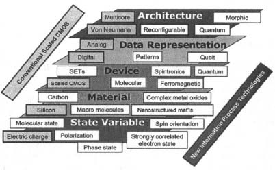
Figure 1. Chart from 2007 International Technology Roadmap, Emerging Research Devices2 showing the emphasis on other state variables besides charge for the new information process technologies. [Reproduced by permission from the Semiconductory Industry Association, International SEMATECH: Austin, TX (2007)].

Figure 2. Quantum cellular automaton (QCA) principle, after Lent:3 (a) clock-driven polarization wave propagation along a chain of QCA gates; (b) majority logic gate where the bottom two inputs determine the output state.
Setting aside quantum computation, which is really in a class by itself and will not be discussed here, the proposed solutions fit rather poorly into Von Neumann type architectures, thus research into compatible architectures is integral to assessing the place of some of the more exotic proposals. Much excellent work has been done in exploring these various avenues, and many significant advances have been made, some of which will be discussed below. Still, so far it seems that the further one strays from the CMOS path (left edge of the chart) the less viable the proposals seem to be. Why is it that CMOS seems to have such an unbreakable monopoly?
While competitors so far have been unable to assault the well-nigh impregnable CMOS fortress, CMOS and silicon technology is changing in ways that perhaps can give potential competitors a foothold. With silicon nearing the end of its scaling potential, many new solutions are being tried involving an expanding materials inventory. Silicon itself, apart from its role of supporting substrate, is only one layer among many for silicon-on-insulator realizations. Novel self-assembly and hybrid three-dimensional (3D) integration schemes allow the incorporation of other technologies into the silicon mix. Thus the path towards incorporating a novel logic or memory technology is becoming easier.
3. Other state variables
Computational state variables are simply the physical attributes of a system that carry computational information. The motivation to replace the presently used state variable (voltage, misleadingly called charge) is that the bulk of the energy to switch states (voltages) is used to charge circuit nodes comprising of internal device capacitances, parasitic inter-electrode capacitances and interconnects. Note that the logic is propagated electromagnetically from circuit to circuit at speeds approaching the speed of light. It is the nonlocal character of the voltage distribution that costs so much in terms of electrostatic energy. Nanoscale CMOS at the 22 nm node of the ITRS Roadmap has internal switching energies of ~10-18 J for a minimum sized device but ~10-16 J when including interconnects.
There is some confusion, as evidenced in Fig. 1, between the above definition and the use of “state variable”, such as charge, to describe the internal state of a logic-switching device. In conventional devices this relationship is not one-to-one, since the internal charge is a function of device size, circuit design, etc. An abrupt change of state is desired, controlled by a small change of the terminal voltages, which is why collective and strongly correlated states are being sought in new devices.
When an internal state variable is used to directly represent digital bits, it is called a token. Information processing occurs by physically passing the token from device to device. This system is attractive because of the isomorphism between the state variable and the logic state heralds perhaps a greater energy efficiency compared to the conventional approach and perhaps a more robust representation compared to the arbitrary nature of voltage representation.
The token-carrying logic is exemplified by the QCA3 approach, as shown in Fig. 2 where the states are represented by two diagonal alignments of internal polarization. The states are separated in energy by several kT, yet transitions can be propagated from cell-to-cell by means of a traveling wave generated by external clock electrodes that adiabatically facilitate the dipole rotation by compensating for the internal potential so that the cell polarization may be driven by weak neighboring fields. An instructive example was recently given for a magnetic QCA.4,5 Calculations of energy dissipation for adiabatic transitions (slowly variable field) for flipping of electric and magnetic polarizations3,4 and spins6 show that it may be very small, much less than kT. Thus far, efforts in the field of token-passing logic have focused naturally on demonstrations of proof of concept, some with notable success3 but a set of more fundamental questions remain.
Compared to electromagnetic propagation, the speed of propagation of the tokens is much smaller, typically by a factor of ~103. Also, logic interactions are predominantly via neighboring cells (cellular automaton). This gives rise to the following set of questions which to date have not been satisfactorily addressed: (i) cellular automata have inherent limitations and inefficiencies in implementing general purpose logic, which would result in some penalty factor vis-à-vis CMOS; (ii) many state transitions are utilized for communication rather than logic, which would result in further penalties; (iii) how does the communication penalty associated with token passing limit applications? (iv) the reactive power for such a system will be very large (creating the propagator fields) so that very high Q clock power supplies will be needed to maintain efficiency, but at present there are no solutions for this.
A family of proposed devices uses state variables other than charge to modulate their switching characteristics while still using external voltage and current for logic propagation. These include the Das-Datta spin transistor7,8 (see Fig. 3) where the gate modulates the spin lifetime, the Mott transition,9,10 quantum correlated states,11 quantum interference devices, etc. The device itself needs to be a two-way transducer, converting from the terminal voltages to the internal state variable and back again. The advantages of changing state variable, for instance a claimed lower operating voltage for the spin-transistor, have to offset losses in the transducer chain, and this has been difficult to achieve.

Figure 3. Spin transistor, after Datta and Das,7 with crossed polarizers on source and drain. Enhanced spin-orbit coupling due to the gate field promotes rapid injected spin thermalization and thence transmission of a portion into the drain.
4. Scaling
Capacitance scales inversely with distance and density with area, so that scaling capability has always been an important and desirable characteristic for all new device proposals. The electrostatic QCA, for instance, has the ability to scale all the way down to molecular dimensions. Scaling has, of course, been extensively discussed elsewhere, but here we will briefly touch on aspects of new devices which make them interesting from the scaling perspective. Even the more conventional technologies are exploring quantum-confined geometries such as nanowires and nanotubes. These confer scaling advantages as a result of reduced dimensionality much like those conferred on 1D quantum confined lasers. For instance, as illustrated in Fig. 4, 1D quantum confinement collapses the transverse density of states into a single quantum number (not counting degeneracy), so that the current-carrying capacity of the quantum channel is independent of device cross-section. Thus carbon nanotubes can be scaled below 1 nm diameter and are still capable of carrying twice (for band degeneracy) the full quantum of conductance 2e2/h times supply voltage worth of current, typically ~20 μΑ. Some shibboleths may fall by the wayside, such as the need for the gate to always be in close proximity to the channel of an FET. As illustrated in Fig. 5 it may be possible use highly polarizable materials to transmit potentials into small devices12 or even molecules,13 to control their switching. Another exciting possibility is to use collective effects to suppress single-electron tunneling and reduce lateral dimensions. Some work on oxide semiconductors, while still open to interpretation, has shown control of device properties on an extremely small scale.14
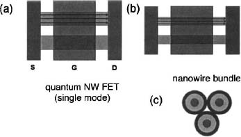
Figure 4. Nanowire scaling: shrinking width of nanowire (a) to (b) compresses the same amount of active charge into a smaller width therefore increasing the ratio of active to parasitic capacitance; (c) reduction of parasitic capacitance by nanowire bundling.

Figure 5. Field effect transistor with a very high-permittivity gate dielectric where the gate dielectric thickness may be much larger than the channel length, CIS and CID are the gate fringing capacitances to source and drain respectively.
5. Beating kT(/e)
At this point in the evolution of integrated computing the overwhelming concern is power reduction or, in terms of individual device properties, the energy stored or dissipated per switching event. With today’s numbers of transistors per chip at ~1 billion, total power constrained to below ~1 W and frequencies in excess of 1 GHz, average switching energies need to be below 10-17 J per transistor, and these demands will increase exponentially with time. As Table 1 shows, there is a distinction between switching energy kT and the energy per electron kT/e. The former places an absolute limit on the energy cost of nonreversible computation,15 while the latter places a restriction on power supply voltage as applied to electron-barrier controlled devices such as FETs. That is, for a given ION/IOFF current ratio r, a switching voltage V = kT(/e) In r is required. This is the famous “60 mV/decade” subthreshold slope problem, and much research effort, funded by a dedicated government program, is devoted to finding devices with steeper that 60mV/decade slopes. This voltage requirement, coupled with the fact that the capacitance per unit length of the interconnects is a constant ~1 times the permittivity of the dielectric, means that switching energy, 1/2 CV2 , is rather insensitive to technology changes16 depending only on the general length scale. To reduce switching energies therefore requires device, circuit and architectural innovation in addition to scaling. Here we will focus on device innovation. As discussed in a previous paper in this series17 carbon-nanotube FETs may enable improved switching energies compared to CMOS simply by virtue of their higher performance, therefore offering a better power-performance trade-off, but to go beyond this requires devices operating on different principles.
Table 1 lists various “workaround” solutions, both to the 60 mV/decade problem and also to the fundamental “kT limit”. The latter limit only applies to irreversible operations, i.e. all conventional computation, but the token-passing kind of logic including QCA with electric or magnetic dipoles, and spintronics generally postulate a reversible mode of computation where the clock is varied adiabatically and much of the energy can be recovered (notwithstanding the questions we posed earlier).
It should be noted that CMOS logic could, in principle, also be run in a reversible or partly reversible manner,18 but the technical obstacles to achieving significant energy savings are daunting.
The kT and kT/e limits may be circumvented simply by reducing temperature, and this approach has a long history,19 but in the end refrigerator inefficiencies and the Carnot factor have to be taken into account. Much has been made of the fact that electronic spin interacts weakly with the thermal bath and therefore may achieve lower energy dissipation.6 An illustrative scheme is shown in Fig. 6. Spin-polarized electrons are injected into a nonmagnetic semiconductor via a polarizer. In the semiconductor the spins may be flipped by weak fields involving voltages of ![]() kTle and may interact with each other to do logic. In reality what we have here is a refrigerator, since the injected spins have a super-cooled distribution in the zero-magnetic gap semiconductor.20 Logic can be performed as long as execution times are much shorter than the thermalization time, and the electrons may be extracted (read) via a similar polarizer at no energy cost. However any electrons where the spin has been flipped, either intentionally or through interaction with the thermal bath, will have to be extracted via a complementary polarizer, but to prevent back-injection of the opposite spin polarization and hence contamination of the distribution, this polarizer has to be biased at a voltage of several kT/e with respect to the original injector. From this it is clear that the Carnot penalty is paid back (at least) during this extraction process. It may be justifiably argued that this constitutes a very compact and efficient refrigerator, but remember that this scheme is incomplete since only one degree of freedom (spin) has been cooled this way.
kTle and may interact with each other to do logic. In reality what we have here is a refrigerator, since the injected spins have a super-cooled distribution in the zero-magnetic gap semiconductor.20 Logic can be performed as long as execution times are much shorter than the thermalization time, and the electrons may be extracted (read) via a similar polarizer at no energy cost. However any electrons where the spin has been flipped, either intentionally or through interaction with the thermal bath, will have to be extracted via a complementary polarizer, but to prevent back-injection of the opposite spin polarization and hence contamination of the distribution, this polarizer has to be biased at a voltage of several kT/e with respect to the original injector. From this it is clear that the Carnot penalty is paid back (at least) during this extraction process. It may be justifiably argued that this constitutes a very compact and efficient refrigerator, but remember that this scheme is incomplete since only one degree of freedom (spin) has been cooled this way.

Table 1. Physical constraints.

Figure 6. Device with spin polarizers for injection and readout. The spin transport medium has zero bandgap for spin-spin interactions. The readout electrodes have to be biased at a sufficient potential to prevent back injection.
Practically the kT/e limit is more important than the KT limit since voltage and interconnect capacitance place switching energies today above 104 kT and this places emphasis on strategies to increase the sharpness of the switching transition. Two such strategies, listed in Table 1, are energy filtering and collective effects. These will be dealt with in the following sections.
6. Energy filtering
The principle of energy filtering is outlined in a previous FTM book chapter21 and indeed can be traced back to the Esaki diode. The principle, as applied to an n-FET, is illustrated in Fig. 7. When the FET is in the “on” state, electrons originating in the valence band of the p-type source tunnel into the conduction-band of the channel. The device is turned off by raising the conduction-band edge in the channel above the valence band edge in the source. One can say that the Fermi tail of the electrons in the valence band has been cut off above the valence band edge permitting a steeper than 60mV/decade subthreshold slope. While the principle is clear, achieving a steep slope in practice has been difficult and so far has only been demonstrated unambiguously in a carbon nanotube geometry,22 and only at low currents, unsuitable for high-speed devices. Band-to-band tunneling transmission coefficients decrease exponentially with mr1/2 and EG3/2 where mr is the reduced effective mass for tunneling and EG is the band gap. Thus materials with small mr and EG are desired. A direct bandgap is also important to achieve large current levels. Materials such as carbon nanotubes, graphene ribbons,23 III-V semiconductors and Ge (with an almost direct bandgap) have the required properties.
Incorporation of heterojunctions,24 as shown in Fig. 7(b), can provide the correct band line-up for the desired tunneling while suppressing tunneling where it is not wanted, such as from the drain into the channel. Nanowires (or nanotubes), with wrap-around gates, are the preferred geometry since this provides an intimate electrostatic control of the tunnel junction by the gate.
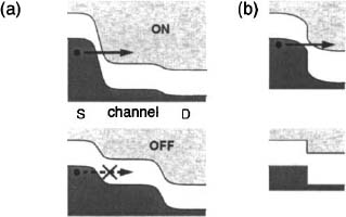
Figure 7. Operating principle of a tunnel field-effect transistor, after Appenzeller et al.:2 (a) the bands are crossed in the “on” state and uncrossed by the gate voltage in the “off” state; (b) a staggered gap heterojunction achieves a smaller bandgap for tunneling while allowing a larger bandgap in the source and channel regions.
7. Band structure engineering
While conventional device design has assumed the band structure as a given (e.g. bulk silicon), quantum effects on the nanoscale can alter band energies. This may be exploited, in the case of graphene, to make nanoribbons with controlled bandgaps as in proposals for the tunnel FET.23 For graphene nanoribbons of a certain type the dispersion of edge states (see Fig. 8) may be controlled by a lateral field and this dispersion-modulation has been proposed as a new way of modulating the current,25 since transport can occur only when there is finite dispersion. Similarly, other proposals exploit the ability of a perpendicular field to modulate the bandgap of bilayer graphene.26
8. Collective effects
Going back to Table 1, the kT/e potential can simply be replaced by kT/ne where n is much larger than unity. In other words, collections of correlated particles still have mean thermal energies of ~kT but a much lower electric potential than kT/e (as seen in Table 1, increased n also offers potential scaling benefits since it reduces h/p). Collective effects are being evoked to extend devices beyond ultimate CMOS, where dimensions are on the 10 nm scale. A legitimate question therefore is how do the collective effects withstand scaling where n decreases perhaps as fast as the cube of the dimension. In the case of ferromagnetism, experiments and theory indicate that scaling down to ~5nm is possible,27 and experiments on semiconducting oxides14 show effects persisting on the ~2 nm distance scale.

Figure 8. Bandwidth modulation FET, after Raza:25 (a) lateral gate applied to a graphene nanoribbon; (b) gate field breaks the symmetry and adduces a finite bandwidth to the midgap edge states.
This can be exploited in switching ferromagnetic of ferroelectric domains, in the Mott metal-insulator transition, in correlated electron condensations such as bi-layer graphene28 or semiconducting oxides29 and in correlated tunneling. In addition to the number effect, there are also quantum exchange interactions that reduce potential energies and can give rise to a “negative capacitance”,30 and by inference to switching behavior. As is seen from the above list, the field is rich and just beginning to be explored. Here we will cite just two examples of current research interest.
Ferroelectricity leads to hysteretic charge vs. voltage characteristics (analogous to the well known hysteretic loops of ferromagnetism). This is being exploited commercially for memory applications and it has also been proposed for logic devices as a way of increasing the subthreshold slope.31 It is proposed that by combining the negative capacitance of an unstable ferroelectric state with the positive gate capacitance an FET, that the system may be made marginally stable with the internal gain resulting in an almost vertical off-on transition – see Fig. 9. The viability of this idea involves many questions concerning domain formation, gain per unit volume, speed, etc. Similar proposals are in place for a purely electronic negative capacitance resulting from strong quantum mechanical exchange effects,30 as have been seen in oxide semiconductors. Ferromagnetism itself may be used for logic as in the case of magnetic QCA. Also, ferromagnetic spin-wave logic32 is being explored. Research is also being done into multiferroics, especially composite coupled systems,33 where electric fields may control ferroelectric properties and vice versa.
The other example involves inducing correlated tunneling across two graphene layers28 separated by an insulator, as shown in Fig. 10. When the “nesting” condition is achieved and the electron and hole Fermi surfaces on the two sides are matched, correlated tunneling can occur and the resistance between the two layers is reduced from an insulator-like value to just the quantum of conductance. The remarkable prediction is that the conductance in the “on” state is just the quantum of conductance 2e2/h and does not depend on the insulator thickness, even though uncorrelated tunneling current is thus reduced exponentially. This state has not been experimentally confirmed, but a low-voltage device has been proposed by analogy to the superconducting Josephson junction.34

Figure 9. Ferroelectric element (a) in series with the gate of an FET; (b) the ferroelectric response (derivative of (a), highly idealized) is added to the response of the series gate capacitor CG designed to maximize the change in polarization following small changes in gate voltage. After Ref. 31.

Figure 10. Bilayer pseudo-spin FET, after Banerjee:34 (a) two graphene sheets separated by an insulator and gated on top and bottom; (b) bands of the two layers shifted by the gate-induced potential into the “nesting” condition where the electron and hole Fermi surfaces coincide (c), for correlated tunneling between the layers.
9. Outlook
In the above treatment we have tried to convey a flavor of the many approaches used and avenues being investigated to come up with a future device that is better, mainly in terms of power dissipation, than CMOS. Much has been left out and much worthy work left unmentioned, due to lack of space and lack of personal familiarity. For this I apologize. Most of the approaches have not yet resulted in working demonstrations, let alone CMOS-competitive ones. This does not in anyway diminish the quality and importance of this work, since truly a new frontier is being explored and only those in the future, looking back, will be able to evaluate the fruits of today’s efforts.
Acknowledgments
I wish to acknowledge the help of the following in the form of discussions and material supplied: Siyuranga Koswatta, Jeff Welser, and Steven Koester.
References
1. P. Bunyk, K. Likharev, and D. Zinoviev, “RSFQ technology: Physics and devices,” Intern. J. High Speed Electron. Syst. 11, 257 (2001).
2. 2007 International Technology Roadmap, Emerging Research Devices, www.itrs.net/Links/2007ITRS/2007_Chapters/2007_ERD.pdf
3. C. S. Lent and B. Isaksen, “Clocked molecular quantum-dot cellular automata,” IEEE Trans. Electron Dev. 50, 1890 (2003).
4. G. Csba, P. Lugli and W. Porod, “Power dissipation in nanomagnetic logic devices,” Digest 4th IEEE Conf. Nanotechnol. (2004), p. 346.
5. B. Behin-Aein, S. Salahuddin, and S. Datta, “Switching energy of ferro-magnetic logic bits,” IEEE Trans Nanotechnol. 8, 505 (2009).
6. D. E. Nikonov, G. I. Bourianoff, and P. A. Gargini, “Power dissipation in spintronics devices away from thermal equilibrium,” J. Supercond. Novel Magn. 19, 497 (2006).
7. S. Datta and B. Das, “Electronic analog of the electro-optic modulator,” Appl. Phys. Lett. 56, 665 (1990).
8. K. C. Hall and M. E. Flatté, “Performance of a spin-based insulated gate field effect transistor,” Appl. Phys. Lett. 88, 162503 (2006).
9. C. Zhou, D. M. Newns, J. A. Misewich, and P. C. Pattnaik, “A field-effect transistor based on the Mott transition in a molecular layer,” Appl. Phys. Lett. 70, 598 (1997).
10. C. Ko and S. Ramanathan, “Observation of electric field-assisted phase transition in thin film vanadium oxide in a metal-oxide-semiconductor device geometry,” Appl. Phys. Lett. 93, 252101 (2008).
11. S. Thiel, G. Hammerl, A. Schmehl, C. W. Schneider, J. Mannhart, “Tunable quasi-two-dimensional electron gases in oxide heterostructures,” Science 313, 1942 (2006).
12. W. Haensch, E.J.Nowak, R. H. Dennard, et al, “Silicon CMOS devices beyond scaling,” IBM J. Res. Develop. 50, 339 (2006).
13. N. D. Lang and P. M. Solomon, “Charge control in a model biphenyl molecular transistor,” Nano Lett. 5, 921 (2005).
14. C. Cen, S. Thiel, G. Hammerl, et al., “Nanoscale control of an interfacial metal-insulator transition at room temperature,” Nature Mater. 7, 295 (2008).
15. R. Landauer, “Irreversibility and heat generation in the computing process,” IBM J. Res. Develop. 3, 183 (1961).
16. P. M. Solomon, “Comparison of semiconductor devices for high-speed logic,” Proc. IEEE 70, 489 (1982).
17. P. M. Solomon, “Carbon-nanotube solutions for the post-CMOS-scaling world,” chapter in: S. Luryi, J. M. Xu, and A. Zaslavsky, eds., Future Trends in Microelectronics: Up the Nano Creek, New York: Wiley, 2007.
18. M. P. Frank, “Reversible computing and truly adiabatic circuits: The next great challenge for digital engineering,” 5th IEEE Dallas Circ. Syst. Workshop (DCAS-06), Richardson, TX, 2006.
19. R. H. Dennard, F. H. Gaensslen, H.-N. Yu, V. L. Rideout, E. Bassous, and A. Le Blanc, “Design of ion-implanted MOSFETs with small physical dimensions,” IEEE J. Sol. State Circ. 9, 256 (1974).
20. We are ignoring, for pedagogical purposes, the non-spin components of the electron’s energy, which, of course, still retain their original thermal distributions.
21. P. M. Solomon and C. R. Kagan, “Understanding molecular transistors,” chapter in: S. Luryi, J. M. Xu, and A. Zaslavsky, eds., Future Trends In Microelectronics: The Nano Millennium, New York: Wiley, 2004.
22. J. Appenzeller, Y.-M. Lin, J. Knoch, and Ph. Avouris, “Band-to-band tunneling in carbon nanotube field-effect transistors,” Phys. Rev. Lett. 93, 196805, (2004).
23. Q. Zhang, T. Fang, H. Xing, A. Seabaugh, and D. Jena, “Graphene nanoribbon tunnel transistors,” IEEE Electron. Dev. Lett. 29, 1344 (2008).
24. J. Knoch, M. T. Bjoerk, H. Riel, H. Schmid, M. Enderlein, H. Ghoneim and W. Riess, “Transport in heterostructure nanowire tunneling FETs,” 2nd Intern. Conf. One-Dimensional Nanomater., Malmö, 2007.
25. H. Raza, T. Ζ. Raza, T.-H. Hou, and E. C. Kan, “On the possibility of an electronic-structure modulation transistor,” arXiv:0812.0123v2 and v1 (2009).
26. G. Fiori and G. Iannaccone, “On the possibility of tunable-gap bilayer graphene FET,” IEEE Electron. Dev. Lett. 30, 261 (2009).
27. H. J. Richter, A. Y. Dob in, R. T. Lynch, et al, “Recording potential of bit-patterned media,” Appl. Phys. Lett. 88, 222512 (2006).
28. J.-J. Su and A. H. MacDonald, “How to make a bilayer exciton condensate flow,” Nature Phys. 4, 799 (2008).
29. S. Thiel, G. Hammed, A. Schmehl, C. W. Schneider, and J. Mannhart, “Tunable quasi-two-dimensional electron gases in oxide heterostructures,” Science 313, 1942(2006).
30. T. Kopp and J. Mannhart, “Calculation of the capacitances of conductors -Perspectives for the optimization of electronic devices,” J. Appl. Phys. 106, 1 (2009).
31. S. Salahuddin and S. Datta, “Use of negative capacitance to provide voltage amplification for low power nanoscale devices,” Nano Lett. 8, 405 (2008).
32. M. P. Kostylev, A. A. Serga, T. Schneider, B. Leven, and B. Hillebrands, “Spin-wave logical gates,” Appl Phys. Lett. 87, 153501 (2005).
33. Y.-H. Chu, L. W. Martin, M. B. Holcomb, et al., “Electric-field control of local ferromagnetism using a magnetoelectric multiferroic,” Nature Mater. 7, 478 (2008).
34. S. K. Banerjee, L. F. Register, E. Tutuc, D. Reddy, and A. H. MacDonald, “Bilayer pseudo-spin field-effect transistor (BiSFET): A proposed new logic device,” IEEE Electron. Dev. Lett. 30, 158 (2009).