GeOI as a Platform for Ultimate Devices
IMEP-LAHC/Minatec, Grenoble-INP, 3 parvis Louis Néel, Grenoble, France
CEA-LETI/Minatec, F38014, Grenoble, France
Div. of Engineering, Brown University, Providence, RI 02912, U.S.A.
1. Introduction
The International Roadmap for Semiconductors predicts increasing device and circuit performance through the reduction of the physical MOSFET gate length for years to come.1 At the same time, the supply voltage VDD will also continue to decrease, whereas the dynamic power consumption has to be limited to around 100 W/cm2 for the future Si technology nodes (< 45 nm). Hence, a strong enhancement of the transport properties is the key point for reliable future nodes. The on-state current ION of the MOSFETs is intrinsically linked and limited by the active semiconductor material, in particular for short-channel technologies where ballistic transport appears. Besides the incremental technological booster solutions for silicon CMOS (source-drain engineering, SOI, strained SOI, etc.), there is a strong research effort to conceive of new architectures, like the 3D stacking,2 or to replace silicon-based channels with higher mobility materials.
Germanium had been used decades ago to create the first generation of field effect and bipolar transistors. Unfortunately, the poor quality of its native oxide (GeO2) made it unsuitable for VLSI. However, the recent development of high-κ dielectrics and metal gates has rekindled interest in Ge as a promising candidate to replace Si for advanced CMOS technologies.3 The main advantages of Ge are: enhanced transport properties, especially for holes; a better match between electron and hole mobilities; and an excellent lattice match with GaAs (suitable for Ge and GaAs co-integration). The lower bandgap of Ge, while deleterious for leakage currents in standard MOSFETs, may also prove advantageous for advanced devices. Similarly to SOI, the germanium-on-insulator (GeOI) platform is beneficial for Ge MOSFET development through the improvement of the electrostatic control (essential for nanometric technologies) and the reduction of the Ge material consumption.4,5
Recently, high-performance 65 nm Ge PMOS devices with pockets, halos and NiGe metal source/drain metallization have been demonstrated: very good ION = 478 μΑ/μm and low IOFF = 0.9 μΑ/μm were achieved.6 The corresponding NMOS devices, on the other hand, have been less impressive. It is speculated that both the poor NMOS performance and the undesirable positive threshold voltage VT shift in Ge PMOS arise from the presence of unpassivated dangling-bond (DB) states located close to valence band edge,7,8 or from negatively charged interstitial hydrogen H-.9 Recently, alternative gate dielectrics technologies, such as GeO2 pre-gate passivation with HfO2 followed by fluorine post-gate treatment,10 and GeO2/Al2O3 stacking,” have shown promise of improving on standard SiOx/HfO2 approaches. If the Ge gate insulator passivation issue is resolved, GeOI will have a realistic prospect of mainstream technological insertion.
In this chapter, we review the recent progress on GeOI substrate manufacturing using both principal fabrication techniques, Smart-Cut™ and Ge enrichment, as well as variants like strained GeOI, Si-Ge co-integration, etc. We then discuss GeOI material characterization by the pseudo-MOS (Ψ-MOS) technique. The chapter concludes with a discussion of GeOI as platform for high-performance PMOS, as well as alternative devices, such as tunneling FETs (TFETs) and nanowires.
2. GeOI substrate engineering: Smart-Cut™ and Ge enrichment
The Smart-Cut™ technology can be applied to fabricate GeOI substrates. The Ge donor wafers can either be bulk substrates,12 or Si substrates capped with epitaxial Ge.13 The process sequence is illustrated in Fig. 1(a). After cleaning and chemical vapor oxide deposition (at 400 °C), Ge donor substrates are implanted with hydrogen (a few 1015/cm2 at 50-100 keV) and prepared for hydrophilic bonding onto a silicon base wafer at room temperature. After subsequent thermal processing, the bonded pair splits, producing a GeOI substrate and a Ge donor wafer that can be reused. Finally, polishing and annealing steps complete the fabrication of the GeOI substrate, delivering a smooth Ge film – see Fig. 1(b).

Figure 1. (a) Process sequence for the fabrication of GeOI via the Smart-Cut™ technology. Donor substrate A can be bulk Ge or epitaxially grown Ge. Substrate B is a Si handle wafer; (b) HR-TEM cross-section of the final GeOI substrate.

Figure 2. GeOI fabrication process by Ge condensation via oxidation: (a) SiGe layer is grown epitaxially on an SOI wafer; (b) oxidation of SGOI; (c) Ge is completely condensed and the top oxide is removed.
Depending on the Ge donor substrate nature and on the Ge/oxide interface, several GeOI substrate variants can be produced, like GeOxNy interface or compressively strained Ge layer on insulator.
The Ge enrichment (also called condensation) technique consists of germanium enrichment of a SiGe layer during oxidation. The first step of the condensation technique, illustrated in Fig. 2, is based on the growth of a pseudomorphic SiGe layer (i.e. strained layer below the critical thickness hC for plastic relaxation) on a SOI substrate. The resulting substrate is then oxidized at high temperature, as in Fig. 2(b). Silicon is oxidized preferentially, while the Ge diffuses through the SiGe layer to the buried oxide. If this process is continued, at some point Si is completely oxidized and the GeOI substrate can be obtained by removing the top SiO2 layer.
In the case of Ge condensation technique, SOI wafers are only used as substrates for the Si1-xGex layers that are subsequently Ge enriched. Since SOI wafers with thick top Si layers result in more Si atoms in the overall Si1-xGex/Si stack, the Ge enrichment process becomes more time-consuming. This problem can be alleviated by SOI thinning prior Si1-xGex epitaxial growth, with the target for the final top Si thickness being ~20 nm. In order to avoid defect generation, the grown Si1-xGex layer must remain below hc, which depends on the Ge content x, as shown in Fig. 3.14 An additional Si cap layer on the Si1-xGex layer can be used to prevent Ge consumption during the oxidation15 and thereby optimize the Ge enrichment.
To favor Ge diffusion and get continuous homogeneous Ge profiles within the silicon-germanium-on-insulator (SGOI) layers, periodic N2 annealing steps are added all along the process at 1050 and 900 °C.16 Figure 3(b) shows high-resolution cross-sectional TEM images of GeOI substrates obtained by Ge enrichment. Neither dislocations, nor stacking faults are seen on the TEM pictures. The Ge film thickness is around 10 nm and may subsequently be increased, e.g. by Ge epitaxy, for CMOS processing.17

Figure 3. (a) Critical thickness of plastic relaxation of SiGe layer grown epitaxially on Si as a function of the Ge content (dashed region shows metastable films, after Ref. 14); (b) cross-sectional TEM images of 10 nm thick Ge film on the GeOI wafer obtained by Ge enrichment.
3. GeOI material characterization: Ψ-MOSFET
In a world of constant evolution, SOI substrate development needs powerful tools to quickly and accurately characterize the raw material (before CMOS processing). Since a thin Ge film is fully depleted, the Ψ-MOSFET represents the accurate technique to scan the back-interface Ge/buried oxide (BOX) properties and to give crucial data on SOI and GeOI structure quality.5 The Ge film represents the body of the transistor and the BOX serves as the gate insulator. Two pressure-adjustable metallic probes act as drain and source. A backgate bias VBG induces accumulation or inversion at the BOX-film interface, as shown in Fig. 4(a). The ID(V8>BG) characteristics permit the extraction of the low-field mobility μ0, threshold voltage νT, subthreshold swing, interface state density Dit, etc. These extractions are carried out using the Y-function method,18 defined and illustrated in Fig. 4(b). The low-field mobility is calculated from the slope of the linear region of the characteristic, while the intercept of this tangent with the X-axis provides VT or flat-band voltage VFB. For thin films (< 100 nm), the potential of the front interface (passivated or not) modifies the back-interface potential through the effective electric field present in the film.19
The Smart-Cut™ technique is very attractive for BOX engineering and Ge/BOX interface passivation. Indeed, BOX nature can significantly affect the electrical properties like hole and electron mobility, as well as VT and VFB. Several Ge/BOX interface passivations have been investigated, particularly silicidation and nitridation via inductively-coupled plasma (ICP) treatments.
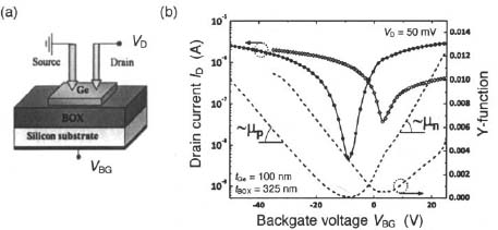
Figure 4. (a) Typical Ψ-MOSFET configuration on GeOI; (b) associated /D(VBG) curves for two GeOI structures. Parameters extraction is performed by the Y-function (= /D/gm1/2) method.18
An example of ICP nitridation leading to a 2 nm GeOxNy capping layer at the Ge/BOX interface is shown in Fig. 5(a). Very high electron mobility of ~675 cm2 /V·s is achieved, while hole mobility is maintained around 100 cm 2/V·s.20 Thus, the GeOxNy layer provides high electron currents, giving a possible passivation method for nMOSFETs on Ge or GeOI. The silicon passivation highlights the possibility of 2D Si-capping layer growth on Ge,21 as well as very good hole mobility improvement at the Ge/BOX interface. Recently, compressively strained Smart-Cut™ GeOI has been demonstrated, improving the hole mobility extracted by Ψ-MOSFET by over 30% (μp = 250 cm2/Vs for a 40 nm thick Ge film).22
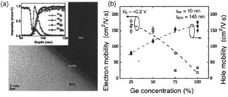
Figure 5. (a) HR-TEM cross-section of the GeOxNy capping leading to very high electron and hole back-channel currents (inset shows atomic species found at the back interface);20 (b) electron/hole low-field mobility extracted by the Y-function on enriched GeOI samples vs. Ge content.23
The Ge enrichment technique makes it possible to tune the Ge content in the SixGe1-x layer, to favor either electron or hole transport properties. Increasing the Ge concentration leads to a diminution of the electron mobility while the hole mobility is enhanced, as shown in Fig. 5(b).23 In addition, Ge enrichment provides the possibility of straining the epitaxial Ge layer, improving the hole transport properties still further, e.g. μp = 500 cmW·s.
To summarize, both methods of fabricating GeOI substrates have their own advantages and drawbacks. The Smart-Cut™ technique favors the possibility of tuning the back interface with various capping layers, providing high electron mobility substrates, whereas the Ge enrichment technique is more focused on the 2D co-integration and compressively strained substrates. A short overview of the present substrate performances is summarized in Fig. 6,24 where hole νS. electron mobility is plotted to illustrate the results of both methods.
4. High-performance pMOSFETs on GeOI: Achievements and challenges
• GeOI pMOSFET processing and performance
Once GeOI substrates are produced as described in the preceding section, pMOS devices can be fabricated using a somewhat modified CMOS process. After Ge stripping for mesa isolation,25 an additional Ge n-type doping via As implantation can be added to prevent front- and back-channel leakage, as well as the threshold voltage shift towards positive gate voltage.8,26 A ~1 nm Si capping is then deposited on Ge surface prior to the gate stack formation and oxidized to obtain a SiOx cap over Ge. With the silicon capping approach, it is possible to take advantage of the Si CMOS gate stack, since in this case HfO2 is deposited on Si/SiO2. 27 A 4–6 nm thick HfO2 gate oxide is formed by atomic layer deposition. The resulting EOT values vary around 2 nm with low gate leakage (IOFF = 0.6 μΑ/μm at (VG – VT) = –VD/3).27 This is followed by 10 nm TiN physical vapor deposition (PVD) and 50 nm Si n+-poly shunts. After DUV photolithography and gate etching, HfO2 is removed and BF2 S/D extensions are implanted and annealed, followed by HDD implantation (dose = 1015 cm-2, activated at 600 °C). The HDD implantation step is critical for GeOI pMOS, because n-dopants in Ge diffuse quickly28 and p-dopants do not29 (the converse is true in Si).
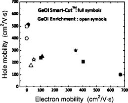
Figure 6. Hole vs. electron mobility extracted by Ψ-MOSFET for various GeOI samples (Smart-Cut™ and enriched GeOI). Reproduced from Ref. 24.
We fabricated pMOSFET devices on 200mm GeOI obtained both by Smart-Cut™ (Fig. 7)30 and by the Ge enrichment technique8,31 in a fully silicon-compatible process, demonstrating the first LG = 70 nm FD GeOI pMOS in 2008.26 The electrical characteristics of these transistors are shown in Fig. 8(a). We find that at VBG = 0 the back channel is turned on and that IOFF can be significantly reduced by biasing the backgate to VBG = 60 V. This effect has been seen in pMOSFETs made on GeOI obtained both by Smart-Cut™8,30,32 and Ge enrichment.31,33 The exact origin of this effect is uncertain, but interfacial states at the Ge/BOX interface could be responsible,7,8,31 as already observed in SOI.34

Figure 7. TEM image of 70nm gate length GeOI pMOSFET and HR TEM image of the corresponding Si/SiOx/HfO2/TiN gate stack.26

Figure 8. (a) Impact of n-type counterdoping of the Ge film on GeOI pMOSFET /D(VG) characteristics in linear regime (W= 10 μm, LG = 9 μm, VBG = 0 or 60 V); (b) impact of pockets on /D(VG) characteristics of LG = 70 nm gate GeOI pMOSFET at VBG = 0 (with n-counterdoping).
Since the fabrication of 200 mm GeOI wafers is only beginning, the quality of these substrates is not yet comparable to state-of-the-art SOI. As a result, temporary solutions such as channel n-type doping can be used to benchmark GeOI CMOS. The efficiency of channel doping is shown in Fig. 8, indicating that the parasitic conduction can be suppressed, making large V8>BG unnecessary. Likewise, the efficiency of pockets for very aggressive gate length (LG = 70 nm) devices is shown in Fig. 8(b).
For short-channel devices, the drain current is directly impacted by access resistance, which were extracted using Y-function method: RACC = Rs + RD ≈ 870 Ω μm. This value can be reduced by using germanide (e.g. NiGe) on S/D areas. By TCAD simulations we determined the expected ION improvement for the shortest LG = 70 nm device: +28% at VD = -1.2 V with RACC = 200 Ω·μm.26 Also, ION is affected by the carrier mobility, which we measured as 110 (80) cm2/V·s for long (short) devices - lower than the 250 cm2/V·s in undoped GeOI devices, but still better than undoped FD SOI pMOS.35 Low-temperature measurements, down to T = 77 K, show a saturation of the low-field mobility, highlighting a high density of defects along the channel. The temperature dependence of the low-field mobility and ION are well correlated. Hence, we expect a significant improvement of the mobility, and consequently ION, once the interface defect problem is solved and channel counterdoping is no longer needed.
The linear IOFF is reduced at low temperature, reflecting the SRH process reduction. As VD is increased, a high drain leakage appears in the accumulation regime, leading to IOFF current degradation. This leakage is partially suppressed at low T, as expected for a combination of trap-assisted tunneling (lowered at low T) and band-to-band tunneling (BTBT, independent of T).26 Reducing the trap density is expected to improve IOFF by a decade, but to go further the BTBT component must be minimized, which is a challenge because of Ge’s small bandgap. A way to reduce the BTBT is to operate at lower VD: Fig. 9 shows how IOFF is halved when VD is reduced from –1.2 to –1 V. More generally, Fig. 9 summarizes the measured and simulated ION/IOFF trade-offs for Ge and GeOI pMOSFETs.36,37,38 Simulations show that the addition of a germanide on S/D of short-channel LG = 70 nm pMOSFETs should enable a ION= 450 μΑ/μm at IOFF = 100 nA/μm (VD= –1 V).
Interestingly, a different GeOI approach has recently been reported with ultrathin (3 nm) Ge layer on SOI.39 This approach counts on quantum confinement in the Ge layer, which increases the effective band gap value and reduces the IOFF current while maintaining a negative VT without resorting to channel doping.

Figure 9. /OFF VS. /ON trade-off for GeOI pMOSFETs (LG = 120 and 70 nm), comparison with bulk Ge reference devices and TCAD simulations.
• Towards Ge based CMOS?
In parallel with pMOSFETs, we have fabricated nMOSFETs on GeOI wafers. The nMOSFETs are functional, but the threshold voltage is quite high (+0.8 V), mainly due to large Dit at the Ge/gate stack interface. Moreover, the nMOS ION performance was relatively poor (as generally observed in literature): a factor of 9 smaller than that of pMOS. This disappointing result is due to the reduced electron mobility in the initial substrates: the electron mobility extracted on equivalent GeOI wafers was very low (~10–20 cm2/V·s). This discrepancy between nMOS and pMOS makes straightforward GeOI CMOS integration unviable. Consequently, Ge-based integration schemes generally combine GeOI pFETs with nFETs made in a different semiconductor: silicon or even III-V materials.
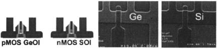
Figure 10. Schematics of the planar co-integration (pFET on GeOI and nFET on SOI on the same level, starting from localized Ge areas on SOI) and corresponding SEM picture of pFET and nFET.40

Figure 11. (a) Schematic principle of 3D monolithic co-integration with nMOS on SOI and pMOS on GeOI; (b) inverter transfer characteristic after co-integration.44
Figure 10 illustrates one Ge-based CMOS integration scheme involving planar FD-SOI Si nFETs and Ge pFETs. The Ge enrichment technique can create substrates with Si and Ge regions,40 adapted to this planar co-integration. An optional mobility booster is strain: tensile strain for Si nMOS and compressive strain for Ge pMOS.
Another possibility lies in 3D monolithic integration, illustrated in Fig. 11. Here the nMOSFETs are fabricated on SOI underneath the GeOI layer that is used for pMOSFET fabrication. The process can be summarized as follows. First, nMOSFETs are fabricated on an SOI substrate using a standard high temperature process. After interdielectric deposition and planarization, the Ge film is bonded using a low-temperature molecular process.41 This 3D co-integration scheme presents the unique advantage of enabling independent optimization of nMOS and pMOS devices. A two-step high-temperature nickel silicidation can be used for nFETs, whereas low temperature germanidation is required for pFETs. The first demonstration, based on a recrystallization technique, was published recently, demonstrating the feasibility of this approach.42
This solution is all the more interesting because it potentially leads to a gain in integration density and reduced interconnect delay. An SRAM technology with double-stacked Si layers, shown in Fig. 11(b), has already been demonstrated.43 Promising 4T-SRAM relying on the coupling between the two stacked layers show enhanced stability and density with respect to other double-gate like architectures.44 Thus, in conclusion, combining performance gains of GeOI pMOSFETs with monolithic 3D integration advantages promises simultaneous improvements at both the transistor and circuit level.
5. Innovative devices on GeOI: TFETs and nanowires
In order to further lower the power supply voltage VDD, a device based on an alternative operation principle, with a turn-on characteristic sharper than the 60 mV/decade MOS limit, would be very helpful. One such device is the tunneling field-effect transistor (TFET), where the gate voltage controls the interband tunneling between source and drain, and IOFF is not limited by source-drain diffusion. The fundamental idea of the TFET dates back to a proposal by Shockley and Hooper of a gated pn junction operated in avalanche mode. Experimentally, TFETs have been realized in III-Vs,45 bulk Si,46 SOI,47 and even carbon nanotubes.48 Recent simulations indicate that TFETs can have a sharper turn-on characteristic than CMOS transistors,49 attracting significant interest in the main-stream VLSI community. In SOI, reports of TFETs with S < 60 mV/decade have been published,50,51 with S reaching 42 mV/decade over a limited range of VG.
The principle of operation of the TFET is explained using the schematic band diagrams in Fig 12. The TFET is an ambipolar device that can operate in two modes depending on the gate bias, with interband tunneling occurring at either the source-channel or the drain-channel junction, although one of the two modes can be suppressed by asymmetric junction engineering. Since both ION and IOFF are largely determined by the tunneling through an interband barrier, they strongly depend on the maximum electric field EMAX (arising from the built-in junction field combined with the VD and VG-induced field components), as well as the channel bandgap EG.
Due to the relatively large bandgap of Si (EG ~ 1.1 eV), Si-based TFETs, whether SOI or bulk, suffer from relatively low ION·50,51 Taking advantage of the narrower Ge bandgap, a TFET in GeOI is in principle expected to exhibit enhanced tunneling ION. Such devices have been reported recently.52,53 Figure 13(a) shows the ID(VG) characteristics of a GeOI TFET biased at VD = 0.8 V, compared with SOI and SGOI TFETs.50 The GeOI TFETs show improved I0N currents, albeit with degraded S and IOFF. Figure 13(b) shows ID(VG) characteristics of a GeOI TFET with an epitaxial junction (see schematic in figure inset) at various drain biases VD. In principle, the epitaxial junction should be more abrupt than the standard counterdoped TFET junctions produced by implantation, and the resulting ION is indeed improved, but again at the expense of an inferior S. The same material and interface quality issues that have negatively impacted the performance of GeOI-based CMOS transistors are likely responsible. Note that the architecture enhancements used to improve CMOS performance may likewise benefit TFETs. Thus, Si or Ge nanowires (NWs) offer a promising platform for TFET fabrication. Recently, 3D stacked NW configurations in SOI have been reported with excellent FET characteristics:54 high ION, low IOFF, near-ideal 5 and reduced drain-induced barrier lowering. This type of device layout promises not only superior CMOS, as well as interesting hybrid integration possibilities,55 but also a platform for high-performance TFET fabrication. In fact, TFETs have been experimentally demonstrated in in-situ doped Si NWs grown by vapor-liquid-solid growth,56 and in scalable vertical Si NWs,57 showing excellent ION/IOFF ratios.
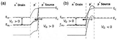
Figure 12. Band diagrams illustrating the interband tunneling in an ambipolar TFET for VD > 0 (reverse bias on the pn source-drain junction), (a) For VG > 0, electrons tunnel from the valence band of the p+-source into the inversion layer of the channel; (b) for VG < 0 electrons tunnel from the accumulation layer of the channel to the conduction band of the n+-drain. In both cases, dashed lines show the VD = VG = 0 band alignment.
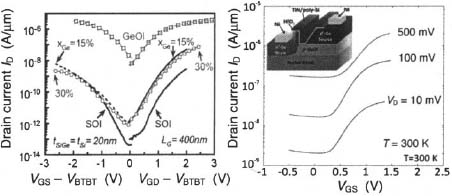
Figure 13. (a) Room-temperature lD(VG) characteristics of the GeOI TFET compared to SOI and SGOI TFETs at VD = 0.8 V;50 (b) epitaxial GeOI TFET characteristics at several VD values with the device structure shown in the inset.52
Taking advantage of the narrower Ge bandgap, a Ge NW-based TFET is expected to work even better, exhibiting higher current drive. Although Ge NW TFETs have not yet been fabricated, high-quality stacked Ge NWs have been reported58 using selective etching techniques analogous to those employed for stacked Si NWs – see Fig. 14.

Figure 14. Stacked Ge nanowires (NW) made on GeOI using similar etching techniques to those employed tor Si NWs.58
6. Conclusions
High-quality GeOI substrates can be produced using both Smart-Cut™ and enrichment techniques. Lower defect densities and Ge/BOX interface passivation are the main benefits of the Smart-Cut™ approach, while enrichment can provide ultrathin and compressively strained Ge layers. Process steps optimization permits the fabrication of high performance 70 nm gate length pMOSFETs on GeOI using high-K and Si/SiOx passivation. However several challenges like access resistance, off-state leakage and interface quality remain before GeOI-based devices can reach ITRS specifications for a possible high-power application. To overcome the currently insufficient performance of Ge-based nMOSFETs, Si/Ge co-integration schemes have been developed: vertically using Smart-Cut™ and laterally using Ge enrichment. This co-integration opportunity is a strong advantage for GeOI substrates compared to bulk technologies. Finally, the realization of innovative devices such as Ge nanowires and TFETs can open a path for GeOI in the field of ULSI integration and beyond-CMOS technologies.
Acknowledgments
The work at IMEP and CEA-LETI has been partially carried out within the EUROSOI+ network and Nanosil project ICT-216171. The work at Brown has been supported by the National Science Foundation (ECCS-0701635). One of the authors (A. Z.) gratefully acknowledges support under the RTRA program of the Nanosciences Foundation of Grenoble.
References
1. International Technology Roadmap for Semiconductors (ITRS), 2008 Update Emerging Research Devices (ERD) section.
2. P. Benkart, A. Kaiser, A. Munding, et al, “3D chip stack technology using through-chip interconnections,” IEEE Design Test Comp. 22, 512 (2005).
3. H. Shang, M. Frank, E. Gusev, et al., “Germanium channel MOSFETs: Opportunities and challenges,” IBM J. Res. Develop. 50, 377 (2006).
4. T. Akatsu, C. Deguet, L. Sanchez, et al., “Germanium-on-insulator (GeOI) substrates: A novel engineered substrate for future high performance devices,” Mater. Sci. Semicond. Processing 9, 444 (2006).
5. S. Cristoloveanu and S. Li, Electrical Characterization of Silicon-on-Insulator Materials and Devices, Boston: Kluwer Academic Publishers, 1995.
6. J. Mitard, B. De Jaeger, F. E. Leys, et al., “Record ION/IOFF performance for 65 nm Ge pMOSFET and novel Si passivation scheme for improved EOT scalability,” Tech. Digest IEDM (2008), art. 4796837.
7. A. Dimoulas and T. Tsipas, “Germanium surfaces and interfaces,” Micro-electronic Eng. 86, 1577(2009).
8. W. Van Den Daele, E. Augendre, K. Romanjek, et al., “Low-temperature measurements on germanium-on-insulator pMOSFETs: Evaluation of the background doping level and modeling of the threshold-voltage temperature dependence,” ECS Trans. 19, 145 (2009).
9. P. Broqvist, A. Alkauskas, and A. Pasquarello, “Defect levels of dangling bonds in silicon and germanium through hybrid functional,” Phys. Rev. B 78, 075203 (2008).
10. R. Xie, T. H. Phung, W. He, et al., “High mobility high-κ/Ge pMOSFETs with 1 nm EOT – New concept on interface engineering and interface characterization,” Tech. Digest IEDM (2008), art. 4796703.
11. Y. Nakakita, R. Nakane, T. Sasada, H. Matsubara, M. Takenaka, and S. Takagi, “Interface-controlled self-aligned source/drain Ge pMOSFETs using thermally-oxidized GeO2 interfacial layers,” Tech. Digest IEDM (2008), art. 4796838.
12. F. Letertre, C. Deguet, C. Richtarch, et al., “Germanium on insulator (GeOI) structures realized by the Smart-Cut™ technology,” Proc. MRS 809, 153 (2004).
13. C. Deguet, C. Morales, J. Deschamp, et al., “Germanium on insulator (GeOI) structures realized by the Smart-Cut™ Technology,” Proc. IEEE SOI Conf. (2004), pp. 96–97.
14. J. C. Bean, L. C. Feldman, A. T. Fiory, S. Nakahara, and I. K. Robinson, “GexSi1-x/Si strained layer supperlattice grown by molecular beam epitaxy,” J. Vac. Sci. Technol. A 2, 436 (1984).
15. J. F. Damlencourt and R. Costa, European Patent 0601850.
16. Z. Di, M. Zhang, W. Liu, et αl., “Fabrication and mechanism of relaxed SiGe on insulator by modified Ge condensation,” J. Vac. Sci. Technol. B 23, 1637 (2005).
17. J. F. Damlencourt, Y. Campidelli, Q. T. Nguyen, et al., “Epitaxial regrowth of Ge on SGOI and GeOI substrates obtained by Ge condensation,” ECS Trans. 6, 315(2007).
18. G. Ghibaudo, “New method for the extraction of MOSFET parameters,” Electronics Lett. 24, 543 (1998).
19. G. Hamaïde, F. Allibert, H. Hovel, and S. Cristoloveanu, “Impact of free-surface passivation on silicon-on-insulator buried interface properties by pseudotransistor characterization,” J. Appl. Phys. 101, 114513 (2007).
20. T. Signamarcheix, F. Allibert, F. Letertre, T. Chevolleau, L. Sanchez, and E. Augendre, “Germanium oxynitride GeOxNy as a back interface layer for GeOI substrates,” Appl. Phys. Lett. 93, 022109 (2008).
21. J. M. Hartmann, H. Grampeix, and L. Clavelier, “Epitaxial growth of thick Ge layers on nominal and 6° off Si (001): Ge surface passivation by Si,” ECS Trans. 16, 583 (2008).
22. E. Augendre, L. Sanchez, W. Van Den Daele, et al., “Demonstration of compressively-strained GeOI using the Smart-Cut™ technology,” submitted to IEEE SOI Conf. (2009).
23. Q. T. Nguyen, J. F. Damlencourt, B. Vincent, et al., “High-quality germanium-on-insultor wafers with excellent hole mobility,” Solid State Electronics 51, 1172(2007).
24. E. Augendre, L. Sanchez, L. Benaissa, et al., “Challenges and progress in germanium-on-insulator materials and device development towards ULSI integration,” ECS Meeting Abs. 902, 2387 (2009).
25. L. Lachai, J. Chiaroni, C. Le Royer, et al., “Resist stripping process on germanium: A basic post-implant study,” ECS Trans. 3, 113 (2006).
26. K. Romanjek, L. Hutin, C. Le Royer, et al., “High performance 70 nm gate length germanium-on-insulator pMOSFET with high-κ/metal gate,” Solid State Electronics 53, 723 (2009).
27. C. Le Royer, X. Garros, C. Tabone, et al, “Germanium/HfO2/TiN gate stacks for advanced nodes: Influence of surface preparation on MOS capacitor characteristics,” Proc. ESSDERC (2005), pp. 97–100.
28. V. Mazzocchi, S. Koffel, C. Le Royer, et al., “Experimental investigation of the impact of implanted phosphorus dose and anneal on dopant diffusion and activation in germanium,” Proc. MRS 1070, 35 (2008).
29. L. Hutin, S. Koffel, C. Le Royer, et al., “Activation level in boron-doped thin germanium-on-insulator (GeOI): Extraction method and impact of mobility,” Mater. Sci. Semicond. Proc. 11, 267 (2009).
30. C. Le Royer, L. Clavelier, C. Tabone, et al, “0.12 μm p-MOSFETs with high-κ and metal gate fabricated in a Si process line on 200 mm GeOI wafers,” Proc. ESSDERC (2007), pp. 458–461.
31. W. Van Den Daele, E. Augendre, C. Le Royer, J. F. Damlencourt, B. Grandchamp, and S. Cristoloveanu, “Low temperature characterization and modeling of advanced GeOI pMOSFETs: Mobility mechanisms and origin of the parasitic conduction,” to appear in Solid State Electronics (2010).
32. C. Le Royer, C. Tabone, K. Romanjek, et al, “105 nm gate length p-MOSFETs with high-κ and metal gate fabricated in a Si process line on 200 mm GeOI wafers,” Solid State Electronics 52, 1285 (2008).
33. L. Clavelier, J. F. Damlencourt, C. Le Royer, et al., “High hole mobility GeOI pMOSFETs with high-κ/metal gate on Ge condensation wafers,” Proc. SOI Conf. (2007), pp. 19–20.
34. J. L. Pelloie, D. K. Sadana, H. J. Hovel, et al., “Effect of the back gate conduction on 0.25 μm SOI devices,” Tech. Digest IEDM (1994), pp. 653– 656.
35. L. Clavelier, C. Deguet, C. Le Royer, et al., “Review of some critical aspects of Ge and GeOI Substrates,” ECS Transactions 3, 789 (2006).
36. T. Yamamoto, Y. Yamashita, M. Harada, et al, “High performance 60 nm gate length germanium p-MOSFETs with Ni germanide metal source/drain,” Tech. Digest IEDM (2007), pp. 1041–1043.
37. G. Nicholas, B. De Jaeger, D. P. Brunco, et al., “High-performance deep submicron Ge pMOSFETs with halo implants,” IEEE Trans. Electron Dev. 54, 2503 (2007).
38. G. Hellings, J. Mitard, G. Eneman, et al, “High performance 70-nm germanium pMOSFETs with boron LDD implants,” IEEE Electron Dev. Lett. 30, 88 (2009).
39. E. Batail, S. Monfray, C. Tabone, et al., “Localized ultrathin GeOI: An innovative approach to germanium channel MOSFETs on bulk Si substrates,” Tech. Digest IEDM (2008), pp. 397–400.
40. B. Vincent, J. F. Damlencourt, Q. T. Nguyen, et al., “The Ge condensation technique: A solution for planar SOI/GeOI co-integration for advanced CMOS technologies?” Mater. Sci. Semicond. Processing 11, 205 (2008).
41. J. P. Joply, O. Faynot, and L. Clavelier, “Three-dimensional CMOS integrated circuit and manufacturing method,” European Patent EP1811567.
42. J. Feng, Y. Liu, P. B. Griffin, and J. D. Plummer, “Integration of germanium-on-insulator and silicon MOSFETs on a silicon substrate,” IEEE Electron Dev. Lett. 27, 911(2006).
43. S. M. Jung, H. Lim, C. Yeo, et al, “High speed and highly cost effective 72 Mb density S3 SRAM technology with doubly stacked Si layers, peripheral only CoSix layers and tungsten shunt W/L scheme for standalone and embedded memory,” Tech. Dig. VLSI Symp. (2007), p. 82.
44. P. Batude, M. A. Jaud, O. Thomas, et al., “3D CMOS integration: Introduction of dynamic coupling and application to compact and Robust 4T SRAM,” Proc. ICICDTConf. (2008), pp. 281–284.
45. T. Uemura and T. Baba, “First observation of negative differential resistance in surface tunnel transistors,” Japan. J. Appl Phys. 33, 207 (1994).
46. W. M. Reddick and G. A. J. Amaratunga, “Silicon surface tunnel transistor,” Appl Phys. Lett. 67, 494 (1995).
47. C. Aydin, A. Zaslavsky, S. Luryi, et al., “Lateral inteband tunneling transistor on silicon-on-insulator,” Appl Phys. Lett. 84, 1780 (2004).
48. J. Appenzeller, J. Knoch, M. Radosavljević, and Ph. Avouris, “Multimode transport in Schottky-barrier carbon-nanotube field-effect transistors,” Phys. Rev. Lett. 92, 226802 (2004).
49. Q. Zhang, W. Zhao, and A. Seabaugh, “Low-subthreshold swing tunnel transistor,” IEEE Elecron Dev. Lett. 27, 297 (2006).
50. W. Y. Choi, B.-G. Park, J. D. Lee, and T.-J. King Liu, “ Tunneling field-effect transistors (TFETs) with subthreshold swing (SS) less than 60 mV/dec,” IEEE Electron Dev. Lett. 28, 743 (2007).
51. F. Mayer, C. Le Royer, J. F. Damlencourt, et al, “Impact of SOI, Si1-xGexOI and GeOI substrates on CMOS compatible tunnel FET performance,” Tech. Digest IEDM (2008), pp. 163–166.
52. T. Krishnamohan, D. Kim, S. Raghunathan, and K. Saraswat, “Double-gate strained-Ge heterostructure tunneling FET (TFET) with record high drive currents and <60 mV/dec subthreshold slope,” Tech. Digest IEDM (2008), art. 4796839.
53. D. Kazazis, P. Jannaty, A. Zaslavsky, et al, “Tunneling field-effect transistor with epitaxial junction in thin germanium-on-insulator,” Appl Phys. Lett. 94, 263508 (2009).
54. C. Dupré, A. Hubert, S. Bécu, et al., “15 nm-diameter 3D stacked nanowires with independent gate operation: ΦFET,” IEDM Tech. Digest (2008), art. 4796805.
55. T. Ernst, L. Duraffourg, C. Dupré, et al, “Novel Si-based nanowire devices: Will they serve ultimate MOSFETs scaling or ultimate hybrid integration?” IEDM Tech. Digest (2008), art. 4796804.
56. M. T. Björk, J. Knoch, H. Schmid, H. Riel, and W. Riess, “Silicon nanowire tunneling field effect transistors,” Appl Phys. Lett. 92, 193504 (2008).
57. Z. X. Chen, H. Y. Yu, N. Singh, et al., “Demonstration of tunneling FETs based on highly scalable vertical silicon nanowires,” IEEE Electron Dev. Lett. 30, 754 (2009).
58. E. Saracco, J.-F. Damlencourt, D. Lafond, et al., “Fabrication of suspended Ge-rich nanowires by Ge condensation technique for multi-channel devices,” ECS Trans. 19, 207 (2009).