Directed Self-Assembly – A Controllable Route to Optical and Electronic Devices Based on Single Nanostructures
Institute for Microstructural Sciences, National Research Council Ottawa, Canada, K1A 0R6
1. Introduction
Self-assembled semiconductor quantum dots offer an extremely attractive route to electronic structure control. Size, shape, composition and strain can all be used to tune the electronic structure of individual dots. Although useful, this versatility can also be a major drawback; particularly in devices where one would wish to couple to an individual dot or in situations where one would like many identical copies of a particular single dot structure. By the very nature of the self-assembled growth process, the characteristics of individual dots can vary widely and their spatial location is generally uncontrolled. In this chapter, we show how these limitations may be overcome and present examples in which control structures, such as optical microcavities or electrostatic gates, are constructed around individual quantum dots in an effort to determine their coupling to the optical field or to tune their electronic structure. Using such techniques one can engineer the symmetries of individual dots, introduce optical transitions that were previously forbidden, and so facilitate the construction of devices for the emission of single and entangled photon pairs.
2. Directed self-assembly
In certain compressively strained semiconductor materials systems, three-dimensional islands, or quantum dots (QDs), can be nucleated spontaneously in a so-called Stranski-Krastanow self-assembly process.1 It is possible to gain considerable control over this nucleation process if one can influence the surface migration behavior of adatoms deposited upon the crystal surface during growth.2,4 Fig. 1 illustrates one possible route to achieve the necessary control over surface diffusion processes: crystal growth, in this case chemical beam epitaxy (CBE) of InP,5 is initiated on an (001) oriented InP wafer that is patterned with openings in an otherwise continuous SiO2 mask. Under the appropriate conditions, InP growth on such a masked substrate produces deposition only on the areas of exposed semiconductor substrate, resulting in defect free InP nanotemplates with a (001) top surface and sloping sidewalls.

Figure 1. Schematic illustration of single, site-selected InAs/lnP QD growth. In (a), the underlying InP substrate is patterned with square openings in an otherwise continuous SiO2 masking layer. For openings with <100> edges, subsequent growth (b) produces square-based, pyramidal InP nanotemplates with {011} side facets. In (c), further InP growth results in a controlled reduction of the available (001) top surface area. In (d), deposition of InAs on the nanotemplate produces a single QD nucleated at the pyramid apex. Subsequent capping of the dot with InP produces a high-quality, optically-active InAs/lnP QD whose position is known with high precision.
The crystallographic orientation of these sidewalls is determined by the alignment of the oxide window: for example, square openings with edges directed along the <100> crystal directions will produce square based pyramidal InP nanotemplates with sloping {011} sidewalls. As the quantity of deposited InP increases, the nanotemplate height also increases, whilst the area of the (001) top surface decreases. In this manner, templates whose original dimension is of the order of a few square microns can be controllably grown until their top dimension approaches 50 x 50 nm; or the order of a typical QD dimension. If, at this point, the nanotemplate is exposed to the precursors for InAs growth, one finds that the deposited material migrates away from the {011} sidewalls to produce QD nucleation on the nanotemplate apex, as illustrated in Fig. 1. The beauty of this technique stems from the fact that the InP nanotemplate controlling quantum dot nucleation is prepared in-situ, in an ultrahigh-vacuum environment, with a size and geometry that is determined by the crystallography of the zincblende materials and by the quantity of InP deposited during nanotemplate growth. If the size and orientation of the original opening in the oxide is well controlled then the properties of the individual dots that are nucleated should also be well controlled. Fig. 2 below illustrates the level of control that can be achieved with the nanotemplate, directed self-assembly technique.

Figure 2. Scanning electron micrographs of uncapped InP nanotemplates with single InAs/lnP QDs nucleated at the apex. Top row, left to right, shows the effect on QD lateral dimension of decreasing the area of the available (001 ) top surface. Single QDs tend to fill the available (001) area, allowing direct size control. Bottom row, left to right, shows the effect on quantum dot symmetry of elongating the InP nanotemplate. This control of quantum dot geometry allows one to engineer the symmetries of electronic states within the quantum dot.
Using the nanotemplate, directed self-assembly technique, not only can one control the spatial location of the dot, but by carefully designing the size and shape of the InP nanotemplate, one is able to control the size and shape of the nucleated QD. Control of the dot dimensions allows tuning of the electronic structure and thus the emission energies and energetic degeneracies. This is of particular relevance to entangled photon pair generation for example,6,9 where the dot size and shape will determine whether the photon polarizations are entangled or merely correlated.10.
3. Spectroscopic signatures
Single InAs/lnP quantum dots can be designed for optical emission in the wavelength range between 1300 nm and 1550 nm (950 meV to 800 meV) and are consequently of interested for fiber-based optical communications.11 Fig. 3 shows typical luminescence12 from a single InAs/lnP quantum dot, as a function of increasing power from a HeNe pump laser.
At the lowest pump power (10 nW), a single optical emission line is observed corresponding to the annihilation of a single electron and single hole occupying the doubly degenerate s-shell of the quantum dot. It is this ground state emission that is of interest for single photon sources at telecom wavelengths and, as we shall see below, is directly tunable through choice of nanotemplate dimension. As a function of increasing pump power, successive electron-hole pairs are added to the quantum dot, revealing the rich many-body physics in play within these structures.13

Figure 3. Luminescence from a single InAs/lnP QD showing the development of electronic shell structure as a function of Increasing optical pump power.
Single dot spectroscopy is facilitated by the above-described nanotemplate self-assembly process in that individual pyramidal templates can be spaced many hundreds of microns apart upon a substrate surface and easily imaged with an optical microscope. Luminescence from a single nanotemplate can then be excited and collected using the same microscope objective, before being spectrally dispersed within a grating spectrometer and detected using a multi-element detector. Fig. 4 shows luminescence collected in this manner from a series of pyramidal templates with increasing base dimension. As the nanotemplate base dimension increases, the ground state luminescence energy from the quantum dot decreases as a result of diminishing electron and hole confinement.

Figure 4. Ground state luminescence from single InAs/lnP QDs on pyramidal nanotemplates of varying base dimension. The luminescence shifts to lower energy as a function of Increasing base width, at a rate of approximately 4.5 meV/nm.
4. Application of electric fields
• Vertical fields
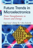
The quiescent charge state of a single QD can be controlled by the addition of Schottky gates to the sidewalls of a pyramidal nanotemplate, as illustrated in Fig. 5(a). In combination with an Ohmic back contact, Fig. 5(b), the four top gates can be used to apply an electric field in the vertical direction, raising or lowering the QD energy states with respect to the Fermi level.14,15 At large negative gate bias (VG= -1.8 V in Fig. 5(c)), the Fermi level lies below the QD electronic s-shell, producing an empty dot. In such circumstances, ground state optical emission from the dot corresponds to the neutral exciton X, as shown in the lowest spectrum of Fig. 5(c). At a gate bias of VG = –1.1 V, the Fermi level lies within the electronic s-shell, resulting in single electron charging of the quantum dot and the characteristic signature of a trion X–, in emission. When studied at high resolution, the optical emission from X and X– can be differentiated by virtue of the small (10– 100 μeV), exchange splitting present in the neutral exciton emission, producing a polarization-resolvable doublet. This splitting is absent for X–, since the initial state in the transition corresponds to a spin singlet pair of electrons and the final state to an unpaired electron. With a further reduction in the negative gate bias, VG = 0 in Fig. 5(c), an additional electron is added to the quantum dot to produce X2–.
Figure 5. (a) Scanning electron micrograph of a pyramidal InP nanotemplate with four Schottky gates; (b) schematic illustration showing the top gate metal, SiO2 dielectric, back gate and quantum dot position; (c) luminescence signal corresponding to three charge states of the quantum dot.

Figure 6. Effect of a lateral electric field on exciton and biexciton transitions within an InAs/lnP QD. Once the vertical field has been used to select the desired charge state of a dot, the lateral field can be used to introduce new transitions, or to engineer degeneracies between existing ones.
Ground state luminescence from X2– is again revealed as a doublet, corresponding to the two spin configurations of the final state (electrons in the s- and p-shells of the QD), although the low energy peak in Fig. 5 is very weak around 813 meV.
• Lateral fields
When differentially biased with respect to the back gate, the Schottky contacts of Fig. 6(b) can be used to apply a lateral electric field in the plane of the QD. Photoluminescence data from an InAs/lnP QD in such a lateral field is shown in Fig. 6(a), along with insets showing the effects of this field upon the electron and hole in-plane, parabolic confining potential.16,17,18 The lateral field separates the centers of electron and hole motion, introducing new optically allowed transitions and producing a red (Stark) shift of the single particle transition energies. An example of a normally forbidden optical transition can be observed around 984 meV in Fig. 6(a). This transition, which is observed under both directions of applied field, is associated with recombination from an s-shell electron and p-shell hole, a transition that is symmetry forbidden under zero applied bias.
Ideally, only ground state neutral exciton emission is observed under weak excitation conditions at zero applied bias. This is the situation in Fig. 6(a), with very weakly shifting neutral exciton emission observed around 978.5 meV. It is of interest to note that a single particle calculation of the expected Stark shift in these circumstances is grossly in error, with the predicted shift some two orders of magnitude larger than that observed in experiment. This phenomenon is explained by detailed many-body configuration interaction calculations, when it is observed that the reduction in electron-hole Coulomb interaction induced by charge separation almost completely compensates the expected single particle Stark shift for parabolic quantum dots. At first glance this compensation may be viewed as a detriment, since it removes one’s ability to tune the exciton emission energy; a feature that may be of interest in resonant optical devices. However, if the mechanism that compensates the excitonic stark shift is applied to the biexciton transition, XX, one finds that this transition blue shifts with increasing lateral electric field, as shown in Fig. 6(c). At some electric field the X and XX transition energies are expected to become degenerate. Under these circumstances, where the binding energy of the biexciton has been removed, it is possible to identify two indistinguishable paths for photon pair emission from the biexciton to exciton to vacuum cascade, and photon entanglement that is of interest for quantum key distribution can be engineered.
5. Optical cavities
The CBE growth technique described above for the preparation of site-selected InAs/InP quantum dots is also amenable to subsequent growth steps that allow single pyramidal templates to be planarized and further processed to produce photonic crystal microcavity membranes. A schematic view of the structure is given in Fig. 7(a), along with an SEM image of the final cavity design in Fig. 7(b).
Single missing hole, InP membrane cavities of the type shown in Fig. 7(b) have been fabricated with quality factors around 30,000 and mode volumes around half a cubic wavelength.19 With the ability to spatially align single InAs/InP QDs to the high field regions of these cavities, the potential exists to manufacture highly efficient single photon sources at telecom wavelengths, if one can match the cavity mode energy to the neutral exciton emission energy of the dot. At the present time, cavities with aligned single dots can be produced with quality factors of approximately 2,000, as shown in Fig. 7(c). The process used to planarize the pyramidal template produces a small local thickening of the final membrane around the template and shifts the cavity mode to slightly lower energy. This energy shift can be corrected and the cavity and exciton energies matched using a two stage process; for gross tuning, the surface of the cavity can be repeatedly oxidized and the resulting layer stripped, which has the effect of increasing the hole diameter and shifting the mode to higher energy.20 For fine tuning the cavity mode can be dynamically tuned by condensing small amounts of nitrogen gas onto the cavity surface at low temperature. An example of such tuning is shown in Fig. 7(d).
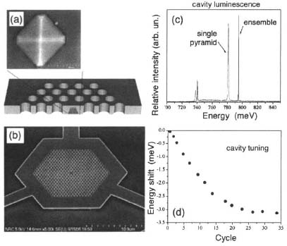
Figure 7. (a) Schematic illustration showing alignment of a site-selected single InAs/lnP QD within a photonic crystal microcavity membrane; (b) scanning electron micrograph of fabricated cavity; (c) optical emission from a microcavity with either a QD ensemble or a spatially aligned single pyramidal template; (d) fine tuning of the cavity mode using successive cycles of N2 condensation.
5. Conclusions
We discuss the application of directed self-assembly techniques to the production of single, site-selected InAs/lnP QDs. Single dots can be produced that emit efficiently in the wavelength range suitable for fiber-based communications and control structures can be built around them, such as electrostatic gates and photonic crystal microcavities, that allow fine tuning of their electronic properties and of their coupling to the optical field. The techniques that we describe form the basis for a manufacturable technology for the production of non-classical light sources.
Acknowledgments
The authors would like to acknowledge the financial support of the Canadian Institute for Advanced Research, the Canadian Institute for Photonic Innovations, Quantum Works, the Natural Sciences and Engineering Research Council, and the Business Development Bank of Canada.
References
1. I. N. Stranski and L. von Krastanow, Akad. Wiss. Lit. Mainz Math.-Naturwiss. K1. 11b 146, 797(1939).
2. R. Williams, G. Aers, P. Poole, J. Lefebvre, D. Chitrani, and B. Lamontagne, “Controlling the self-assembly of InAs/InP quantum dots,” J. Crystal Growth 223, 321(2001).
3. J. Lefebvre, P. J. Poole, J. Fraser, G. C. Aers, D. Chithrani, and R. L. Williams, “Self-assembled InAs quantum dots on InP nano-templates,” J. Crystal Growth 234, 391 (2002).
4. P. J. Poole, G. C. Aers, A. Kam, D. Dalacu, S. Studenikin, and R. L. Williams, “Selective growth of InP/InGaAs <010> ridges: Physical and optical characterization,” J. Crystal Growth 310, 1069 (2008).
5. P. J. Poole, J. McCaffrey, R. L. Williams, J. Lefebvre, and D. Chitrani, “Chemical beam epitaxy growth of self-assembled In/InP quantum dots,” J. Vac. Sci. Technol. B 19, 1467 (2001).
6. R. Seguin, A. Schliwa, S. Rodt, K. Pötchke, U. W. Pohl, and D. Bimberg, “Size-dependent fine-structure splitting in self-organized InAs/GaAs quantum dots,” Phys. Rev. Lett. 95, 257402 (2005).
7. R. J. Young, R. M. Stevenson, A. J. Shields, et al., “Inversion of exciton level splitting in quantum dots,” Phys. Rev. B 72, 113305 (2005).
8. A. Greilich, M. Schwap, T. Berstermann, et al., “Tailored quantum dots for entangled photon pair creation,” Phys. Rev. B 73, 045323 (2006).
9. N. Chauvin, B. Salem, G. Bremond, G. Guillot, C. Bru-Chevallier, and M. Gendry, “Size and shape effects on excitons and biexcitons in single InAs/InP quantum dots,” J. Appl. Phys. 100, 073702 (2006).
10. C. Santori, D. Fattal, M. Pelton, G. S. Solomon, and Y. Yamamoto, “Polarization-correlated photon pairs from a single quantum dot,” Phys. Rev. B 66, 045308 (2002).
11. D. Chithrani, R. L. Williams, J. Lefebvre, P. J. Poole, and G. C. Aers, “Optical spectroscopy of single, site-selected InAs/InP self-assembled quantum dots,” Appl. Phys. Lett. 84 978 (2004).
12. D. Kim, H. Lefebvre, J. Lapointe, M. E. Reimer, J. McKee, P. J. Poole and R. L. Williams, “Optical spectroscopy of single, planar, self-assembled InAs/InP quantum dots,” phys. stat. sol. (c) 3, 3840 (2006).
13. W. Sheng and P. Hawrylak, “Atomistic theory of electronic and optical properties of InAs/InP self-assembled quantum dots on patterned substrates,” Phys. Rev. B 72, 035326 (2005).
14. Μ. E. Reimer, D. Dalacu, J. Lapointe, et al., “Single electron charging in deterministically positioned InAs/InP quantum dots,” Appl. Phys. Lett. 94, 011108(2009).
15. M. E. Reimer, W. R. McKinnon, J. Lapointe, et al., “Towards scalable gated quantum dots for quantum information applications,” Physica E 40, 1790 (2008).
16. Μ. E. Reimer, M. Korkusinski, D. Dalacu, et al., “Prepositioned single quantum dot in a lateral electric field,” Phys. Rev. B 78, 195301 (2008).
17. M. E. Reimer, M. Korkusinski, D. Dalacu, et al., “Voltage induced hidden symmetry and photon entanglement generation in a single, site-selected quantum dot,” unpublished (arXiv:0706.1075vl [quant-ph]).
18. M. Korkusinski, M. E. Reimer, R. L. Williams, and P. Hawrylak, “Engineering photon cascades from multiexciton complexes in a self-assembled quantum dot by a lateral electric field,” Phys. Rev. B 79, 035309 (2009).
19. S. Frédérick, D. Dalacu, J. Lapointe, P. J. Poole, G. C. Aers, and R. L. Williams, “Experimental demonstration of high quality factor, x-dipole modes in InAs/InP quantum dot photonic crystal microcavity membranes,” Appl. Phys. Lett. 89, 091115 (2006).
20. D. Dalacu, S. Frederick, P. J. Poole, G. C. Aers, and R. L. Williams, “Postfabrication fine-tuning of photonic microcavities in InAs/InP quantum dot membranes,” Appl. Phys. Lett. 87, 151107 (2005).