Ultrafast Nanophotonic Devices For Optical Interconnects
VI-Systems GmbH, Hardenbergstrasse 7, D-10623 Berlin, Germany
1. Introduction
The ever-growing serial transmission speed of electrical interfaces is primarily driven by an increase in the microprocessor bandwidth caused by silicon scaling. As the density of transistors doubles every two years, the processor bandwidth increases, and the speed of the input/output (I/O) ports must increase. Moore’s Law for data communications predicts that a four-fold increase in the I/O speed is needed each 4-5 years. This scaling of speed imposes severe challenges to both copper and standard low-cost optical interconnects, which are presently limited to bit rates of ~10 Gb/s.
At the same time, according to the IEEE Ethernet Roadmap (Fig. 1) the single I/O bit rate should approach 100 Gb/s by 2017 while the aggregated transmission rate will increase to 5 Tb/s. At I/O speeds of 5–10 Gb/s, copper cables and connectors are becoming too energy consuming and bulky, so a massive deployment of optical interconnects is already starting.

Figure 1. IEEE Roadmap for the core and I/O bit rates.
*On leave from Ioffe Physical-Technical Institute of Russian Academy of Sciences, St. Petersburg 194021, Russia.
2. Recent progress in optical components
Very short-range optical links are presently served by multimode vertical-cavity surface-emitting lasers (VCSELs) as transmitters and PIN photodetectors as detectors. Previously it was believed that going beyond 10 Gb/s with VCSELs unavoidably causes problems with reliability and spectral quality. As a result, for example, the 17 Gb/s VCSEL bit rate was abandoned in the recent 2009 fiber channel standard in favor of a reduced 14 Gb/s rate.
To overcome the problems of conventional VCSELs several approaches have been proposed:
• “antiwaveguiding” VCSEL designs that suppress in-plane microdisk modes competing for the gain and also increase the strength of the main VCSEL transition;1
• the use of 850 nm quantum dots (QDs) that help to increase the differential gain, while localization of nonequilibrium carriers on QDs improves device reliability;
• advanced mask and oxide aperture designs enable devices with extremely low electrical parasitics, including capacitances as low as < 90 fF.

Figure 2. Bit error rate (BER) measurements for 9 μm-diameter oxide-confined VCSEL at a bias current of 9 mA and T = 20 °C. Insets: corresponding optical eye diagrams. Current density is ~5 kA/cm2 and the root-mean-square (RMS) spreading of the emission spectrum is < 0.3 nm. The measurements were made with 30 GHz receiver provided by Vl-Systems GmbH. “Open eye” means that “1” and “zero” signals are well separated for error-free transmission.
These new approaches have enabled VCSELs approaching 40 Gb/s bit rates at moderate current densities, shown in Fig. 2. Furthermore, these VCSELs appear sufficiently robust against degradation.2–4 Deconvolved VCSEL rise and fall times below 10 ps have been manifested up to 100 °C heat sink temperatures.
3. Novel modulation schemes
The use of VCSELs at speeds close to or beyond 40 Gb/s may still prove challenging. A reduced spectral width is needed at ultrahigh-speed transmission due to the fiber wavelength dispersion. High-speed single-mode VCSELs are based on very small oxide-confined apertures, operate at high current densities and are not reliable. Also, strategically we should look at solutions that keep the total transceiver power consumption below 2-4 mW/Gb/s for the complete optical link.
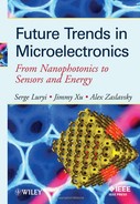
Figure 3. (a) Schematic view of an EOM DBR VCSEL device. The VCSEL section is operated in cw mode, whereas the EOM DBR section modulates the optical output signal; (b) electroluminescence intensity of a single-mode device as a function of applied reverse bias.
To fabricate VCSELs that can meet all these requirements we have proposed a vertical integration of a VCSEL with an electrooptic modulator (EOM), shown schematically in Fig. 3. The modulator section works under reverse bias, has ultralow capacitance and effectively serves as a “gate” to change the reflectivity of the top distributed Bragg reflector (DBR) section.5,6 Recently,6 we realized such an EOM DBR VCSEL, operating at a modulation voltage of ~2 V or less over a broad temperature range (20–100 °C). A modulator driver 1C for such a device having a 100 fF capacitance may consume <1 mW per Gb/s and the development of 40 Gb/s drivers and amplifiers is in progress.
At 2 V modulation, the extinction ratio is ~2 dB for a 1 μm aperture single mode devices, see Fig. 3(b). It increases to 3–5 dB in case quasi-single-mode or multimode devices at larger apertures. At high temperatures (85–100 °C) the extinction ratio increases further, by ~30%.
The electroluminescence and optical power of the integrated EOM DBR VCSELs are shown in Fig. 4. The prototype devices are capable of open eye data transmission at ~10 Gb/s, see Fig. 5. A single-mode EOM DBR VCSELs capable of 40 Gb/s transmission at low modulation voltage is presently in development.

Figure 4. Electroluminescence spectra at 2 mA (a) and 3 mA (b) current drive, together with light-current characteristics of the EOM DBR devices operating in single-mode (a, c) or quasi-single-mode (b, d) regimes with 1 μm and 2 μm oxide-confined apertures, respectively.

Figure 5. An open-eye diagram of the EOM DBR VCSEL with a 25 μm modulator mesa diameter (10 Gb/s, 25 °C). Average total power ~ 1 mW at ~1 V modulation voltage.
4. Integration of CMOS and III-V technologies
At bit rates exceeding 40 Gb/s the maximum signal distribution distance over a printed circuit board is limited to only a few centimeters or even less. Thus, optical transmitters and detectors must be placed as close as possible to the drivers and amplifier ICs, respectively. Preferably, the optical components must be directly integrated with the ICs.7 As illustrated in Fig. 6, the planar design of VCSELs and top-illuminated photodetectors provides a unique vertical integration opportunity within the standard CMOS technology, because wafer-separated devices can be effectively “printed” onto CMOS ICs. Further planarization and dielectric sealing will enable their integration into a scalable, massively parallel CMOS technology.7

Figure 6. (a) Wafer-separated VCSEL membranes hold promise of reliable cw operation when attached to a silicon wafer; (b) the small (~5 μm) membrane thickness is compatible with CMOS-based planarization technology.
4. Conclusion
We believe that VCSELs leveraged by novel nanophotonic concepts will provide a reliable source of interconnect technologies in the near future.
Acknowledgements
This chapter was written in cooperation with J. A. Lott and V. A. Shchukin (VI-Systems GmbH); A. Mutig, G. Fiol, T. Germann, and D. Bimberg (TU-Berlin); and A. Blokhin, L. Ya. Karachinsky, M. V. Maximov, and A. M. Nadtochiy (Ioffe Physical-Technical Institute and the Academic University of St. Petersburg, Russia).
References
1. J. Humphreys and J. Scaramella, “The impact of power and cooling on data center infrastructure,” IDC document #201722 (2006).
2. N. N. Ledentsov, J. A. Lott, V. A. Shchukin, et al., “Quantum dot insertions in VCSELs from 840 to 1300 nm: Growth, characterization, and device performance,” Proc. SPIE 7224, art. 72240P (2009).
3. J. A. Lott, V. A. Shchukin, N. N. Ledentsov, et al., “20 Gb/s error-free transmission with ~850 nm GaAs-based vertical cavity surface emitting lasers (VCSELs) containing InAs-GaAs submonolayer quantum dot insertions,” Proc. SPIE 7211, art. 721114 (2009).
4. A. Blokhin, J. A. Lott, A. Mutig, et al., “850 nm VCSELs operating at bit rates up to 40 Gb/s,” Electronics Lett. 45, 501 (2009).
5. V. A. Shchukin, N. N. Ledentsov, J. A. Lott, et al., “Ultrahigh-speed electro-optically modulated VCSELs: modeling and experimental results,” Proc. SPIE 6889, art. 68890H (2008).
6. N. N. Ledentsov, “Dots speed datacom VCSELs,” Compound Semicond. 15, 25 (2009).
7. J. A. Lott, “Fabrication and applications of lift-off vertical cavity surface emitting laser (VCSEL) disks,” Proc. SPIE 4649, 203 (2002).