
What Will Modern Photonics Contribute to the Development of Future Optical Communication Technology?
Dept. of Electrical and Telecommunications Engineering Technology, New York City College of Technology-CUNY, Brooklyn, NY 11201, U.S.A.
1. Introduction
Optical communications is the linchpin of modern telecommunications; in fact, the vast majority of global telecommunications traffic today is delivered optically, which means that optical communications laid the foundation for all the beneficial changes in our lives that the Internet now provides. The optical communications industry, in fact, is one of the largest consumers of electronic and photonic products; hence, developments in the optical communications area will, to a great extent, shape trends in electronics and photonics.
Optical communication today ranges widely in three dimensions: in space, in time, and in frequency (spectrum).
In space (that is, transmission distance), optical communication ranges from nanometers in optical interconnects to tens of thousands of kilometers in intercontinental links. In time, the optical communications industry operates from kilobits per second in short-reach connections to terabits per second in longdistance links; these bit rates correspond to characteristic times that range from milliseconds to picoseconds. In spectrum, optical communication covers the wavelength range from 850 nm (local) to 1650 nm (long-haul).
If this variety of the characteristics is insufficient to stress the complexity of modern optical communications, we must add another factor: the network. Delivering information to an individual receiver through a web of connections ranging from chip-level interconnects to the worldwide network is a herculean task. It involves intelligent firmware systems, advanced transmission technology and complex network management, all of which are controlled by quite sophisticated software.
Optical communication engineers are under constant pressure to improve all aspects of this technology – from the ever-increasing demand for bandwidth to reducing the bit-per-kilometer cost. Responding to these demands, they have developed many wonderful components, devices, and systems. However, today’s achievements will not guarantee the fulfillment of tomorrow’s tasks.
Optical communication, in its hardware layer, is a part of the photonics community, which is actively conducting fundamental and applied research to discover new phenomena and applications.To name just a few, these discoveries range from today’s experiments with single-photon manipulation (generation, modulation, transmission, and detection), to silicon-based photonics, to optically active integrated circuits, to photonic crystals, to quantum routers, to metamaterials and to nanophotonics. Such discoveries will transform the optical communication technology.
The purpose of this chapter is to depict the current status of optical communications, to stress its achievements, and to emphasize its needs. We will also discuss several examples of the latest developments in photonics that would enable the development of new components, devices, and systems for fiber-optic communications technology. The hope is that this presentation will stimulate some thoughts and new ideas that will result in the further development of photonics and optical communications.
2. Optical communications
• General consideration and the scale of operation
A basic fiber-optic communications system (link) is shown in Fig. 1(a). In general, the transmitter (Tx) is a device that launches an information signal into the optical fiber, which is the conductor of the optical signal, and the receiver (Rx) is a device that extracts information from the optical fiber in a suitable form. We need to remember that the goal of this system is to deliver information. Figure 1(b) shows the situation when light is delivered but information is lost because of the spreading of optical pulses caused by modal dispersion.1

Figure 1. Basics of optical communications: (a) block diagram of a fiber-optic communications link; (b) the goal is to deliver information, not light (DMD – differential mode delay; ISI – inter-symbol interference).
Over the last 30 years, optical communications has developed from a nonexistent technology to the linchpin of the telecommunications industry. Why? The main advantage of optical communications over any other means of transmission is speed. We have to distinguish between two speeds when delivering signals: propagation speed and transmission speed. Propagation speed measured in m/s is the area of interest for developers of on-chip-level optical interconnects; here, since photons move faster than electrons, optical communications offers the solution to interconnect delay. Transmission speed (transmission capacity, or bandwidth) measured in bit/s is proportional to the frequency of a carrier fC, and since light has the highest fC (hundreds of THz) of all the practical signal carriers, optical communications systems can achieve the highest transmission capacity and the highest values of bandwidth-distance product.
To better appreciate the scale of optical-communications technology, we need to consider three dimensions of its operation: space (distance), time (bit rate), and spectrum (range of wavelengths).
• Transmission distances in optical communications
Let us consider the range of transmission distances covered by optical communications today, as shown in Table 1.2 Since the cost/performance curve of optics is much steeper than that of electronics, optical communications has effectively replaced the electrical systems in long-distance, metro and access scales.
Figure 2 shows a version of the worldwide optical network map. This map does not show all of the intercontinental, let alone all terrestrial, networks; it does show, however, the global scale of optical communications.
Figure 3 shows an example of a metro-scale optical network developed by just one company, RCN Corporation, to cover New York City. One can only imagine how many similar networks cover this city.
An individual customer can optically access the global telecommunications infrastructure by means of a cable-TV network (CATV) or a passive optical network (PON), as illustrated in Fig. 4.
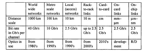
Table 1. Optical communications – transmission distances and applications.

Figure 2. Global optical network (from http://personalpages.machester.ac.uk/staff/m.dodge/cybergeography/atlas/cables.html).

Figure 3. An example of a metro-scale optical network: New York City (courtesy of RCN).

Figure 4. Optical access networks: cable-TV (CATV) network (top); passive optical network (PON) (bottom).
A CATV network is mostly fiber-based; however, there are still segments of coaxial-cable connections. In the United States, a cable-TV network is the primary provider of broadband access, whereas most of the developed world still relies on copper-based DSL technology. A passive optical network (PON) replaces the traditional copper-wire telephone connections from a dwelling to a central office. The installation of PON and other types of optical access networks keeps growing in the U.S. and other developed countries; as a matter of fact, in South Korea and Japan, optical access has become the main type of broadband connection.
Commercially available PONs (e.g., FiOS) are based on time-division multiplexing (TDM). The TDM technique is inherently restricted in bit rate; what is more, TDM-based PON has security and confidentiality issues that still have to be resolved. The natural solution would be the move to wavelength-division multiplexing (WDM). However, the classical WDM approach, as applied to PON, suffers from a major drawback: it is economically ruinous to keep an inventory of individual optical network terminals (ONTs), also called units (ONUs), for every customer – see Fig. 5(a). Instead, all customers must have the same type of ONT, which requires developing colorless ONTs, as shown in Fig. 5(b).3

Figure 5. Wavelength-division multiplexing PON: (a) classical approach; (b) colorless implementation.3
As we see, optical communications technology replaces copper everywhere, from worldwide to metro to access networks. Also, at the in-room and intra-rack scales, optical fiber has completely replaced copper wire; at the card-to-card and on-card scales, the fiber-optics links start to compete with the electrical links. The trend to replace copper at the chip level is made necessary by continual increases in the bit rate at the system (e.g., computer) and board levels. The movement in computer-system architecture from parallel data buses to high-speed serial I/Os is also in concert with the shift to optics. When the data rate changes from 10 Gb/s to 40 Gb/s and 100 Gb/s, the move to optical interconnects will become inevitable.
The classification of interconnects is based on their applications, which boils down to the interconnect lengths.2 Thus, we distinguish rack-to-rack (in-room), card-to-card, intra-card, intra-module (on-MCM), and intra-chip (on-chip) interconnects – see Table 1. Today’s electrical interconnects suffer from many problems:4–7 the small value of the bandwidth-length product, significant delay (~20–25 ps/mm), low noise immunity, crosstalk between channels, general noise, high power consumption (~1 mW/mm) accompanied by heat dissipation, and frequency-dependent losses. Also, there are architectural problems with electrical interconnects: the performance of the CPU and other electronic modules increases much faster than the transmission speed of the links among these modules. By some estimates, wire delay will increase 20 times faster than device-level gate delay.
Optical interconnects may be the solution to all these problems. Figure 6(a) shows an interconnect module that includes all main components shown in Fig. 1. Theoretically, optical interconnects will reduce delays (e.g., a delay might be as low as 4–5 ps/mm for a polymer and 10 ps/mm for Si waveguides8), will allow for 3D dense packaging thanks to low crosstalk (e.g., the minimum pitch is 8–9 μm for polymer and 0.5–1 μm for Si8), and will eliminate or reduce all other drawbacks of electrical interconnects in a similar manner.
There are several areas in the computer industry that are in dire need of optical interconnects. One of these is the area of supercomputers because they rely heavily on transmission between CPUs and memory and on card-to-card (inter-node) transmission. The companies involved in designing supercomputers are actively working on the development of optical interconnects,5,6 see Fig. 6. Another area where we expect the realization of chip-to-chip optical interconnects is microprocessors, because the microprocessor transition from multi-core to many-core architectures will drive chip-to-chip bandwidth demands. Future architectures will require bandwidths of 200 GB/s to 1.0 TB/s and will bring about the era of tera-scale computing. Currently, a DARPA program named UNIC is funding a five-year project (at Sun Microsystems) to develop microchip interconnectivity via on-chip optical networks based on silicon photonics and proximity communication.7

Figure 6. A Terabus optical interconnect: (a) cross-section of a Terabus module structure; (b) eye diagram at the output of a Terabus receiver with the optical input from a Terabus transmitter at 14 Gb/s; (c) a Terabus chip – an optical transceiver with CMOS driver and receiver chips coupled with lll-V optical components, the entire integrated package measures 3.25 by 5.25 mm.2

Figure 7. (a) Source and detector dies bonded onto an SOI wafer; (b) a fabricated chip with 10 PD blocks with eight devices per block (courtesy of Pietro Binetti9).
Figure 7 demonstrates examples of an optical interconnect fabricated in the research laboratory, their operation, and their dimensions. Bear in mind that card-to-card optical interconnects are commercially available.
To sum up our discussion of the scale of operation of optical communications, it is clear that optical communication consistently outperforms its electronic counterpart over ever-shorter distances. For last twenty plus years, optical communications has replaced electronics in scales ranging from ultra-long-haul to rack-to-rack links. These replacements occur mainly in point-to-point topologies; this is why some researchers refer to optical interconnections rather than to networks. In any event, the trend is clear: optical interconnections are increasingly coming closer to inter-chip transmission.
• Time scaling in optical communications – TDM
The main advantage of optical fiber over any other transmission medium is its greater bandwidth (transmission capacity). This is why the primary objective in using optical communications has been and remains the increase in the bit rate of the transmitting signal. To discuss this topic, we need to distinguish between the bit rate (BR) of a single channel (at a given wavelength) achieved by time-division multiplexing (TDM) and the data rate (DR) transmitted over a fiber achieved by wavelength-division multiplexing (WDM). The DR for long-distance optical networks runs into tens of Tb/s, whereas metro optical networks operate at tens of Gb/s and access optical networks operate at a few Gb/s or hundreds of Mb/s.
Concerning the TDM BR, a single wavelength now routinely achieves a bit rate of 40 Gb/s. This has been accomplished by improving the performance of individual transmitters and receivers and combining (interleaving) several low-rate signals in one stream (e.g., four 10 Gb/s signals). The industry has been approaching a bit rate of 100 Gb/s.

Figure 8. Internal and external modulation techniques.
The TDM bit rate, as well as the transmission performance in general, depends very much on the modulation technique. In optical communications, we employ internal and external modulation schemes, as shown in Fig. 8. Modern laser diodes (LDs) do not allow for internal (direct) modulation at a high bit rate. External modulation keeps LDs in the comfortable cw regime and relegates all modulation problems to an external modulator. With this approach, the rate of 10 Gb/s is routinely achieved.1 Recently developed modulation schemes, such as quadrature phase-shift keying, overcome dispersion-caused signal degradation without recourse to dispersion-compensation modules, an industry advance that significantly reduces the cost of transmission. The use of an advanced modulation technique is an example of solving a problem with a component (here, the problem lies with the optical fiber) by resorting to a network-level approach.
• The spectrum of optical communications – WDM
We need to realize that TDM is inherently restricted in its bit rate. Indeed, for the bit rate of 1 Tb/s, the bit time is equal to 10”12 s or 1 ps. There are no photonic devices (LDs, modulators, or PDs) that can operate at this speed. Today’s electronics mainly operate at 10 Gb/s; modulation at 40 Gb/s has been achieved and modulation at 100 Gb/s is on the horizon. On the other hand, an optical fiber can carry 100 Tb/s on a single wavelength, which means that an optical fiber can carry a thousand 100 Gb/s channels.
The solution to this bottleneck is WDM, which allows for an n-fold increase in the data rate, where n is the number of wavelengths. An example of four-wavelength WDM and the corresponding frequency spectrum are shown in Fig. 9.
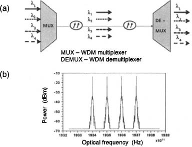
Figure 9. Schematic concept of WDM (a) and an example of a WDM frequency spectrum (b).

Figure 10.The spectrum and channel spacing of CWDM vs. attenuation length (DWDM operates over the C and L bands).
There are two types of WDM today: dense WDM (DWDM) and coarse WDM (CWDM). They differ in spacing between two adjacent channels (wavelengths): DWDM operates at spacing ranging from 1.6 nm (200 GHz) to 0.2 nm (25 GHz); CDWM works at 20 nm spacing. DWDM occupies the wavelengths from ~1530 nm to ~1610 nm, divided into a conventional band (C) 1530–1560 nm and a long band (L) 1560–1610 nm. CWDM ranges from 1271 nm to 1611 nm, and is also subdivided into a number of sub-sections, as illustrated in Fig. 10, together with the attenuation range that varies with wavelength.
An important metric of WDM is spectral efficiency SE, which is equal to the data rate divided by the spectral bandwidth SBW necessary to transmit this signal: SE (bit/s/Hz) = DR (bit/s)/SBW(Hz). Since DR = n times BR, SE becomes equal to BR divided by the channel spacing in Hz. For example, 10 Gb/s transmitted over 100 GHz bandwidth gives SE = 0.1 bit/s/Hz (very low), whereas 100 Gb/s transmitted over the same bandwidth gives SE = 1 bit/s/Hz (high). The goal is to increase SE as much as possible: a value as high as 1.32 bit/s/Hz has been achieved in a trial. The physics behind these numbers emphasizes that in reality there is a tradeoff between the BR of an individual channel and the spacing between two adjacent channels.
The WDM technique comes with its own problems, too. For one thing, we cannot launch as many channels as we want because the high power associated with many channels produces an unacceptable amount of nonlinear phenomena in the optical fiber. Another restriction on the number of channels derives from the fact that all WDM channels compete for the gain of an optical amplifier.10
• Optical communications – networks
A network differs from a point-to-point link by its ability to deliver a signal to every node out of many nodes or customers. This capability clearly indicates the need for switching and transmission protocols. A telecommunications network is the symbiosis of the physical and logical (intelligent) layers, very much similar to a computer, which is the symbiosis of hardware and software.The network’s physical layer is responsible mainly for transmission and switching, whereas the logical layer is responsible for implementing the network protocols. Obviously, the better the components, the better the network, but bear in mind that even ideal components cannot change a network’s topology or architecture.
There are two main network architectures today: circuit-switching and packet-routing. They are compared schematically in Fig. 11. The circuit-switching network establishes a dedicated line between end-users for the duration of their communication. This is how the public-switched telephone network (PSTN) still operates. The main drawback of this network is its very inefficient use of bandwidth. In contrast, the packet-routing network disassembles a message into separate packets, transmits these packets via any available route, and reassembles the packets into the original message before delivering it to an end-user. This transmission method is also known as IP, standing for Internet protocol, because the Internet operates by packet routing. Obviously, IP transmission maximally utilizes the network’s capacity; this is why the today’s trend in telecommunications is to move all types of transmission (voice, video, and data) in IP mode.

Figure 11. (a) Circuit-switching and (b) packet-routing network architectures.
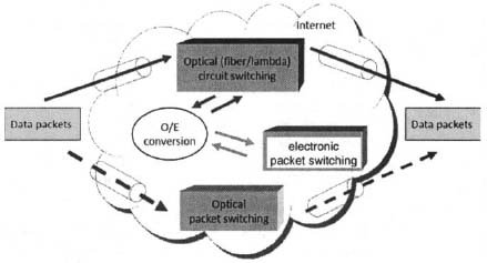
Figure 12. Internet traffic is delivered optically but routed electronically.
Optical networks are the backbone of the Internet; however, to support IP transmission over the optical network, we have to convert an optical signal into an electrical one and process (route) the packets electronically, converting them back into optical format for further transmission – see Fig. 12. This E/O/E conversion causes delays and significant expense; thus, the absence of optical packet routers is the main drawback of the optical network today. In spite of tremendous R&D efforts, optical packet routers are still far from a commercial reality – this is one of the major challenges confronting photonics researchers. There are many palliative solutions to this problem, such as using protocol-based approaches (specifically, generalized multiprotocol label switching) or employing hybrid networks in which all-through traffic is transmitted optically and add-drop messages are routed electronically. Nevertheless, IP over WDM transmission – which is how the optical-communications industry refers to it – still awaits all-optical implementation.
• Main problems of optical communications and their possible solutions
At this point we will consider the main problems of optical communications and their possible solutions from a top-down perspective, where top refers to a network and down to an individual component. From a physical layer standpoint, the network is a set of nodes connected by links. Nodes include systems, such as switches/routers, optical cross-connects, optical add/drop multiplexers, optical amplifiers, regenerators, etc. Systems, in turn, include modules, such as transmitters (Tx), receivers (Rx), dispersion-compensation modules, wavelength converters, etc. Modules include components, such as laser diodes, photodiodes, modulators, couplers/splitters, MUX and DEMUX, optical filters, attenuators, gratings, etc. The links include optical fiber and waveguides.10 Table 2 presents some of the strategic problems and their possible solutions.


Table 2. Problems facing optical communications and their possible solutions.
3. What will modern photonics contribute to the development of future optical communications technology?
Through research in photonics, we will discover new phenomena and new approaches to the development of devices and components that will be used in optical communications. Today’s research in photonics lays the foundation for physical layer of future optical networks. But which specific research results are likely to contribute specific devices and components for tomorrow’s optical communications networks is another matter. Nobody has a crystal ball and the goal of this chapter is simply to bring to the attention of the photonics research community the technology needs of the optical communications industry. Let us consider, from this standpoint, several examples of current research programs in photonics.
• Plasmonics
When an electromagnetic (EM) wave falls at the interface between a dielectric and a metal, polarization charges are created at the interface. The electrons in the metal will respond to this polarization, giving rise to surface plasmons – interface modes that have combined EM-wave and surface-charge properties. When light is coupled with surface plasmons, we have surface plasmon-polaritons,13 illustrated schematically in Fig. 13(a).
We see several potential applications for surface plasmons in optical communications. For one thing, the miniaturization of conventional photonic circuits is limited by the diffraction limit, such that the minimum feature size is of the order of a wavelength. Using surface plasmons, it may be possible to overcome the diffraction limit, which can lead to the miniaturization of photonic circuits. In general, using surface plasmons can open the door to practical applications of nano-optics, where the main problem today is delivery and concentration of optical radiation energy caused by the ratio of optical wavelength (hundreds of nm) to characteristic length of nano-optical devices (nm).13
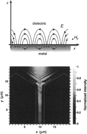
Figure 13. (a) Schematic illustration of a surface plasmon; (b) light propagation in a plasmonic waveguide.13
Figure 13(b) demonstrates light propagation in a plasmonic waveguide that could potentially serve in on-chip optical interconnects. A waveguide, over a centimeter in length with low bending loss has been demonstrated.14
Overcoming the diffraction limit with the help of surface plasmons paves the way for beam shaping, making it possible to design near-field and far-field patterns almost at will, which would allow for optical processing and coupling light into nanostructures.15 Some recent results in surface-plasmon research of particular relevance to the optical communications community include:
• the potential of surface plasmons to be switched at THz rates and consume mJ/cm2 power for modulation, which might lead to the creation of new types of modulators and all-optical switches;
• the fabrication of plasmonic LEDs that approach 10-GHz modulation bandwidth; this might lead to using LEDs for optical interconnects;
• the creation of a visible plasmon laser, which in turn could result in the development of new light sources for nanoscale optics;
• the development of a plasmonic lens that greatly increases photodetection capability and offers the potential for new types of photodetectors.
In general, surface plasmons engender new hope for the development of integrated devices that will perform all of their operations optically.
• Photonic crystals (semiconductors of light)
Photonic crystals are structures consisting of alternating thin layers of two dielectric materials with different refractive indexes; these layers reflect radiation within a resonant band and transmit other wavelengths.16 The resonantly reflected band of wavelengths is known as the “photonic bandgap”, in analogy to the electronic bandgap. The value of the photonic bandgap depends on two parameters of the dielectric layers: their thicknesses and refractive indexes. Since photons cannot propagate through solid matter if their energies fall in the photonic bandgap, photonic crystals can confine light in three dimensions.
The main applications of photonic crystals in optical communications are associated with photonic-crystal fibers. These fibers cannot serve as transmission media because they introduce huge losses, but – thanks to their special properties – they can be used for building fiber lasers, amplifiers, and nonlinear devices, which could provide dispersion control and compensation, filtering, and switching. In addition to the advantages provided by photonic-crystal fibers, optical communications could benefit from other results of the ongoing research in this area. For example, photonic-crystal lasers – which have a low-threshold current and high-speed modulation – could be employed in optical interconnects. What is more, photonic crystals potentially allow for creating tunable devices that would dramatically change the landscape of optical communications. They also could lead to the development of optical-processing devices, such as switches, photonic memory devices, and wavelength converters, the latter potentially operating at the single-photon level. Eventually, silicon photonic crystals could lead to integrated optical devices on the silicon-on-insulator (optical chip) platform, the holy grail of optical communications.17
• Use of single photons in communications?
Signals encoded in a single photon promise the absolute minimum in power consumption – and therefore cost – for generation, modulation, transmission, and detection. But can we ever really operate with a single photon for communications? Considering all the main operations occurring in sequence, we can say that the generation and detection of a single photon is a difficult but achievable task.18 As for modulation, recently the modulation of a single photon with an arbitrary waveform was reported by Kolchin and co-workers.18,19
Also, an experiment confirming the feasibility of establishing a link between an orbiting source of single photons and a ground telescope was conducted recently. In this experiment, a single photon was sent and received over 150 km. Weak laser pulses were directed toward orbiting satellites that mirror optical signals on an exact parallel return path to the source. The chosen transmission parameters caused less than one photon per pulse to be returned on average, thus simulating a single-photon source. Because the signal traveled through only 8 km of the Earth’s atmosphere out of a total distance of 160 km, the link has been established without serious atmospheric or geographic disturbances.20
In the transmission of a signal photon over a photonic crystal fiber, nonlinear effects were observed at the lowest power level, a finding that may lead to the development of all-optical processing devices.21
Clearly, it is impossible to even mention all the areas of photonics research under way today and obviously, it is a long way from laboratory experiments to practical technology; however, the described results provide hope and a direction that further efforts will take.
4. Conclusions
Tremendous progress in all areas of optical-communications technology has been achieved over the last two decades, including:
• significant progress in the integration of components and modules;
• advances insophisticatedandefficientmodulationtechniquesand devices;
• transmission speeds of tens of Tb/s with spectral efficiency approaching its fundamental limit due to advances in WDM technology;
• dramatic reduction of cost per bit, which continues to decrease, making optical communications competitive at smaller and smaller distances.
At the same time, modern photonics is constantly discovering new phenomena and processes, some examples of which we briefly discussed above.
Our discussion shows that photonics and optical communications benefit from mutual fruitful cooperation. The linkup of these two fields promises progress towards the hypothetical ideal optical communications system: one that works on any scale, at any transmission speed, and over any part of the spectrum. Figure 14 illustrates this point by showing an ideal optical communications network that accepts a signal in any format and, after changing it to an optical form, seamlessly delivers the signal to any required point and in any required format. On the other hand, the research currently in progress in various photonics areas will bring new ideas and concepts to a technology that will one day boast such an ideal optical network.
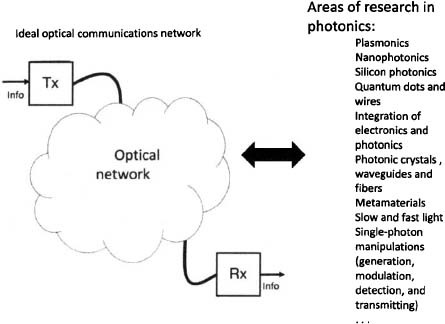
Figure 14. Ideal optical network and areas of research in photonics.
Optical communications and fundamental research in photonics are closely interconnected and therefore inspire and motivate researchers in these respective fields to pursue further advances. Only time will tell what results of today’s photonics research will turn up in tomorrow’s optical communication products.
References
1. Djafar K. Mynbaev and Lowell L. Scheiner, Fiber-Optic Communications Technology, Upper Saddle River, NJ: Prentice Hall, 2001.
2. A. F. Benner, M. Ignatowski, J. A. Kash, D. M. Kuchta, and M. B. Ritter, “Exploitation of optical interconnects in future server architectures,” IBM J. Res. Develop. 49, 755 (2005).
3. P. Chanclou, F. Payoux, T. Soret, et al., “Demonstration of RSOA-based remote modulation at 2.5 and 5 Gb/s for WDM PON,” Proc. Optical Fiber Commun. Conf. (2007), art. 4348854.
4. I. T. Young, E. Mohammed, J. Liao, et al., “Optical I/O technology for tera-scale computing,” Tech. Dig. ISSCC (2009), art. 4977511.
5. Y. Vlasov, “Silicon photonics for next generation computing systems,” www.ecoc2008.org/documents/SC2_Vlasov.pdf
6. K. Takeuchi, “Technical trends in optical interconnection technology – Towards its implementation in the ‘Keisoku’ supercomputer,” http://www.nistep.go.jp/achiev/ftx/eng/stfc/stt020e/qr20pdf/STTqr2002.pdf
7. G. Overton, “Can optical integration solve the computational bottleneck?” Laser Focus World 45, 64 (March, 2009).
8. B. Jalali, S. Fathpour, and K. Tsia, “Green silicon photonics,” Optics Photon. News 20, 18 (June, 2009).
9. P. R. A. Binetti, J. Van Campenhout, X. J. M. Leijtens, et al., “An optical interconnect layer on silicon,” Proc. 13th Europ. Conf. Integr. Optics (2007), pp. 1-3.
10. Djafar K. Mynbaev, “The physical layer of the optical networks: Devices and subsystems,” Online Tutorials IEEE Commun. Soc. (2006), www.comsoc.org/tutorialsnow
11. G. Shen and R. S. Tucker, “Energy-minimized design for IP over WDM networks,” J. Optical Commun. Networking 1, 176 (2009).
12. M. Haurylau, G. Chen, H. Chen, et al., “On-chip optical interconnect roadmap: Challenges and critical directions,” IEEE J. Selected Topics Quantum Electronics 12, 1699 (2006).
13. I. Zozoulenko, “Surface plasmons and their applications in electro-optical devices,” Linköping Univ. (2006), http://www.itn.liu.se/meso-phot
14. S. Park, “Polariton waveguide has low bending loss,” Laser Focus World 45, 9 (February, 2009).
15. F. Capasso, N. Yu, E. Cubukcu, and E. Smythe, “Using plasmonics to shape light beams,” Optics Photonics News 20, 22 (May, 2009).
16. J. Heght, “Photonic crystals foster a burst of innovation,” Laser Focus World 45, 103 (January, 2009).
17. C. Lopez, “Fabrication techniques for silicon photonic crystals,” Optics Photonics News 20, 28 (January, 2009).
18. P. Kolchin, C Belthangady, S. Du, G. Y. Yin, and S. E. Harris, “Single photons with arbitrary waveforms,” Opt. Soc. Amer. CLEO/QELS (2008), post-deadline paper QDPA3.
19. P. Kolchin, C Belthangady, S. Du, G. Y. Yin, and S. E. Harris, “Electro-optic modulation of single photons,” Phys. Rev. Lett. 101, 103601 (2008).
20. P. Villoresi, R. Ursin, and A. Zeilinger, “Single photons from a satellite: Quantum communications in space,” spie.org/x33629.xml?ArticleID=x33629
21. N. Matsuda, R. Shimizu, Y. Mitsumori, H. Kosaka, and K. Edamatsu, “Observation of optical-fibre Kerr nonlinearity at the single-photon level,” Nature Photonics 3, 95 (2009).