
Simulation of Self-Heating Effects in Different SOI MOS Architectures
ARCES-DEIS University of Bologna and IUNET Via Venezia 260, 47521 Cesena, Italy
1. Introduction
The demand for high circuit performance has been addressed historically by miniaturization of device dimensions and increased device packing densities.1,2
The International Technology Roadmap of Semiconductors (ITRS)3 imposes aggressive scaling trends for the gate length (LG) and equivalent gate oxide thickness (EOT) to achieve a 17% annual reduction of the intrinsic switching delay (CV/I) for high-performance transistors. Over time, this strategy has become insufficient because of mobility degradation due to the increasing channel-doping density. Furthermore, it has become increasingly difficult to control undesirable phenomena, such as leakage current across the gate oxide, short-channel effects causing an excessive IOFF current (the subthreshold current in a transistor that is nominally off), a large dependence of threshold voltage VT on drain bias, and the variability of VT due to statistical fluctuations of physical parameters like channel length and the number of dopant atoms in the channel.4
Technology scaling also impacts power dissipation. The classic constant-field scaling rule predicts a significant reduction of the dynamic power in a given circuit, proportional to fCVDD2, whereas the power dissipation per unit area is expected to stay constant. Actual scaling trends have relaxed the reduction of supply voltage in order to comply with the ITRS requirements in terms of gate delay, therefore leading to a continuous increase of dynamic power density.5
The power crisis has become even worse due to increased subthreshold drain and gate leakage currents, such that the static power density has become comparable with the dynamic power contribution.5-7
This increase in power dissipation translates into larger heat generation and rising temperatures. Heat dissipation typically occurs through the silicon bulk toward the backside of the die, and thermal energy is ultimately removed by a heat sink.
The relevance of thermal effects in device design increases with the introduction of new MOSFET device architectures. In fact, in order to overcome the increasing difficulties in achieving improvements in terms of device and circuit performance, substantial innovations are currently proposed for the near future, including new materials to be adopted in the fabrication of both the wafer and the single device, and modifications to the device architecture. In the short term, adoption of new materials for the realization of the gate stack and the channel of conventional bulk and partially depleted (PD)-SOI MOSFETs is suggested: high-κ dielectrics allow EOT scaling while keeping the tunneling gate leakage under control,8 whereas new channel materials can improve mobility,9,10 thus increasing the ION/IOFF ratio. Additional innovations in device architecture are under scrutiny, with the intent to introduce ultrathin-body (UTB) fully-depleted (FD) SOI devices and multiple gate devices, where the short-channel effects (SCE) are effectively suppressed by scaling down the thickness of the silicon layer.11,12
All these innovations must be carefully analyzed from the point of view of heating effects. The adoption of SiGe alloys or thick buried-oxide (BOX) layers in SOI wafers significantly impacts the thermal properties of the device, as these materials possess a much lower thermal conductivity than bulk silicon. In addition, it has been pointed out that ultrathin silicon layers with thickness tSi on the order of a few tens of nanometers, required in order to cope with the SCE in FD single-gate (SG) and double-gate (DG) devices, present a degraded thermal conductivity due to phonon boundary scattering that reduces the phonon mean free path significantly.13,16
This paper discusses self-heating effects in different SOI architectures by 3D electrothermal simulations and compares different device architectures, such as planar SG and DG transistors, as well as fin-FETs.
2. Heat generation in short devices
Heat generation in MOSFETs occurs through the emission of phonons by carriers heated by the electric field in the channel region. Since the electric field is largest at the drain end of the channel and the source-to-drain distance is comparable to the mean free path for phonon scattering (~10 nm), each carrier suffers few if any scattering events while travelling across the intrinsic channel region (quasi-ballistic transport). Hence, most of the heat generation takes place inside the drain. The most common approach for the analysis of heat generation consists of calculating the heating rate per unit volume as the scalar product of the electric field and current-density vectors (J·F). This approach is strictly local in its nature and fails to take into account the nonlocal characteristics of carrier heating and phonon emission. The local model predicts that the maximum heat-generation rate takes place at the electric field peak, that is, at the drain junction. More accurate calculations of phonon emission performed by Monte Carlo (MC) transport simulations predict a much broader heat-generation region, with a lower peak value, displaced inside the drain junction.17 Nonlocal effects on carrier heating and phonon emission become more relevant as the device LG approaches the mean free path for phonon emission. The precise quantification of the impact of the local-heating approximation is still an open issue because of the lack of a detailed treatment of short- and long-range electron-electron interaction that influences the carrier heating and the subsequent cooling process (thermalization) occurring in the drain region. In spite of its inherently local approximation, the conventional model for Joule heating is still widely used in device simulators, as it allows for efficient electrothermal simulation via the self-consistent coupling of carrier transport, heat generation, and heat transport. This makes it possible to investigate the impact of technological options on device performance, including the self-heating effects (SHE).18 More work is needed in order to quantify the effects of nonlocal heat generation and to include them in the electrothermal device simulation.
3. Transport of heat generated in nanoscale semiconductor devices
The transport of heat in semiconductors is due to the propagation of lattice vibrations (phonons), whereas the contribution by electrons (dominant in the case of metals) is estimated on the order of 1% even in the case of very large concentrations.19 Different temperatures at two positions in a semiconductor device imply different distributions of phonons. Since the change in phonon distribution may only occur due to scattering, the temperature may vary only over a length larger than the phonon mean free path. The simple phenomenological approach based on the Fourier’s law of heat diffusion is the most widely adopted one for modeling the heat transport,
where CS and kS are the heat capacity per unit volume and the thermal conductivity of the semiconductor, respectively, and H represents the heat-generation rate per unit volume. The thermal conductivity can be written as
where ∧S represents the phonon mean free path (approximately 200–300 nm in undoped bulk silicon at 300 K), and v is the average phonon velocity.
When studying the heat transport in nanoscale devices with dimensions on the order of, or smaller than, the phonon mean free path, sub-continuum transport effects occur20 as follows:
• Hot-spot ballistic phonon-emission effects: heat generation due to optical phonon emission by heated electrons, taking place in a region of limited extension (hot spot) compared with the phonon mean free path, leads to a higher temperature rise compared to predictions of the Fourier diffusion theory because a significant change in temperature may occur only over a distance comparable to or larger than the phonon mean free path.
• Hot spot far from equilibrium effects: SHE occurs mainly through the emission of optical phonons characterized by a low propagation velocity. On the other hand, the heat transport involves much faster acoustic phonon modes. The large rate of the optical phonon emission at the drain end of the channel and the difference in the propagation velocity of the optical and acoustic phonons lead to a localized nonequilibrium condition, in which the ratio of optical-phonon concentration to acoustic-phonon concentration is much larger than at equilibrium. This results in a reduced heat-spreading capability.
• Phonon boundary scattering in thin films: thermal conductivity in thin films is substantially reduced with respect to bulk crystals due to the enhanced scattering of phonons at film boundaries, causing a large reduction of the phonon mean free path.
The first two issues challenge the continuum diffusion theory of heat transport represented by Eq. (1). A higher order treatment of heat transport, which is able to cope with the aforementioned hot-spot-related issues, would require the solution of several phonon Boltzmann transport equations (one for each phonon mode) coupled with each other by the phonon scattering. This approach is hindered both by the complexity of the Boltzmann transport equation (BTE) when applied to realistic structures, and the limited knowledge about the selection rules and transition rates for phonon-phonon interactions. Several simplified approaches for the simulation of heat transport based on the phonon BTE have been proposed, and most of them are discussed in Ref. 21. In particular, the split-flux model22 has been applied to the analysis of heat transport in short MOSFETs.23
The enhanced boundary scattering in thin films leads to a reduced phonon mean free path, thus reducing the effects of hot-spot ballistic phonon emission and making the limitations of Eq. (1) less critical. The enhanced scattering can be taken into account in the frame of the simple diffusion theory (1) by appropriately modifying the thermal conductivity in order to account for the enhanced boundary scattering. Given the experimental data of thermal conductivity in the ultrathin silicon layers15,16 we will now discuss a physics-based model for the effect of thickness-dependent boundary scattering on the thermal conductivity.
4. Simulation approach
Three-dimensional (3D) electrothermal (ET) simulations have been performed using the Sentaurus device simulator.24 The model proposed by Canali and coworkers25 is employed to describe high-field transport; mobility degradation at the Si/SiO2 interface due to surface roughness scattering, and mobility dependence on doping are included as well. The drift-diffusion (DD) model underestimates ION in nanometer MOSFETs operating in the quasi-ballistic regime, due to increasing importance of nonequilibrium transport phenomena that occur when the gate length is scaled down. For this reason, the mobility model parameters have been calibrated in order to reproduce MC-calculated IDS(VDS) characteristics, following the approach suggested by Bude.26 In particular, the saturation velocity and the exponent that describes the temperature dependence of the saturation velocity in the conventional model for high-field-dependent carrier mobility have been calibrated in order to achieve a good agreement between DD and MC results. The calibration of the DD transport model has been performed at different temperatures by comparison with a validated, full-band self-consistent MC simulator for a 3D electron gas.27,28 We followed the approach employed in Ref. 29 in order to calibrate the high-field-dependent mobility model for FD SG SOI transistors featuring 25 and 18 nm LG. All the remaining mobility model parameters related to the dependence on doping concentration and surface roughness are kept at their default values.
The 3D ET simulations are computationally intensive. In order to perform simulations that satisfy the requirements in terms of CPU time and allocated memory, quantum corrections (even if available through a density gradient approach) are not taken into account. Moreover, in order to minimize the node count of the structures, the simulation domain is only one-half of the complete device (i.e. we simulated only Wfin/2 in fin-FETs and only Wch/2 in planar devices). This is possible by exploiting the symmetries of the simulated structures.
In our ET simulations, the silicon thermal conductivity kSi depends on film thickness and temperature; in particular, kSi is a decreasing function of these two quantities. Liu16 has presented experimental data of thermal conductivity in ultra-thin silicon layers. In the same work, a model for the effect of thickness-dependent boundary scattering on the thermal conductivity is proposed and validated for a silicon thickness down to 20 nm. By adopting this model, we extrapolated kSi values for silicon thicknesses down to 5 nm and for temperatures ranging between 250 and 500 K. As for the thermal boundary conditions adopted in our simulations, an isothermal (IT) 300 K heat sink is placed at the bottom of the underlying 1.8 mm thick Si layer. The gate and S/D contacts are treated either as adiabatic or 300 K IT boundary conditions; moreover, a lumped thermal resistance RTH = 2 x 10⁻⁴ cm2K/W is connected between the gate and a 300 K IT boundary condition. This lumped resistance takes into account the thermal resistance due to the gate dielectric and to the gate/SiO2 interface and it does not depend on the gate insulator thickness.30 Finally, the vertical x-y and z-y planes (see Fig. 1) are treated as adiabatic boundaries.
5. Comparative analysis of SHE in different SOI architectures
In this section «-channel SG-SOI, DG-SOI and fin-FETs are compared in terms of self-heating effects by calculating 1(V) curves by both isothermal and electrothermal simulations. Figure 1 provides a simple sketch of the simulated planar devices and fin-FETs; Table 1 summarizes the values assumed for the most important device parameters.31
The simulation domain is 14 mm wide in the direction along the channel; we have performed simulations featuring 8 and 20 mm wide domains as well, and we have found that the differences in terms of obtained current and temperature are less than 1%. This trend is common to all the considered structures, and shows that the simulation domain adopted does not impact the results. A 1.8 mm thick Si substrate layer is placed beneath the BOX. An abrupt junction is assumed between the S/D regions and the substrate.
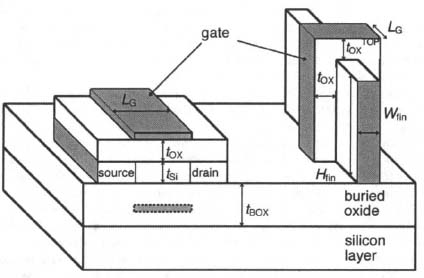
Figure 1. Three-dimensional sketch of the simulated SG SOI, DG SOI and fln-FET (not to scale). The grey-shadowed dashed line region represents the second gate for the DG SOI transistor.
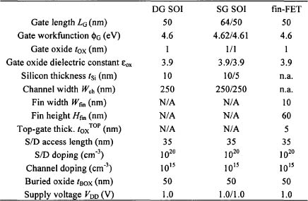
Table 1. Key parameters adopted in the comparison presented in Section 4. Third column reports two different SG SOI architectures, defined to have the same isothermal electrical characteristics as DG SOI and fin-FET.
As we are interested in the impact of self-heating, care has been taken in order to ensure the same IT electrical characteristics for all the devices, that is the same threshold voltage VT, the same transconductance and a good tolerance to the SCE (i.e. we have designed the structures in order to have drain-induced barrier lowering values lower than 100 mV/V).
A pure SiO2 gate dielectric with tOX = 1 nm has been chosen. In the fin-FET, the top gate features an oxide much thicker than the lateral ones (tOXΤΟΡ = 5 nm), so that the contribution to the drain current due to the top gate is negligible. The DG SOI and fin-FET transistors feature the same LG = 50 nm, as well as the same silicon thickness (tSi = Wfin = 10 nm).
The SGSOI architecture is strongly affected by SCE. In order to overcome this problem, two different solutions in designing the SG SOI transistor have been adopted: the first one (SG-1) features tSi = 10 nm but a slightly longer LG = 64 nm than the DG SOI and fin-FET; the second one (SG-2) features the same LG as DG SOI and fin-FET but a much thinner silicon body, tSi = 5 nm. While the fin-FETs’ fin width is set to 10 nm, the planar SOI devices feature a channel width Wch = 5LG, a realistic minimum width for planar devices.
Figure 2 shows the transfer and output characteristics, obtained from IT simulations. The devices feature almost the same IT currents per unit width, as required for a consistent comparison. Conversely, Figure 3 shows the transfer and output characteristics obtained from ET simulations. In these simulations, the gate and S/D contacts are taken as adiabatic, so the power generated in the active region can be dissipated only through the BOX. The SHE-related degradation of IDS strongly depends on the device structure: it is maximum for the DG SOI, less critical for the fin-FET, and minimum for SG-1. This trend is confirmed by Fig. 4, where the maximum temperature rise ΔTΜΑΧ ≡ (TMAX – 300 K), with TMAX being the maximum temperature reached inside the device, is plotted as a function of the dissipated power Ρ per unit width. The slope of each line can be interpreted as the thermal resistance RTH associated to the corresponding device; the table inset in the same figure reports RTH values for VGS = VDS = VDD. The DG SOI presents the highest thermal resistance, SG-1 the lowest one. The differences between SG SOI and the other two structures are related to the wider overlap area between the Si body and the underlying BOX, through which most of the heat flux occurs. This area is smaller in DG SOI and fin-FET (in particular, it is halved in DG SOI, with respect to SG SOI), and this degrades the heat dissipation. Furthermore, the larger SHE of SG-2 compared to SG-1 is due to the degradation of kSi occurring as tSi is scaled down from 10 nm in SG-1 to 5 nm in SG-2. The fin-FET presents lower SHE than DG SOI because Wfin is much lower than Wch, see Table 1. In this case, heat dissipation in the direction of device width is larger in the fin-FET than in the DG SOI. The relevance of this component increases as the device width decreases, as can be seen in Fig. 5: as Wch of the DG SOI is scaled down, the values of ION and TMAX depart from those obtained from the 2D DGSOI simulation (corresponding to infinite Wch), and approach the fin-FET values.
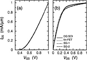
Figure 2. (a) Transfer characteristics at VDS = 1.0 V and (b) output characteristics at VGS = 1.0 V, calculated by 3D drift-diffusion isothermal simulations. The figure confirms that the different devices feature similar /( V) curves.
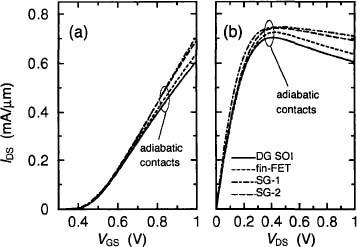
Figure 3. (a) Transfer characteristics at VDS = 1.0 V and (b) output characteristics at VGS = 1.0 V, calculated by 3D drift-diffusion electrothermal simulations. The gate and S/D contacts are treated as adiabatic and the heat flux can occur only through the buried oxide.
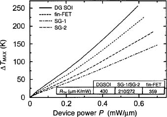
Figure 4. ΔTΜΑΧ = (TΜΑΧ − 300 K) vs. dissipated power per unit width P, for the four considered devices; the gate and S/D contacts are treated as adiabatic. As in Fig. 3, SG-1 presents the lowest temperature rise and equivalent thermal resistance RmH (i.e. RmH =ΔTΜΑΧ/P). The inset in the figure shows RmH values for VGS = VDS = VDD.
Figure 6 shows the transfer and output characteristics, obtained from ET simulations, when the S/D and gate contacts are treated as 300 K boundary conditions. In this case they act as cooling contacts, and they contribute to dissipating the heat generated in the active region. The differences between the devices in terms of drain current degradation become less evident compared to Fig. 3: most of the cooling occurs through the S/D contacts and the cross-sectional area of the S/D access regions become the most relevant parameter, leading to larger SHE in the SG-2 and DG SOI cases, compared to SG-1 and fin-FET. For the forthcoming technological nodes, the distance between the active region and the S/D contacts is expected to be scaled down; this trend could exploit the cooling occurring through the contacts and contribute to keep SHE under control.
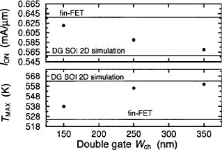
Figure 5. /ON at VGS = VDS = VDD (top) and TMAX (bottom) vs. DG SOI channel width Wch. The gate and S/D boundary conditions are assumed adiabatic, so the heat dissipation can occur only through the BOX. As Wch decreases, the values depart from the 2D DG SOI simulation case (Infinite Wch) and approach the fin-FET case.
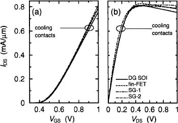
Figure 6. (a) Transfer characteristics at VDS = 1.0 V and (b) output characteristics at VGS = 1.0 V, calculated by 3D DD electrothermal simulations. The gate and S/D contacts are treated as 300 K isothermal boundary conditions.
6. Conclusions
We performed 3D fully-coupled electrothermal simulations of different SOI structures. Planar SG and DG as well as fin-FET transistors have been analyzed, in order to explore how self-heating effects impact the device performance of these different architectures. The results have been compared to reference isothermal electrical characteristics. Our simulations show that SHE detrimentally impacts the device performance and that it is structure-dependent. In particular, the thermal resistance associated with the S/D access regions, as well as the ratio between the surface available for the vertical heat dissipation through the buried oxide and the volume of the active region, largely differ from structure to structure.
References
1. R. Dennard, F. H. Gaensslen, V. L. Rideout, E. Bassous, and A. LeBlanc, “Design of ion-implanted MOSFETs with very small physical dimensions,” IEEE J. Solid-State Circ. 9, 256 (1974).
2. G. Baccarani, M. R. Wordeman, and R. Dennard, “Generalized scaling theory and its application to a 1/4 micrometer MOSFET design,” IEEE Trans. Electron Dev. 31, 452 (1984).
3. The International Technology Roadmap for Semiconductors, 2005 ed., is available at http://www.itrs.net
4. A. Asenov, A. R. Brown, J. H. Davies, S. Kaya, and G. Slavcheva, “Simulation of intrinsic parameter fluctuations in decananometer and nanometer-scale MOSFETs,” IEEE Trans. Electron Dev. 50, 1837 (2003).
5. E. J. Nowak, “Maintaining the benefits of CMOS scaling when scaling bogs down,” IBM J. Res. Develop. 46, 169 (2002).
6. V. De and S. Borkar, “Technology and design challenges for low power and high performance,” Proc. ISLPED (1999), pp. 163−8.
7. W. Haensch, E. J. Nowak, R. H. Dennard, et al., “Silicon CMOS devices beyond scaling,” IBM J. Res. Develop. 50, 339 (2006).
8. E. P. Gusev, V. Narayanan, and M. M. Frank, “Advanced high-κ dielectric stacks with poly-Si and metal gates: Recent progress and current challenges,” IBM J. Res. Develop. 50, 387 (2006).
9. H.-N. Lin, H.-W. Chen, C.-H. Ko, C.-H. Ge, H.-C. Lin, T.-Y. Huang, and W.-C. Lee, “Channel backscattering characteristics of strained PMOSFETs with embedded SiGe source/drain,” Tech. Digest IEDM (2005), pp. 141−1.
10. S. E. Thompson, M. Armstrong, C. Auth, et al., “A logic nanotechnology featuring strained-silicon,” IEEE Electron Dev. Lett. 25, 191 (2004).
11. R.-H. Yan, A. Ourmazd, and K. F. Lee, “Scaling the Si MOSFET: From bulk to SOI to bulk, “ IEEE Trans. Electron Dev. 39, 1704 (1992).
12. K. Suzuki, T. Tanaka, Y. Tosaka, H. Horie, and Y. Arimoto, “Scaling theory for double-gate SOI MOSFETs, “ IEEE Trans. Electron Dev. 40, 2326 (1993).
13. M. Asheghi, M. N. Touzelbaev, K. E. Goodson, Y. K. Leung, and S. S. Wong, “Temperature-dependent thermal conductivity of single-crystal silicon layers in SOI substrates,” J. Heat Transfer 120, 30 (1998).
14. Y. S. Ju and K. E. Goodson, “Phonon scattering in silicon films with thickness of order 100 nm,” Appl. Phys. Lett. 74, 3005 (1999).
15. W. Liu and M. Asheghi, “Thermal conductivity measurements of ultrathin single crystal silicon layers,” J. Heat Transfer 128, 75 (2006).
16. W. Liu, K. Etessam-Yazdani, R. Hussin, and M. Asheghi, “Modeling and data for thermal conductivity of ultrathin single-crystal SOI layers at high temperature,” IEEE Trans. Electron Dev. 53, 1868 (2006).
17. E. Pop, J. Rowlette, R. W. Dutton, and K. E. Goodson, “Joule heating under quasi-ballistic transport conditions in bulk and strained silicon devices,” Proc. SISPAD (2005), pp. 307−10.
18. S. Kumar, R. V. Joshi, C.-T. Chuang, K. Kim, J. Y. Murthy, K. T. Schonenberg, and E. J. Nowak, “Self-consistent and efficient electrothermal analysis for poly/metal gate fin-FETs,” Tech. Digest IEDM (2006), pp. 803−6.
19. G. K. Wachutka, “Rigorous thermodynamic treatment of heat generation and conduction in semiconductor device modeling,” IEEE Trans. Computer-Aided Design Integr. Circuits Syst. 9, 1141 (1990).
20. D. G. Cahill, W. K. Ford, K. E. Goodson, et al., “Nanoscale thermal transport,” J. Appl. Phys. 93, 793 (2003).
21. S. Sinha and Κ. E. Goodson, “Review: Multiscale thermal modeling in nanoelectronics,” Intern. J. Multiscale Comput. Eng. 3, 107 (2005).
22. S. Sinha, E. Pop, and K. E. Goodson, “A split-flux model for phonon transport near hotspots,” ASME Electronic Photonic Packaging 4, 75 (2004).
23. J. Rowlette, E. Pop, S. Sinha, M. Panzer, and K. Goodson, “Thermal simulation techniques for nanoscale transistors,” Proc. ICCAD (2005), pp. 225−8.
24. Sentaurus Synopsis, ver. X-2005.10.
25. C. Canali, G. Majni, R. Minder and G. Ottaviani, “Electron and hole drift velocity measurements in silicon and their empirical relation to electric field and temperature,” IEEE Trans. Electron Dev. 22, 1045 (1975).
26. J. D. Bude, “MOSFET modeling into the ballistic regime,” Proc. SISPAD (2000), pp. 23−6.
27. P. Palestri, D. Esseni, S. Eminente, C. Fiegna, E. Sangiorgi, and L. Selmi, “Understanding quasi-ballistic transport in nano-MOSFETs: Part I - scattering in the channel and in the drain,” IEEE Trans. Electron Dev. 52, 2727 (2005).
28. S. Eminente, D. Esseni, P. Paiestri, C. Fiegna, L. Selmi, and E. Sangiorgi, “Understanding quasi-ballistic transport in nano-MOSFETs: Part II -technology scaling along the ITRS,” IEEE Trans. Electron Dev. 52, 2736 (2005).
29. C. Fiegna, Y. Yang, E. Sangiorgi, and A. G. O’Neill, “Analysis of self-heating effects in ultrathin-body SOI MOSFETs by device simulation,” IEEE Trans. Electron Dev. 55, 223 (2008).
30. P. He, L. Liu, and Z. Li, “Measurement of thermal conductivity of buried oxides of silicon-on-insulator wafers fabricated by separation by implantation of oxygen technology,” Appl. Phys. Lett. 81, 1896 (2002).
31. M. Braccioli, G. Curatol, Y. Yang, E. Sangiorgi, and C. Fiegna, “Simulation of self-heating effects in different SOI MOS architectures,” Solid State Electronics 53, 445 (2009).